164 | P a g e
A REAL TIME IMPLEMENTATION OF SERIAL
COMMUNICATION BETWEEN GRAPHICAL USER
INTERFACE AND SIMULATION BOARD USING
ETHERNET
Juveria Fatima
1, Sharath Kumar
21
Digital Systems (M.E), ECE Department,
Muffakham JAH College of Engineering, Hyderabad, Telangana,, (India)
2
Computational Electronics (M.Tech),ECE Department,
Rajiv Gandhi University, Basara, Andhra Pradesh (India)
ABSTRACT
Virtex Series based FPGA is being used for establishing communication between different subsystems. To establish
the link, Ethernet is used. The objective of this work is to establish link between simulation board and Graphical
User Interface (GUI)[1]. The work can be divided into three steps. Step I, a Graphical User Interface (GUI) is
designed and developed based on LabVIEW Platform which enables the user to control the data. The selected data
is encoded in a predefined format and that data is sent to the simulation board using Ethernet serial link. Step I is
processed using PC. In step II, the hardware design is done, which includes the designing methods using XPS, EDK
software tools. In step III, the Software design is done, which includes the designing methods using SDK and the
decoding of coded data to identify the corresponding parameter data to generate the required output. This
generation of data is carried out by developing a code using Embedded C language. Step II is processed by using
Power processor. The three steps are finally integrated and the output can be validated on Microsoft Network
Monitor and TeraTerm serial tools.
Keywords- Ethernet, GUI, Microsoft Network Monitor, Power processor, XPS
I. INTRODUCTION
Virtex family provides most powerful features in the FPGA[2]. It contains distinct platforms. Each platform
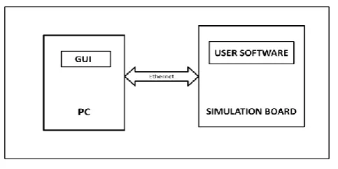
contains a different set of features. One of the functions of the Simulation board is to accept the data from
Graphical User Interface (GUI) which will be in frame format according to protocol, which is sent using
165 | P a g e
Fig 1.1 Connection between the GUI and simulation board
Fig 1.1 shows the connection between the GUI and simulation board. The Simulation board, after reception of data
will decode the data message, acknowledges the GUI, and sends the received data to the FPGA. FPGA is developed
on Embedded C programming language which will process the data. According to the received data, FPGA will
convert received data into the required output format and finally patches them to the respected IO pins. The main aim
of this paper is to establish a serial communication between simulation board and Graphical User Interface (GUI).
The paper is segregated into four activities which will be carried out in three steps. STEP1: A GUI has to be designed
and developed based on LabVIEW Platform [3] provides the user with selection of data and converts them into
frames according to the protocol and sends to the developed user software using Ethernet link. STEP2: Development
of Hardware using EDK. This can be done by using Xilinx Platform Studio and Embedded Development Kit [4] for
required simulator board. STEP3: Development of Software according to the requirement, which can be dumped into
the FPGA to function accordingly. GUI acts an Interface between the simulator board and user. It is developed in
such a way that the data is processed and output will be shown as desired.
Graphical user interface
The function of Graphical User Interface is to generate the appropriate selected data to user software as done by
the Simulator board. Every Selected data from GUI will be executed by the user software. Input of the GUI is
selection of data by user, which is to be processed further. The output is a frame, which is sent using Ethernet
link.
Fig. 2.1 Block diagram of Graphical User Interface
The above Fig.2.1 shows the block diagram of GUI, Link initialization process is implemented same as it
implemented in the development process of user software. If the link is ok, then GUI will let the user to select
166 | P a g e
Fig. 2.2 Graphical User Interface flow diagram
Fig.2.2 represents the Graphical User Interface flow diagram. Once the data is selected by user, then GUI sends
the information to the user software in a frame format using Ethernet link. The frame structure will be according
to the protocol. After data is provided by user at first it is encoded and then given to the framing block. Once
encoding is done, and then selected code and data count fields are added to the data field. Next checksum is
calculated by performing XOR operation performed in byte by byte process and next start of frame and end of
frame bytes are added, which completes the framing process. The framed data is sent to the Simulator board,
and waits for the acknowledgement. GUI gets acknowledgement ACK or no acknowledgement NACK. Design
and development process of GUI is done by using LabVIEW tool.
User software development
The selected data is input to this user software from GUI, and the output is generation of given parameter data
on external IO pins.
Fig.3.1 Block diagram of user software
The above Fig.3.1 shows block diagram of user software, initially it checks for Link initialization, if link is
established, board looks for Start of Frame (SOF). Assembly of frames starts only after reception of a SOF
character until End of Frame (EOF) is detected. After receiving the total frame error checking will be done by
167 | P a g e
received frame data bytes (byte by byte) except SOF and EOF. After Calculation of checksum, anAcknowledgement ACK or NACK will be sent to GUI in response to the received data. De-framing is done by
removing unnecessary bytes from frame and extracts data bytes. Actual data bytes are send to user peripheral for
further processing. Data received in user peripheral is stored and converted to the required format. The practical
implementation of this is done by using Xilinx XPS (Xilinx platform studio). After successful link establishment,
both entitiesenter into the Data Transfer phase. Then the two communication nodes can exchange messages vice
versa. Once the user software enters into data transfer phase, it waits till the start of frame to be received, which
triggers the user software into frame receiver mode. Once the user software enters into frame receiver mode it
keeps on receiving the bytes till the end of frame is received. All the received bytes of frame are store as byte
array in the order they receive. Once the frame is received successfully, user software checks whether frame is
error free or not. Error checking consists following two stages.
1. It calculates the check sum and compares it with the actual check sum field present in the frame.
2. It counts the number of actual data bytes in frame and compares with the data count field.
If the check sum doesn„t matches with actual check sum field then it generates a negative acknowledgement
frame and sends to the GUI and it doesn„t go for further processing and simply looks for the new start of frame.
Negative acknowledgement frame is generated according to the protocol. It contains the data of received frame
and byte in the data field which represents the error in the frame to the GUI. If the frame is error free, then
application software looks whether all the bytes are received or not. It does this by comparing total length of
frame with message length value +5. If any one or both the cases fail then a negative acknowledgement is sent to
the GUI. The Fig. 3.3 represents the frame structure. Once if these two stages are succeeded then positive
acknowledgement frame is sent to GUI which contains received data and positive acknowledgement byte. If the
received frame is error free then it is send to the de-framing block. De-framing is done in order to extract the
actual data field by removing overheads in the frame. Once the data bytes are extracted, then data is send to the
newly created IP which contains actual application work. The peripheral stores the data in a particular register
according to the received data and process it further and converts it into required output format specified by the
received data.
Implementation
Implementation of this is done by using XILINX XPS tool[2, 3, 6]. As user software has to be implemented in
FPGA, implementation process is divided into two stages. First stage is implementation of hardware and next
stage is software implementation.
168 | P a g e
The fig.4.1 represents the tool flow overview of XPS. The system design flow simply combines the standardhardware flow used to create FPGA bit streams and standard software flow used to create processor ELF files.
The first step is to create the ‗System Netlist using the Embedded Developers Kit and instantiate that Netlist
into the design„s HDL code. The hardware design is then synthesized, merged and implemented using the exact
same flow as used with any other ‗black box„ core. While it is common to include a portion of the yet created
software image inside the FPGA using block RAM, the ‗Compiled BIT file created during this phase of
development only contains the systems hardware description. The second step is to create the ‗Board Support
Package„ (BSP) using the Software Developers Kit (SDK) and include the required drivers in the system„s C
code. The code is then compiled and linked with the various functions available in the BSP as same with any
other processor system. Because the embedded system is built using the FPGA fabric, the BSP is customized for
the particular set of peripherals included in the ‗System Netlist„. Unlike an off shelf general purpose processor,
every BSP is potentially unique and as such SDK is tasked with customizing a generic set of drivers as required
to properly support the ‗arbitrary processor system. Once the final set of peripherals and bus structures have
been solidified, the software and hardware flows can be run independently. Even if part or the entire software
image is stored using on-chip block RAM, the software flow does not require running the hardware flow from
scratch, when making software changes. Only if a change is made to the instantiated ‗System Netlist does the
hardware need to be implemented again before the new software image which relies on the architectural change
can be loaded and run. If the software image is completely stored externally, configuring the FPGA and loading
the external storage device are performed in exactly the same way as a typical two chip solution. If part or all of
the software image is stored using onchip block RAM and as such is embedded within the FPGA„s bit stream,
an additional step is required before the FPGA can be configured. EDK provides a tool called Data2MEM
which merges the appropriate sections of the ‗Compiled ELF„ file with the ‗Compiled BIT„ file. The resulting
BIT file is created typically created in a few seconds and can then be used to configure the FPGA. When the
entire software image is stored within the FPGA, only the BIT file is needed to configure the system and load
the software image. If only portion of the software image, such as the bootstrap, is stored within the FPGA, then
Data2MEM is run to create a combined BIT file and the system is once again configured/loaded as any two chip
solution using the unmerged ELF sections and the combined BIT file. Debugging the software running on the
system is performed in the same manner as would be on any general purpose processor.
Hardware Implementation
Hardware Implementation can be done as follows. First Invoke the XPS, create a new project and select the
Base System Builder Wizard. In the Base System Wizard, Create New XPS Project Using BSB Wizard window,
browse to a directory in which to write the project file (system.xmp), choose I would like to create a new design,
select Board window, select the board which suits. Next choose I would like to create a system. In the Board
Architecture field, select FPGA details. In the Base System Builder wizard, in Processor window, verify that the
PowerPC Processor is selected. Next Configure PowerPC Processor window make the selections as per your
requirements. Under Processor Configuration, for Debug Interface, accept FPGA JTAG as the Debug interface.
Next for Cache setup, uncheck Enable. Confirm that Enable Floating point unit (FPU) is unchecked. Next in the
Base System Builder - Configure I/O Interfaces window, make the selections as given below Check
RS232_Uart_1 then select XPS UARTLITE in the Peripheral field. Set The Baud Rate to 9600, the Data bits to
169 | P a g e
Hard_Ethernet_MAC. This will enable a tri mode Ethernet peripheral. Check Use Interrupt. Add InternalPeripherals (1 of 1) window, make the selections as below: For XPS BRAM IF CNTLR, select Memory of your
requirement. Next In the Base System Builder - Software Setup window, make the selections as below. In the
Boot Memory field, select xps_bram_if_cntrl_1. Under Sample Application Selection, check Memory Test
(default) and check Peripheral self test (default). In the Base System Builder - Configure Memory Test
Application window, make the selections as: In the Instruction, Data and Stack/Heap fields, select
xps_bram_if_cntlr_1.b In the Interrupt Vector field, select DDR_SDRAM (default). In the Base System Builder
- Configure Peripheral Test Application window, make the selections as below. In the Instruction, Data
Stack/Heap, and Interrupt Vector fields, select DDR_SDRAM. In the Base System Builder – System Created
window, where the selections which have been made are summarized, click Generate to generate the system. In
the Base System Builder - Finish window, check Save Settings File click Finish.
Software implementation
Software implementation can be done as follows. Select Software menu, go to Software platform settings to
select the software settings for the embedded system. In Software platform settings check Xilkernel, check lwip
and Xilmfs. In OS& Libraries settings configure the Xilkernel libraries according to requirements. Next in
driver window default drivers are configured. Select OK. Again select Software menu, go to Generate Libraries
and BSPs to generate libraries and board support packages. This will generate .MSS file. In Application area
select Add application project option and type the name of the application in the Project Name area and click
OK. A new application is created. In the created application add source files and header files which are used for
implementing the application. After writing the user software, build the application using Software Build all
User Applications for checking the errors and debugging the developed application. After completing the above
procedure .elf file for the application is generated it is used to download it onto the FPGA. Select Debug
→XMD Debug options select connection type to Hardware, JTAG Cable type Auto, check Auto discover JTAG
chain definition and click OK. Download bit stream to FPGA using JTAG using Device Configuration→
Download Bit stream to the FPGA. Here sytem.bit file and .elf file are merged in order generate download.bit
file and configures the FPGA through JTAG. When .elf file is not included in download.bit file then Select
Debug > Launch XMD from the XPS GUI to debug the user software. After launching XMD debugger
download .elf file of the application using the command download <application name>/executable.elf. Run the
application using the command run. Use stop command to stop the processor. The software part of the design is
configured using the SDK tool. In order to configure the software platform, the entire hardware design is
launched and exported to the SDK environment. In SDK, the required operating System is selected along with
the Light Weight Internet Protocol (lwIP). Now, to meet our application requirement, a C- program is written
wherein the server works on data and listens for the input at the specified port and simply echoes back whatever
data is sent to that port. In our design, the IP address 192.168.1.10 is binded with our board‟ s MAC address.
Also our design is configured such that it will be listening for the input at the port 7. After the data is echoed
back from the board to the PC, another embedded application software program is written in order to send the
commands initialized from the SCD to the Target Board. The output is finally verified using the GPIO pins and
170 | P a g e
Ethernet
Ethernet has been a relatively inexpensive, reasonably fast, and very popular LAN technology for several
decades. Two individuals at Xerox PARC -- Bob Metcalfe and D.R. Boggs -- developed Ethernet beginning in
1972 and specifications based on this work appeared in IEEE 802.3 in 1980. Ethernet has since become the most
popular and most widely deployed network technology in the world. The Ethernet standard has grown to
encompass new technologies as computer networking has matured. Specified in a standard, IEEE 802.3, an
Ethernet LAN typically uses coaxial cable or special grades of twisted pair wires. Ethernet is also used in
wireless LANs. Ethernet uses the CSMA/CD access method to handle simultaneous demands. The most
commonly installed Ethernet systems are called 10BASE-T and provide transmission speeds up to 10 Mbps.
Devices are connected to the cable and compete for access using a Carrier Sense Multiple Access with Collision
Detection (CSMA/CD) protocol. Fast Ethernet or 100BASE-T provides transmission speeds up to 100 megabits
per second and is typically used for LAN backbone systems, supporting workstations with 10BASE-T cards.
Gigabit Ethernet provides an even higher level of backbone support at 1000 megabits per second (1 gigabit or 1
billion bits per second). 10-Gigabit Ethernet provides up to 10 billion bits per second.
Results
Fig.9.1: Establishing Connection operation Fig.9.2: Wireshark Output
171 | P a g e
Fig.9.3 Pinging Operation
CONCLUSION
Serial communication through Ethernet link has been successfully established between Graphical User Interface
and Simulator board. Subsequently selected data have been communicated between the Graphical User Interface
and Simulator board. The future scope of this work can be enhanced by suing wireless communication.
REFERENCES
[1] M. Srilatha, CH. Tejasree, SV. Kishore “A Real Time Implementation of Serial Communication between
Graphical User Interface and Simulator Board Using RS-232” International Journal of Engineering Trends and
Technology (IJETT) – Volume 4 Issue 8-August 2013
[2]Clive ―MAX‖ Maxfield, ―the design warrior‟s guide to FPGAs‖,2004.
[3]LabVIEW software tool- LabVIEW
[4]Xilinx software Help tool – Xilinx
[5]Xilinx Website -www.xilinx.com
[6]www.xilinx.com/support/documentation/dt_edk_edk10-1.htm.
[7]Embedded System Tools -Reference Manual - Xilinx
[8]Andrew S. Tanenbaum, “Computer Networks”, Third Edition, Prentice Hall 1996.
[9]Ethernet: The Definitive Guide by Charles E. Spurgeon.
[10]IEEE Std 802.3-2002 Standard for Information Technology, IEEE Standards Association.