Transient Frequency Analysis and Kink Effect
Reduction of SOI MOSFET using Silvaco
TCAD Simulator
Shakti Verma
Department of Electronics and Communication Engineering
SISTech, Bhopal, M.P., India
Mohd Abdullah
Department of Electronics and Communication Engineering
SISTech, Bhopal, M.P., India
Nitin Muchhal
Department of Electronics and Communication Engineering SISTech, Bhopal, M.P., India
Abstract - With the emergence of mobile computing, automation and communication, low power device design and implementation have got a significant role to go through VLSI design. Conventional silicon technology has suffered from the fundamental physical limitations in the sub-micron or nanometer region. These requirements have led to development of alternative technology. Silicon-On-Insulator (SOI) technology is one such substitute which can offer the performance as may be expected from next generation Si technology. In spite of benefits of SOI devices several limitations like “Kink” in the output voltage-current characteristics, self-heating etc., which are absent in bulk devices, limit the device performance. This paper provides a complete investigation of the kink effect in SOI MOSFET and proposes a method for eliminating kink effect. To eliminate the kink effect SELBOX method has been considered. In this method, back oxide for the device is introduced at selected regions underneath the source and drain. Selective back oxide structure with different gap lengths and thicknesses has been studied. Results obtained through numerical simulations indicate that the proposed structure can significantly reduce the kink while still maintaining major advantages offered by conventional SOI structure.
Keywords – BTC, Compression, quantization, algorithm, image retrieval, multimedia.
I.INTRODUCTION
With the emergence of mobile computing, automation and communication, low power device design and implementation have got a significant role to go through VLSI design. Conventional silicon technology has suffered from the fundamental physical limitations in the sub-micron or nanometer region. These requirements have led to development of alternative technology. Silicon-On-Insulator (SOI) technology is one such substitute which can offer the performance as may be expected from next generation Si technology. In spite of benefits of SOI devices several limitations like “Kink” in the output voltage-current characteristics, self-heating etc., which are absent in bulk devices, limit the device performance.
This paper provides a complete investigation of the kink effect in SOI MOSFET and proposes a method for eliminating kink effect. To eliminate the kink effect SELBOX method has been considered. In this method, back oxide for the device is introduced at selected regions underneath the source and drain. Selective back oxide structure with different gap lengths and thicknesses has been studied. Results obtained through numerical simulations indicate that the proposed structure can significantly reduce the kink while still maintaining major advantages offered by conventional SOI structure.
II.PROPOSED METHODLOGY
Following TCAD programs are used for the modeling and simulations of the Silicon-on-insulator device [13]: The first one is Deck build, it runs the code, and provided the interface for changing and altering the code. Second one is TONYPLOT, which is used for graphing the data extracted from the simulation.
Third one is Atlas, which is use to actually simulate the SOI device and to extract the data.
ATLAS is a two and three dimensional physical based device simulator. It predicts the electrical behavior of specified semiconductor structures and provides insight into the internal physical mechanisms associated with device operation.
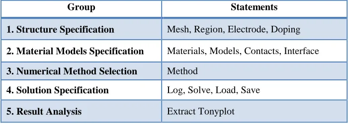
The order in which statements occur in an ATLAS input file is important. There are five groups of statements that must occur in the correct order. Failure to do so usually causes an error message to appear, which could lead to incorrect operation or termination of the program. For example, if the material parameters or models are set in the wrong order, then they may not be used in the calculations.
The order of statements within the mesh definition, structural definition, and solution groups is also important. Failure to place these statements in proper order may also cause incorrect operation or termination of the program.
Table - 1 ATLAS Design Flow
Group Statements
1. Structure Specification Mesh, Region, Electrode, Doping
2. Material Models Specification Materials, Models, Contacts, Interface
3. Numerical Method Selection Method
4. Solution Specification Log, Solve, Load, Save
5. Result Analysis Extract Tonyplot
2.1 Structure Specification
To define a device through the ATLAS command language, we must first define a mesh. This mesh or grid covers the physical simulation domain. The mesh is defined by a series of horizontal and vertical lines and the spacing between them. Then, regions within this mesh are allocated to different materials as required to construct the device. For example, the specification of a MOS device requires the specification of silicon and silicon dioxide regions. After the regions are defined, the location of electrodes is specified. The final step is to specify the doping in each region. 2.1.1 Specifying the Initial Mesh
The mesh is a series of horizontal and vertical lines that form a grid, or mesh, which defines the area where the device will be built. Each spot where the lines cross is a point where the program will analyze the structure, so the lines should cross frequently in areas of interest, and less frequently in areas where the structure is less active.
For MOSFET, SOI & SELBOX structure same grid has been specified:
X = 0 to 3 micron with proper spacing &
Y = -0.017 to 0.7 micron, where at -0.017 micron gate has been structured.
2.1.2 Specifying Regions
Once the mesh is specified, every part of it must be assigned a material type. It is done by specifying regions.
2.1.3 Specifying Electrodes
Once we have specified the regions and materials, define at least one electrode that contacts a semiconductor material.
Table - 3 Electrode definition
Electrode Gate Source Drain
Electrode 1 x= 1 to 2 micron location &
y= -0.017 to -0.017 micron --- ---
Electrode 2 --- x= 0 to 0.5 micron location &
y= 0 to 0 micron ---
Electrode 3 --- --- x= 2.5 to 3 micron location &
y= 0 to 0 micron
2.1.4 Specifying Doping
We can specify analytical doping distributions, or have ATLAS read in profiles that come from either process simulation or experiment.
Doping Concentration
P-type doping of uniform concentration = 1e17 n-type doping concentration = 1e20
set interface charge separately on front and back oxide interfaces Front oxide interface charge = 3e10
Back oxide interface charge = 1e11
2.2 Material Models Specification
2.2.1 Defining Material Parameters
Once the mesh, geometry, and doping profiles are defined, we can modify the characteristics of electrodes.
2.2.2 Specifying Physical Models
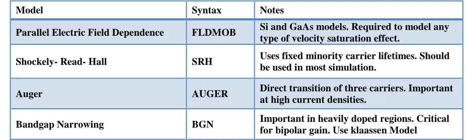
Physical models are specified using the MODELS and IMPACT statements. Parameters for these models appear on many statements including: MODELS, IMPACT, MOBILITY, and MATERIAL. The physical models can be grouped into five classes: mobility, recombination, carrier statistics, impact ionization, and tunneling. The following models are used during simulation.
Models used in this paper
recombination model = auger
shockley-read-hall recombination model with fixed carrier lifetimes = srh concentration dependant mobility model = conmob
Impact ionization model = Selberherr model DEVICE/
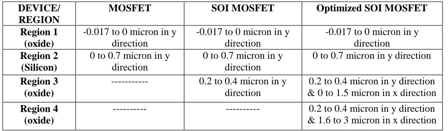
REGION
MOSFET SOI MOSFET Optimized SOI MOSFET
Region 1 (oxide)
-0.017 to 0 micron in y direction
-0.017 to 0 micron in y direction
-0.017 to 0 micron in y direction Region 2
(Silicon)
0 to 0.7 micron in y direction
0 to 0.7 micron in y direction
0 to 0.7 micron in y direction
Region 3 (oxide)
--- 0.2 to 0.4 micron in y direction
0.2 to 0.4 micron in y direction & 0 to 1.5 micron in x direction Region 4
(oxide)
--- --- 0.2 to 0.4 micron in y direction
parallel field mobility = fldmob Band gap narrowing = bgn
Table - 4 Model Used in Simulation
2.3 Choosing Numerical Methods
Several different numerical methods can be used for calculating the solutions to semiconductor device problems. Different combinations of models will require ATLAS to solve up to six equations. For each of the model types there are basically three types of solution techniques:
(a) Decoupled (GUMMEL): The GUMMEL method will solve for each unknown in turn keeping the other variables constant, repeating the process until a stable solution is achieved.
(b) Fully coupled (NEWTON): The NEWTON method solves the total system of unknowns together and (c) BLOCK: The BLOCK methods will solve some equations fully coupled, while others are de-coupled. 2.4 Solution specification
2.4.1 Obtaining solution
Obtaining solutions is rather analogous to setting up parametric test equipment for device tests. We define the voltages on each of the electrodes in the device. ATLAS then calculates the current through each electrode. ATLAS also calculates internal quantities, such as carrier concentrations and electric fields throughout the device. This is information that is difficult or impossible to measure.
In all simulations, the device starts with zero bias on all electrodes. Solutions are obtained by stepping the biases on electrodes from this initial equilibrium condition. ATLAS due to the initial guess strategy, voltage step sizes are limited.
Transient Solutions
Transient solutions can be obtained for piecewise-linear, exponential, and sinusoidal bias functions. Transient solutions are used when a time dependent test or response is required.
2.5 Interpreting the Results
Run-time output is provided at the bottom of the DeckBuild Window. Errors occurring in the run-time output will be displayed in this window. Note that not all errors will be fatal. This may cause a statement to be ignored, leading to unexpected results.
Model Syntax Notes
Parallel Electric Field Dependence FLDMOB Si and GaAs models. Required to model any type of velocity saturation effect.
Shockely- Read- Hall SRH Uses fixed minority carrier lifetimes. Should
be used in most simulation.
Auger AUGER Direct transition of three carriers. Important
at high current densities.
Bandgap Narrowing BGN Important in heavily doped regions. Critical
III. MODELING & SIMULATION OF THE PROPOSED MOS STRUCTURE
In this paper MOSFET, SOI MOSFET and Optimized SOI MOSFET structure has been fabricated according to the methodology proposed in earlier chapter. Transient analysis has been implemented and frequency analysis has been carried out.
3.1 Modeling and Simulation of MOSFET Structure
The traditional metal–oxide–semiconductor (MOS) structure is obtained by growing a layer of silicon dioxide (SiO2) on top of a silicon substrate and depositing a layer of metal or polycrystalline silicon (the latter is commonly used). As the silicon dioxide is a dielectric material, its structure is equivalent to a planar capacitor, with one of the electrodes replaced by a semiconductor. When a voltage is applied across a MOS structure, it modifies the distribution of charges in the semiconductor.
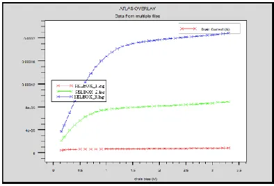
At the end of the simulation extract is used to measure the peak current and the saturation slope. From the shape of the ID-VD curves the saturation slope is clearly the minimum value of the gradient along the curve. ID-VD characteristic curve is overlaid in Tonyplot.
The MOSFET is simulated at ramp gate voltage 1v, 2v & 3v and ID – VD characteristic graph has been plotted.
3.2 Simulation Analysis of SOI structure
When a layer of silicon dioxide is introduced in the silicon in MOSFET structure, the physical limitation of MOSFET such as reduction in carrier mobility due to impurities, increasing gate tunneling effect as the gate oxide thickness decreases and increasing p-n junction leakage current as the junctions become more and more shallow has been eliminated.
SOI technology offers significant advantages in design, fabrication and performance for many semiconductor circuits such as excellent isolation, improved latch up free operation, radiation hardness, reduced leakage current, reduced short channel effects and improved switching speeds due to reduction in the drain-body capacitance. The
reduction in the parasitic capacitances leads to improved switching speed and superior performance.
3.3 Simulation analysis Optimized SOI MOSFET structure
To reduce the kink effect it is needed to be optimize the SOI structure. For the optimization we introduced different gap thickness between the oxide layer. When we provide the gap between the oxide, the impact ionization arised due to BOX is reduced because of the bypassing the carriers in the substrate region.
In this paper SOI structure has been modified for the gap length of 0.001micron, 0.01 micron, 0.1 micron, 0.2 micron & 1 micron between the BOX layer.
Now the SELBOX structure has been optimized to get the gap length at which kink effect eliminate while
preserving the characteristics of SOI. For the optimization the SELBOX structure is given the variable gap length of 0.01 micron , 0.1 micron, 0.2 micron & 1 micron. The simulated result shows the critical gap length at which kink is eliminated is 0.1 micron. The characteristic graph has been discussed in the next chapter.
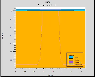
The obtained optimized structures are shown below with varying gap length.
Figure 5 : SELBOX structure with gap length 0.001micron Figure 6 : SELBOX structure I
D-VDS graph for 0.001 micron gap length At V = 1v, 2v, 3v
Figure 7: SELBOX structure with gap length 0.01micron
3.4 Frequency Response Analysis For MOSFET
The transition frequency can be calculated by
(1)
Where,
At saturation: ,
Putting these values we can get the value for
figure 9: selbox structure with gap length 0.1micron Figure 10: SELBOX structure ID-VDS graph for 0.1 micron gap length At VG = 1v, 2v, 3v
Figure 11: SELBOX structure with gap length 0.2 micron Figure 12: SELBOX structure ID-VDS graph for 0.2 micron gap length At VG = 1v, 2v, 3v
We have,
(2) Where
Putting the value of and
We get
We have and m
By putting these values we have
We have
(3)
(4)
We have and
Now by putting the value of all capacitance and Transconductance we can get the value of transition frequency for MOSFET
For SOI MOSFET
The presence of the buried oxide in SOI devices minimizes the capacitance . The capacitance between gate and substrate seen in case of bulk devices will have two capacitor components connected in series for SOI devices. Here it will be a series combination of capacitance between gate and the body region and the which is the capacitance between body of the SOI device and substrate at the bottom end where buried oxide is the dielectric. With the introduction of , the capacitance will be reduced to an extremely low value and the transition frequency for SOI devices from equation 3.1 is reduced to
(5)
Now by putting the value of all capacitance and Transconductance we can get the value of transition frequency for SOI MOSFET is
For Optimized SOI MOSFET (SELBOX structure)
For SELBOX structure the device is obtained by modifying the layout of the buried oxide. The buried oxide does not cover the entire area below the source and drain as in the case of SOI devices. For SELBOX structure the gate to substrate capacitance depends on the gap of the buried oxide. Consequently in the SELBOX structure the capacitance will not be negligibly small as compared to the SOI devices but will assume a value much less than that for bulk devices. Consequently the transition frequency for SELBOX structures is expected to be higher than that for simple bulk devices.
(6)
(7)
For gap length of 0.1 micron
Here, W= 2.5 and
Putting all these values we can get the value of
For gap length of 0.2 micron
Here, W= 2.5 and
Putting the value of capacitance in equation 3.6 We get
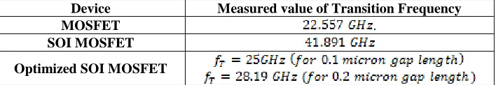
Device Measured value of Transition Frequency
MOSFET .
SOI MOSFET
Optimized SOI MOSFET
Table 5: Transition frequency of simulated device
IV.CONCLUSION
MOSFET, SOI MOSFET & SELBOX structure has been implemented using the Silvaco TCAD tools. In order to avoid the physical limitations of traditional methods, SOI technology came into existence. SOI technology offers significant advantages in design, fabrication and performance for many semiconductor circuits such as excellent isolation, improved latch up free operation, radiation hardness, reduced leakage current, reduced short channel effects and improved switching speeds due to reduction in the drain-body capacitance. In spite of these SOI suffers with several limitations like “Kink” in the output current-voltage characteristics, self-heating etc. which are not present in bulk devices.
In order to reduce the kink effect SELBOX structure has been proposed. By optimization of the SELBOX structure kink can be eliminated effectively.
From the optimization of SOI MOSFET structure it has been observed that at 0.1 micron the device eliminates the kink while preserving the basic merits of SOI structure. Below than 0.1 micron of gap length between the oxides the kink is partially reduced at low ramp voltage. Hence it should not be used in specific application otherwise due to the kink the device will suffer with self-heating and it can be the reason of damage of the device.
At 0.2 micron the device gives better response than at 0.1 micron gap length in terms of transition frequency. SELBOX structure with higher gap length like 1 micron will behave like MOSFET. There is no kink but the device will suffer with the same limitation as of MOSFET. The device will not be more radiation hardness.
REFERENCES
[1] A. Mercha, J. M. Rafí, E. Simoen, E. Augendre, and C. Claeys ““Linear Kink Effect” Induced by Electron Valence Band Tunneling in Ultrathin Gate Oxide Bulk and SOI MOSFETs” IEEE transactions on electron devices, vol. 50, NO. 7, july 2003
[2] B. G. Vasallo, J. Mateos, D. Pardo and T. Gonzalez “ Monte Carlo study of kink effect in short-channel InAlAs/ InGaAs high electron mobility transistors” Journal Of Applied Physics, Volume 94, Number 6, 2003
[3] Bennamane Kamal, Benfdila Arezki, Achour Hakim and Lakhlef Ahcene “On Silicon on Insulator Technology and Devices”, African Physical Review 2 Special Issue (Microelectronics): 0003, 2008.
[4] Rahul Kr. Singh, Amit Saxena, Mayur Rastogi “Silicon On Insulator Technology Review” International Journal of Engineering Sciences &
Emerging Technologies, Volume 1, Issue 1, May 2011.
[5] Sapna & Bijender Mehandia “Study of Electrical Characteristics of SOI MOSFET Using Silvaco TCAD Simulator” , Current Trends in Technology and Sciences Volume : 1, Issue : 1 ,July-2012J. Eggers, J. Su and B. Girod," Robustness of a Blind Image Watermarking Scheme", Proc. IEEE Int. Conf. on Image Proc., Vancouver, 2000.
[6] H. Morris, E. Cumberbatch, V. Tyree, H. Abebe “Analytical Results for the I-V Characteristics of a Fully Depleted SOI-MOSFET” research work submitted for the publish
[8] Benjamin iniguez, jean pierre raskin, pascal simon, denis flandre & jaume segura “A review of leakage current in SOI CMOS ICs: impact on parametric testing techniques”, Solid-State Electronics 47 2003.
[9] Ling Wang, Tor A. Fjeldly, Benjamin Iniguez, Holly C. Slade & Michael Shur “Self-Heating and Kink Effects in a-Si: H Thin Film Transistors”, IEEE Transactions On Electron Devices, VOL. 47, NO. 2, February 2000.P.
[10] Sanjoy Deb, C. J. Clement Singh, Subir Kumar Sarkar, N Basanta Singh & P C Pradhan, “Design and Performance Comparison of SOI and Conventional MOSFET based CMOS Inverter”, published by International Journal of Computer Applications, 2011
[11] Dewill Chung, Byong-Deok Choi, Sang-Gyu Park, “A New Model for Kink-Effect in Poly-Silicon Thin-Film Transistors”, Proc. of ASID, 8-12 Oct, 2006
[12] M. Youssef Hammad and Dieter K. Schroder, “Analytical Modeling of the Partially-Depleted SOI MOSFET”, IEEE Transactions On Electron Devices, Vol. 48, No. 2, February 2001.