Abstract— The 430MHz high efficiency RF transmitter for wireless body area network in medical application is presented in this paper. Transmitter architecture with high energy efficiencies is proposed to achieve high data rate with low power consumption. In conventional transmitters, the oscillator and power amplifier are turned off when the transmitter sends 0 data. The required time for ON/OFF LC-oscillators is higher than the other blocks of transmitter. In the proposed transmitter low power ring oscillator is proposed. All blocks of TX are turned off when “0” data is sent. The transmitter consumes 2.3 mW with 60 Mbps data rate and energy consumption 42 pJ/(bit×mW) per transmitted bit with -0.37 dBm output power. The proposed transmitter designed in 0.18µmCMOS technology.
Index Term— Wireless Body Area Network, Transmitter, Power Amplifier, Output Power, On-Off keying, Low Power, Ring oscillator
.
I. INTRODUCTION
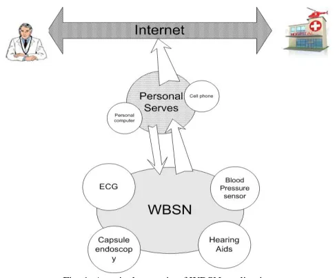
Wireless body sensor network provides wireless connectivity among sensors which are used for exhibition signals vital of body and personal serves. Vital signal monitoring, diagnose assistant, and the drug delivery are medical application of WBAN [1, 4]. Personal computer, cell phone, wireless local array network (WLAN) and internet network are personal serves used to connect with medical center and WBAN. Fig. 1 illustrates a typical scenario of WBAN application.
M. Yousefi is with the Faculty of Electrical and Computer Engineering, University of Tabriz, Tabriz, IRAN (phone: +989143067540; e-mail:
m.yousefi@ tabrizu.ac.ir).
Z. D. Koozehkanani is with Faculty of Electrical and Computer Engineering, University of Tabriz, Tabriz, IRAN (e-mail: zdaie@
tabrizu.ac.ir).
J. Sobhi is with Faculty of Electrical and Computer Engineering, University of Tabriz, Tabriz, IRAN (e-mail: sobhi12@ yahoo.com). N. Nasirzadeh Azizkandi is with the Faculty of Electrical and Computer Engineering, University of Tabriz, Tabriz, IRAN (e-mail: nnasirzadeh@
tabrizu.ac.ir).
Fig. 1. A typical scenario of WBSN application.
In typical WBAN applications, the distance between node and gateway node is less than 3m, and the output power for transmitter (TX) is less than 1mw. Sensor node is composed of sensing section, ADC, digital processor and transceiver. Sensor node must be small to limit the required source energy, while the transceiver consumes extra energy. As a result, the design of an RF transceiver is challenge for the WBSN sensor node. In most reported papers, figure of merit for transmitter is that how much energy is consumed for sending one bit by assuming that error did not occur in data transmission. Conventional FOM does not take the transmit power into account. Transmitters that have a high output power normally consume more dc power, which is a disadvantage. Through this work, an alternative FOM is used, denoted FOMTX, which normalizes the energy efficiency (FOM) to the output power, Po. That is,
/
TX o
FOM FOM P (1)
( ) / ( ( ) ( ))
TX DC o
FOM P mW DR Mbps P mW (2)
FOMTX has been used as a better FOM to compare different transmitters [3]-[4]. High data rate wireless connection is required for applications like capsule endoscopy or multichannel biosensor recording. In order to maximize the life time, data rate must be kept high while dc power is kept low. ON/OFF keying (OOK) and frequency shift keying (FSK) are dominant modulation methods in the RF transceiver of the sensor node.
A 430 MHz Fully Integrated High Efficiency
OOK Transmitter for Wireless Biomedical
Application
Where, PDC is transmitter's power consumption. In order to maximize the lifetime, data rate and dc power must be respectively high and low. High data rate wireless is required for applications like capsule endoscopy or multichannel biosensor recording. OOK and frequency shift keying (FSK) are the most common modulation schemes in the RF transceiver sensor node.
Transmitter architecture with high energy efficiencies is proposed to achieve high data rate with low power consumption. This paper is organized as follows. Section 2 describes the basic operation of the transmitter architecture used. Results are presented in Section 3. Finally, the conclusions are presented in Section 4.
II. TRANSMITTER STRUCTURE
The block diagram of the proposed transmitter (TX) is shown in Fig. 2. In this design, OOK modulation scheme is utilized, in which binary “1” is represented by a pulse and binary “0” by no pulse transmission. The TX adopts simple circuitry structure to save power. It is composed of two major building blocks: the oscillator and the PA. The OOK TX can be easily realized by turning on or off the PA and oscillator according to message data. However, all of components of the transmitter must be switched on and off with data rate frequency. The required time of ON/OFF duration of all the blocks determines the maximum data rate frequency. The required time for ON/OFF duration of oscillator is higher than the other blocks of TX.
PA Modulator
Message Data
Fig. 2. Block diagram of the transmitter
2-stage
1-stage 3-stage 4-stage
5stage 15-stage
15-Inverter Stage
X X X
X X
X
Vdd1
to PA
Fig. 3. The schematic of Ring oscillator with 15-Inverter stages
A. Digitalyl Controlled Oscillator
transmitter sends “0” data. The digitally controlled oscillator (DCO) is designed with the simplest type of ring oscillator, a 15-stage CMOS ring using standard library inverters. Other oscillators like LC oscillator is most used in transmitters but turning oscillators on or off is time consuming for start up so the data rate of TX is limited by rise and fall time of the oscillator. Also the LC oscillator requires large area for on-chip integration.
As reported in [5-6], the main disadvantage of the ring oscillator is its poor phase noise. But by employing large number of inverter stages, the phase noise of the oscillator can be improved. Increasing the number of stages increases the power consumption. There is a trade-off between the number of stages, power consumption and the frequency of the ring. In this proposed design, the oscillator is resonating at 430 MHz frequency with 1 mW dc power using 15 inverter stages. As seen in Fig. 4, frequency tuning of the oscillator is accomplished through calibration of the power supply of only 1 stage of 15 inverter stages. The circuitry of frequency tuning is shown in Fig. 4. It consists of the digital signals that are adopted to control the transistors for tuning the desired frequency. As seen in Fig. 4, the four transistors M0...M3 are
fine tuning and the M4...M7 transistors are for coarse tuning.
Simulation results show that the tuning range is about 0.428-0.438 MHz with a 100 kHz/LSB. The C0...C7 digital signals are
adopted to control the M0…M7 transistors. The oscillator sinks
about 1 mA average current from 1 volt power supply. The designed oscillator has -109 dBc/Hz (1MHz offset) frequency phase noise that is sufficient for OOK modulation. Power Amplifier
Reported topologies for WSN applications are invariably non-linear to achieve the best efficiency. Tuned circuits are employed in the output matching circuitry to block the non-linear products at the harmonic frequencies. Switched power amplifier like inverter with or without a current source as reported in [7][8], exhibits good efficiency since the conduction angle is very low. Also termed as push-pull topology, it maximizes gm/ID as the effective gm is doubled, as
it is the sum of PMOS and NMOS reusing the current.
C0 C1 C2 C3 C4 C5 C6 C7
Vdd1 Vdd
M0 M1 M2 M3 M4 M5 M6 M7
M8 M9
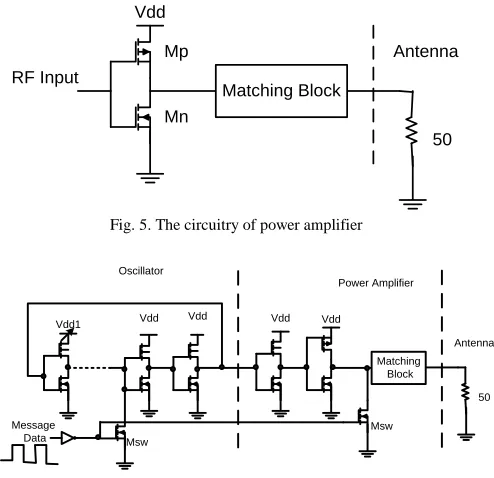
OOK modulation it suffers from poor isolation from output to input. Variations in the load impedance due to component variations, affects the input impedance, input swing, gain, dynamic current consumption and the frequency of the oscillator due to pulling. Poor isolation also leads to injection locking of the oscillator to the frequency of the signal at antenna port. Because an inverter driver has been used between the oscillator and PA, isolation will be improved. Thus we have designed this structure as shown in Fig. 5. In this PA, the matching block is integrated on the chip.
B. Modulator
The circuit diagram of the transmitter is shown in Fig. 6 Two transistors (Msw) are used to modulate carrier signal with
message data. For modulation of data with carrier, Msw
transistors are used to turn off oscillator and PA. When the transmitter sends "0" message data, Msw transistor turns on and
Msw transistor turns off when transmitter sends "1". In the
proposed design, data rate of the transmitter is determined by rise and fall time of PA. The results show that rise time and fall time of transmitter are better than other techniques.
C. Circuit design
The prototype of the transmitter was designed in the 0.18 µm CMOS process. The schematic of transmitter is shown in Fig. 5. In this design, data rate is limited by startup time of the power amplifier but not oscillator. Also, the comparison Table II shows that FOM for proposed circuit of proposed transmitter is better than other techniques. In the overall circuit the channel length of all transistors is 0.18 μm. The other characteristics of proposed TX are shown in Table I.
III. RESULTS
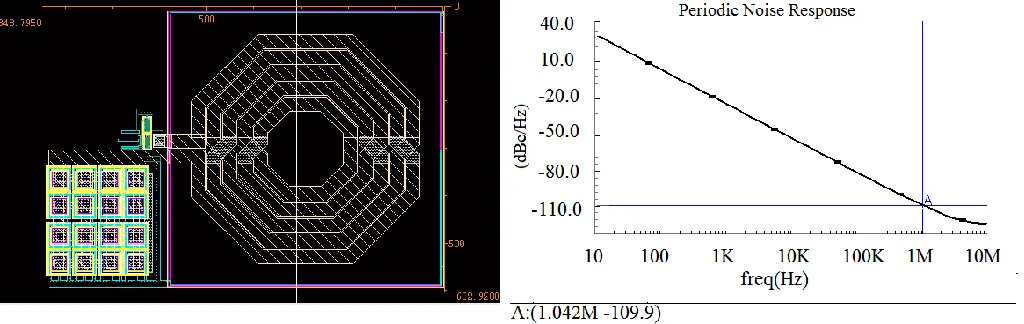
The proposed transmitter has been designed on a 0.18µm CMOS process. The oscillator has a 430MHz output signal. In Fig. 6, waveform of output modulated signal is shown with 1010 data message and 50 Mbps data rate frequency. The oscillator consumes 2 mA from the 1 volt power supply. Fig. 8 shows that the proposed transmitter has 0.85 mm×0.6 mm area without pads. Fig. 9 shows phase noise of transmitter output. Phase noise of TX is -109 dBc/Hz (beyond 1 MHz offset). The performance comparison with other low power transmitters is shown in Table II. In the proposed transmitter, FOM is 42 pJ/(bit×mw). The designed transmitter performs favorable compared with other reported transmitters.
Matching Block Vdd
Mp
Mn
50 RF Input
Antenna
Fig. 5. The circuitry of power amplifier
Matching Block Vdd
50 Antenna Vdd
Vdd Vdd Vdd1
Msw
Msw Message
Data
Power Amplifier Oscillator
Fig. 6. Circuit diagram of the complete proposed transmitter
Fig. 7. Waveform of output modulated signal is shown with 1010 data message and 50 Mbps data rate
TABLE I
SUMMARIZES OF CHARACTERISTIC OF TRANSMITTER
Parameters Value
Power supply (V) 1
Technology (µm) 0.18
Modulation OOK
Maximum Data Rate (Mbps) 60
Carrier Frequency (MHz) 430
Power consumption (mW) 2.3
Output Power (mW) 0.918
Fig. 8. Layout of the transmitter Fig. 9. Phase noise of the transmitter
TABLE II
PERFORMANCE COMPARISON OF TX
Reference 10 13 9 11 12 This work
Fcarrier 2.4 2.46 0.44 0.433 2.4 0.43
Technology(µm) 0.13 0.18 0.35 0.35 0.18 0.18
Data Rate (Mbps) 0.3 136 40 10 4 60
Modulation FSK OOK OOK OOK OOK OOK
Power Supply (v) 0.6 1.5 3 1 1.8 1
Pdc(mW) 1 3 2.58 0.518 2 2.3
Output Power(mW) 0.3 0.04 0.951 0.0537 5.857 0.9182
FOM (pJ/(bit×mW) 11111 551 68 965 651 42
I. CONCLUSION
A highly efficient OOK transmitter has been proposed for wireless body sensor network. The transmitter chip has been designed in 0.18 μm CMOS process. DCO, modulator and power amplifier compose OOK transmitter with 60 Mbps maximum data rate. The proposed transmitter requires 1-volt supply voltage. In the proposed TX, data rate is not limited by startup time of the oscillator. The proposed TX occupies small area and FOM of TX is 42 pJ/(bit×mW).The proposed high efficiency transmitter is well suited for high data rate monitoring of biomedical signals.
REFERENCES
[1] A. W. Wong, D. McDonagh, G. Kathiresan, O. Omeni, O. El-Jamaly, T. K. Chan, P. Paddan, and A. Burdett, “A 1 V, micropower system-onchip for vital-sign monitoring in wireless body sensor networks,” in Proceeding IEEE International. Solid-State Circuits Conference, 2008, pp. 138–139.
[2] Y. J. Yang, Y. J. Huang, H. H. Liao, T. Wang, P. L. Huang, C. W. Lin, Y. H. Wang, and S. Lu, “A release-on-demand wireless CMOS drug delivery soc based on electro thermal activation technique,” in Proc. IEEE International Solid-State Circuits Conference, 2009, pp. 288–289. [3] M. Vidojkovic1 et al., “A 2.4GHz ULP OOK Single-Chip Transceiver for Healthcare Applications,” IEEE International Solid-State Circuits Conference, (ISSCC), 2011, pp. 458-460.
[5] B. Razavi,’’ A Study of Phase Noise in CMOS Oscillators “ IEEE journal of solid-state circuits, Vol. 31, No. 3, pp.331-343,1996 [6] A. Hajimiri, S. Limotyrakis, and T. H. Lee,” Jitter and Phase Noise in
Ring Oscillators “IEEE journal of solid-state circuits, Vol. 34, No. 6, pp.790-804, 1999.
[7] J. P. Carmo, N. Dias, P. M. Mendes, C. Couto, Helder Raul Silva,and J. H. Correia, “A 2.4-GHz Low-Power/Low-Voltage Wireless Plug-and-Play Module for EEG Applications” IEEE Sensors Journal, Vol. 7, pp. 1524 – 1531, 2007.
[8] R. Jiho; K. Minchul, Lee, Jaechun; Kim, Byung-Sung; Lee, M-Q Nam, and S wook, “Low Power OOK Transmitter for Wireless Capsule Endoscope,” IEEE/MTT-S International Microwave Symposium, 2007. [9] D. C. Daly and A P Chandrakasan, “An energy-efficient OOK
transceiver for wireless sensor networks,” IEEE Journal Solid-State CircuitsVol. 42, No. 5, pp. 1003–1011, 2007.
[10] Ben W. Cook et, ”An Ultra low Power 2.4GHz RF Transceiver for Wireless Sensor Network in 0.13 µm CMOS with 400mw supply and an Integrated Passive RX front-End,” in IEEE ISSCC dig. Tech. Papers, 2006, pp.1460-1469.
[11] M. K. Raja and Y. P. Xu, ” A 52 pJ/bit OOK Transmitter with adaptable data rate,” in Proc Solid-State Circuits Conference, 2008. IEEE Asian / Fukuoka, Japan 3-5, pp. 341 –344.
[12] Z. Qi, K. Xiaofei and W. Nanjian, “An ultra-low-power RF transceiver for WBANs in medical applications,” Journal of Semiconductors, Vol. 32, No. 6. 2011.
student in Faculty of Electrical and Computer Engineering, University of Tabriz, Tabriz, Iran.
Ziaadin Daie Koozekanni received his PhD degree in Electrical Engineering
from the Brunel University of West London, UK in 1996. He has been teaching as an assistant professor in University of Urmia from 1996 to 2004 and in University of Tabriz since 2004. At the time being he works as an associate professor in Faculty of Electrical and Computer Engineering, University of Tabriz and his position is Dean of ECE faculty. His current scientific interests are analog integrated circuit design, Data Converters, RF IC Design and Optical Filter Design.
Jafar Sobhiwas born in Tabriz, Iran. He received B.S. degree in electrical engineering from University of Tabriz, Iran. He received M.Sc and Ph.D degree in electrical engineering from University of Urmia. His research interests are high-speed high-resolution Data converter design, mixed signal circuits design and RF integrated circuits design. He is currently with Faculty of Electrical and Computer Engineering, University of Tabriz, Tabriz, Iran.
Nasser Nasirzadeh Azizkandi received in B.S. degree in electrical