Structural Analysis of InGaAs Based
Vertical Cavity Surface-Emitting Quantum
Well Laser
M. M. BISWAS†,*, M. M. HOSSAIN††,↨, S. NURUDDIN††, K. K. DAS†, M. A. H SADI† †Department of Electrical & Electronic Engineering, Stamford University Bangladesh
51 Siddeswari Road, Dhaka-1217, Bangladesh
††Department of Electrical & Electronic Engineering, Khulna University of Engineering & Technology
Khulna-9203, Bangladesh
Abstract:
This paper describes the theoretical design of multiple quantum well (MQW) vertical cavity surface emitting laser (VCSEL) on ternary In0.31Ga0.69As substrate. The 1.3 µm wavelength laser is designed considering the
DBR reflectivity, number of quantum wells in the active region and dimension of tunnel junction (TJ). The minimum threshold current density is found to be 84.04 Acm-2 when the number of quantum well is five. The
optimum thickness of the tunnel junction (TJ) is estimated to be 12 nm to yield low free carrier absorption (FCA) loss and maximum tunneling probability. The results indicate that the proposed InGaAs-based quantum well laser is the promising one for the fabrication of high performance laser.
Keywords: VCSEL; DBR; multiple quantum well; threshold current; tunneling probability; free carrier absorption loss.
1. Introduction
The ternary compound semiconductor InxGa1-xAs is a promising material for advanced optoelectronic devices
because its lattice constant can be changed according to the requirements. The potential applications of compositionally homogeneous bulk InxGa1-xAs single crystals are found to be as substrate for InGaAs-based
laser diode [1]. Conventional 1300 nm lasers are based on the InGaAsP or InGaAlAs quantum-well (QW) active material system on an InP substrate. Unfortunately, these 1300 nm InP-based diode lasers suffer poor lasing performance at high temperature operation [2]. However, due to the lattice mismatch between the substrate and epilayer, desired performances are not found for these laser diodes. Especially the gain characteristics as well as temperature characteristics of such lasers are poor [3]. The characteristics temperature (T0) of InGaAs ternary
substrate based laser is 150 K which is comparably higher than InP-based laser [4].
VCSELs have a number of advantages over conventional edge emitting lasers. Simpler in processing, emission in a single longitudinal mode naturally, lower divergence, and preparation in the form of large and planar arrays which is suitable for parallel optical signal processing. A further advantage of the VCSEL is its relatively small cross-sectional area, which minimizes the operating current [5].
From above discussions it is clear that temperature effect, operating current, and lattice matching conditions play important roles on the performance of the laser. The measured room-temperature threshold current density of the InGaAs QW lasers was found to be 90 Acm-2 at an emission wavelength of 1233 nm [6]. However, it is
2. Device Structure
The performance of a laser greatly depends upon the materials and dimensions of the active layer, Bragg reflector, and tunnel junction. The top emitting VCSEL structure is shown in Fig. 1.
The active region contains 8 nm thick undoped In0.42Ga0.58As quantum wells, separated by 11 nm thick
In0.26Ga0.74As barrier layers. In0.24Ga0.76As cladding layer is used to sandwich the active region. A
p-InAlGaAs/n-InAlGaAs tunnel junction is introduced for electrical and optical confinement. The band gap energy for active layer, barrier layer, and cladding layer are 0.870 eV, 1.062 eV and, 1.090 eV respectively.
3. Calculation Method
Theoretical analysis for the proposed QWL structure is focused mainly on DBR reflectivity, number of quantum wells in the active region, and dimension of tunnel junction (TJ).
3.1. Distributed Bragg Reflector Design
A distributed Bragg reflector (DBR) consists of a quarter-wave length thick layer mirror. In order to ensure low threshold operation in long-wavelength VCSEL devices, both DBRs are required to provide power reflectivity of performance of greater than 99%. In fact, the high reflectivity DBR should provide a reflectivity greater than 99.9% and the low reflectivity (output) DBR should be designed to provide ≈ 99.5% in order to keep losses low enough for the devices to reach threshold [7]. Reflectivity (R) of the DBR is given by [8],
where nc, nh, nl,, and ns are the respective refractive indices of the cladding material, the two alternating
materials and the substrate and N is the number of repeated pairs of low/high refractive index material.
In order to optimize the distributed Bragg reflector (DBR) for the proposed VCSEL, In0.26Ga0.74As/Al0.90Ga0.10As, In0.26Ga0.74As/Al0.80Ga0.20As and GaAs/Al0.90Ga0.10As material combinations are
selected. The compositions of the DBR materials are chosen to be In0.26Ga0.74As,Al0.90Ga0.10As, Al0.80Ga0.20As
and GaAs so that these are lattice matched to the substrate. The relative indices of these materials are 3.54, 2.97, 3.09 and, 3.45 respectively.
3.2. Active Region Design
Employing too few wells may result in insufficient material gain to sustain lasing at high temperatures [9]. Our goal is to choose the number of QWs which theoretically yields lower threshold current (Ith) at high temperature.
The material gain and absorption losses are related as [10],
(1)
Fig. 1. Basic device structure of the proposed top emitting VCSEL.
InGaAs Substate
InGaAs MQW
active region
p-InAlGaAs/n-InAlGaAs
Tunnel junction aperture
InGaAs/AlGaAs
DBRs
∑ , ∑ , (2)
where is the gain enhancement factor, Lw is the well thickness, Nw is the number of well, gth is the threshold
gain, Rt and Rb are the top and bottom mirror reflectivity respectively. Lcis the cavity length, NiLi refers the total
length of the active region which consist total wells and barriers, αi andαc are the absorption losses in the active
and cladding layers respectively. The expression of is given by [10],
1 ; ∑ , (3)
where,σ represents total active region/wavelength. The absorption loss in the active region is assumed to be lower than the gain. The most important parameter for the design is the threshold current density which is related to the threshold gain as [11],
(4)
where q is the charge of electron, τ carrier lifetime, C is Auger recombination coefficient, d is the active region width, and its value is given by ∑w,hNiLiand nthis threshold carrier density which can be calculated from
threshold gain by nth=(8πv02gthτ∆vnr2)/c2; v0 is the emission light frequency, ∆v is the line width of the laser
frequency spectrum, nr is the refractive index of the active region, c is the velocity of light.
3.3. Tunnel Junction Optimization
Recent research is devoted to the tunnel junction (TJ) structures incorporated into long-wavelength vertical-cavity surface-emitting lasers (LW-VCSELs) in order to realize reduced optical loss, as well as increasing current and optical confinement. The tunnel junction provides enough lateral spreading resistance to uniformly spread carriers into the active region which is most important for single mode VCSEL [9]. The depletion layer in the tunnel junction is expressed as [11]
√ | | (5)
where Vbi is the built in potential, εs is the static dielectric constant of TJ material, NA is the acceptor
concentration and ND is the donor concentration. For the parabolic energy barrier the tunneling probability Tt can
be given by the WKB approximation [12],
/ /
√ ħ (6)
where ξis the average electric field of a step junction and it can be given as [12],
(7)
where qVbi is the built-in potential energy, is the static dielectric constant of the TJ material, and N*is the
effective doping concentration,
. (8)
The built in potential is expressed as [12],
(9)
where a is the impurity gradient in cm-4, n
i is the intrinsic carrier density, and W is the total depletion width In
TJ the single pass optical loss is given by [13],
where L = Ln + Lp ; Lnand Lp are the thicknesses of the n and p sides of the junction respectively, αiis the
internal optical loss from free carrier absorption (FCA).
4. Results
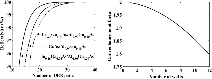
This section describes the performance of the proposed InGaAs-based 1.33 μm VCSEL. Fig. 2. shows the percentage variation of reflectivity with the number of DBR pairs for different material compositions at 1300 nm. Since the bandgaps of In0.26Ga0.74As and Al0.90Ga0.10As are 1.06 eV and 2.11 eV, the probability of emission
light absorption is low for In0.26Ga0.74As/Al0.90Ga0.10As DBR pairs. Again, from Fig. 2, it seen that the
reflectivity is obtained from small number of the In0.26Ga0.74As/Al0.90Ga0.10As DBR pairs due to its higher
refractive index contrast than In0.26Ga0.74As/Al0.80Ga0.20As and GaAs/Al0.90Ga0.10As DBRs. Therefore the
In0.26Ga0.74As/ Al0.90Ga0.10As mirror is chosen for the proposed VCSEL. For this mirror, the reflectivity of 0.999
and .995 are found for the 24 and 20 pairs and mirrors with these values of reflectivity are used as bottom and top mirror, respectively.
According to (2), number of quantum well and gain enhancement factor should be higher to obtain lower threshold gain. But it is not possible simultaneously because as the number of quantum well increases the value of gain enhancement factor also decreases as shown in Fig. 3.
Threshold current density is calculated using (2), (3) and (4) and is shown in Fig. 4. It is found that for any value of mirror reflectivity, the threshold current decreases with increasing the number of well until it reaches at minimum value and remain approximately constant for increasing one or two wells and again it increases. This is because, with increasing the number of wells the gain enhancement factor decreases and the material gain
Fig. 3.Dependence of gain enhancement factor on number of quantum well in the active region.
0 2 4 6 8 10 12
1.75 1.8 1.85 1.9 1.95 2
Number of wells
G a in en h a n cem en t f a c tor
Fig. 2. DBR reflectivity vs. number of pairs for various materials combinations at 1300 nm.
10 20 30 40
95 96 97 98 99 100
Number of DBR pairs
R e fl e c ti v ity (% )
In0.26Ga0.74As/Al0.80Ga0.20As In0.26Ga0.74As/Al0.90Ga0.10As
GaAs/Al0.90Ga0.10As
Fig. 5. Variation of tunneling probability as a function of deplition width of the n-InAlGaAs/p-InAlGaAs tunnel junction.
0 10 20 30
0.96 0.97 0.98 0.99 1
Depletion width ( nm)
T u n n elin g p r o b ab ility
T = 300 K T = 310 K T = 320 K
T = 330 K
Fig. 4. Threshold current density as a function of number of quantum wells in the active region for different DBR reflectivity.
0 2 4 6 8 10 12
100 150 200 250
Number of wells
T h resh o ld cu rren t d e n si ty ( A cm -2 )
R = 0.990
R = 0.993
increases. Due to the combined influence of the gain enhancement factor and the material gain, initially the threshold current decreases rapidly and reaches to it minimum value for the number of wells five and then it increases gradually with number of wells. For the top mirror reflectivity 0.995 the threshold current density is evaluated to be 84.04 Acm-2for the number of wells five. Hence, in our proposed VCSEL, five quantum wells
are used in the activeregion.
Variation of tunneling probability as a function of depletion width of the n-InAlGaAs/p-InAlGaAs tunnel junction is shown in Fig. 5. The tunneling probability decreases with increasing depletion width. This occurs when temperature decreases, because with the decrease of temperature the bandgap energy increases. The TJ width should be small for achieving large tunneling probability.
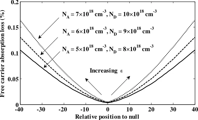
Fig. 6 shows that FCA loss increases for shifting to the optical standing-wave null in relative position of the tunnel junction (TJ). The FCA loss also increases with the increase of doping densities, since αi increases with
the increase in doping densities. However, higher doping densities are required to minimize the thickness of TJ [9]. So there must be a compromise between these two opposite conditions. By taking the donor and acceptor concentration as 8x1018 cm-3 and 5x1018 cm-3 respectively, depletion width of 9.42 nm has been evaluated. The
TJ needs to be thick enough as not to deplete the layers, but as thin as possible to minimize free-carrier optical absorption [14]. Since the depletion width is calculated to be 9.42 nm, so the thickness of the TJ of 12 nm has been taken to yield low free carrier absorption (FCA) loss and maximum tunneling probability.
5. Conclusions
A theoretical design has been presented of InGaAs- based 1.3 µm vertical cavity surface emitting laser (VCSEL). The design has been optimized by considering the thickness of quantum well and barrier, the number of quantum wells, threshold current, DBR reflectivity, TJ thickness, and different losses. The lowest threshold current density is calculated to be 84.04 Acm-2 for five wells in active layer. The 12 nm thick
InAlGaAs/InAlGaAs tunnel junction is optimized which exhibits less FCA loss and high tunneling probability. The proposed structure has been successfully designed with acceptable enhanced results which will create a way to fabricate InGaAS based VCSEL.
References
[1] K. Otsubo, Y. Nishijima, T. Uchida, H. Shoji, K. Nakazima, and H. Ishikawa, “1.3 μm InGaAs/ InAlGaAs strained quantum well lasers on InGaAs ternary substrates,” Jpn. J. Appl. Phys., vol. 38, p.p L312-L314, March 1999.
[2] N. Tansu, Jeng-Ya Yeh, and L. J. Mawst, “Extremely low threshold-current-density InGaAs quantum-well lasers with emission wavelength of 1215–1233 nm,” Appl. Phys. Lett., vol. 82, no. 23, Jan. 2003.
[3] M. Kaneko, S. Nakayama, K. Kaswiwa, S. Aizawa, and N. S. Takahashi, “Lattice Mismatched LPE Growth of InGaP on Patterned InP Substrate,” Cryst. RES Technol., vol. 37, no. 2-3, pp. 177-182, Feb. 2002.
-400 -30 -20 -10 0 10 20 30 40
0.05 0.1 0.15 0.2
Relative position to null
F
r
ee
car
r
ie
r ab
so
rp
ti
on
l
o
ss
(
%
)
NA = 7×1018 cm-3, ND = 10×1018 cm-3
NA = 5×1018 cm-3, ND = 8×1018 cm-3
NA = 6×1018 cm-3, ND = 9×1018 cm-3
Increasing
[4] K. Otsubo,Y. Nishijima, and H. Ishikawa, “Long- wavelength Semiconductor Lasers on InGaAs ternary substrates with excellent temperature characteristics,” Fujitsu Sci. Tech. J., vol. 34, no. 2, pp. 212-222, Dec. 1998.
[5] J. Orton, The Story of Semiconductors, Oxford University, 2004.
[6] N. Tansu, Jeng-Ya Yeh, and L. J. Mawst, “Extremely low threshold current-density InGaAs quantum-well lasers with emission wavelength of 1215–1233 nm,” Appl. Phys. Lett., vol. 82, no. 23 June 2003.
[7] D. F. Feezell, “Long-Wavelength Vertical-Cavity Surface-Emitting Lasers with Selectively Etched Thin Apertures,” University of California, Santa Barbara,163 pages, 3187229, Sep. 2005.
[8] L. A. Coldren and S. W. Corzine, Diode Lasers and Photonic Integrated Circuits, New York, NY: Wiley, 1995.
[9] M. Mehta, “High-Power, High-Bandwidth, High-Temperature Long-Wavelength Vertical-Cavity Surface- Emitting Lasers,” University of California, Santa Barbara, 3218873,June 2006.
[10] K. Uomi, S. J. B. Yoo, A. Scherer, R. Bhat, N. C. Andreadakis, C. E. Zah, M. A. Koza, and T. P. Lee, “Low threshold, Room temperature Pulsed Operation of 1.5-μm Vertical Cavity Surface Emitting Lasers with an Optimized Multi-Quantum Well Active layer,” IEEE Photonics Tech. Lett., vol. 6, no. 3, March 1994.
[11] P. Bhattacharya, Semiconductor Optoelectronic Devices, Pearson Prentice Hall, 2006. [12] S. M. Sze, Physics of Semiconductor Devices, Wiley, New York, 1981.
[13] D. Feezell, D. A. Buell, D. Lofgreen, M. Mehta, and L. A. Coldren, “Optical Design of InAlGaAs Low-Loss Tunnel-Junction Apertures for Long-Wavelength Vertical-Cavity Lasers,” IEEE Journal of Quantum Electronics, vol. 42, no. 5, May 2006.
[14] N. Margalit, "High-Temperature Long-Wavelength Vertical-Cavity Lasers," University of California, Santa Barbara, 1998.
Authors Photograph and Biography
Md. Multan Biswas received the Bachelor of Science (B. Sc.) degree in Electrical & Electronic
Engineering (EEE) from Khulna University of Engineering & Technology (KUET) in 2009. He is now with the Department of EEE at Stamford University Bangladesh as a lecturer. Besides he is continuing his M. Sc. in Electrical Energy and Power Systems group in the department of EEE at Bangladesh University of Engineering & Technology (BUET), Bangladesh. He has some publications in international journals and conferences. He is an associate member of Institution of Engineers, Bangladesh (IEB). His present research interests are in the fields of Power Systems, Power Electronics Converters, Renewable Energy, and Energy Storage Systems.
Md. Mottaleb Hossain received the Bachelor of Science (B. Sc.) degree in Electrical & Electronic
Engineering (EEE) from Khulna University of Engineering & Technology (KUET), Bangladesh in 2009. He is involved in research on Laser applications, Optics, Nanophotonics, and Quantum Electronics. He has several publications in peer reviewed journals and conferences in the relevant fields. He is a Graduate Student Member of IEEE. He is also a member of IEEE EDS, IEEE Photonics Society, SPIE, IACSIT, and IEB. Recently he has been selected as a reviewer of IACSIT. He is now with the Department of EEE at Stamford University Bangladesh as a lecturer.
Shaikh Nuruddin received the Bachelor of Science (B. Sc.) degree in Electrical & Electronic Engineering (EEE) from Khulna University of Engineering & Technology (KUET) in 2009. His research interests are in the fields of Power Systems, Power Electronics, Renewable Energy, and Energy Storage Systems. He is an associate member IEB. He is now with the SINHA Power Generation Company Limited, Bangladesh as a Junior Engineer (Electrical).
Kamol Kanto Das received the Bachelor of Science (B. Sc.) degree in Electrical & Electronic Engineering (EEE) from Rajhshahi University of Engineering & Technology (RUET) in 2009. He is involved is reserch on Power systems, Neural Networks, Optoelectronics, Control systems, and Robotics. He is an associate member of Institution of Engineers, Bangladesh (IEB). He is now with the Department of EEE at Stamford University Bangladesh as a lecturer.