LETTER
MEMS capacitive pressure sensor
monolithically integrated with CMOS readout
circuit by using post CMOS processes
Munseon Jang and Kwang‑Seok Yun
*Abstract
In this paper, we presents a MEMS pressure sensor integrated with a readout circuit on a chip for an on‑chip signal processing. The capacitive pressure sensor is formed on a CMOS chip by using a post‑CMOS MEMS processes. The proposed device consists of a sensing capacitor that is square in shape, a reference capacitor and a readout circuitry based on a switched‑capacitor scheme to detect capacitance change at various environmental pressures. The readout circuit was implemented by using a commercial 0.35 μm CMOS process with 2 polysilicon and 4 metal layers. Then, the pressure sensor was formed by wet etching of metal 2 layer through via hole structures. Experimental results show that the MEMS pressure sensor has a sensitivity of 11 mV/100 kPa at the pressure range of 100–400 kPa.
Keywords: Pressure sensor, Capacitive sensor, Post‑CMOS, MEMS sensor, CMOS MEMS
© The Author(s) 2017. This article is distributed under the terms of the Creative Commons Attribution 4.0 International License (http://creativecommons.org/licenses/by/4.0/), which permits unrestricted use, distribution, and reproduction in any medium, provided you give appropriate credit to the original author(s) and the source, provide a link to the Creative Commons license, and indicate if changes were made.
Background
As the technologies of micro electromechanical systems (MEMS), micromachining, and nano-processes have been advanced, it becomes more important to accurately con-trol and process the noisy signal from the MEMS-based precise sensors, improve the performance, reduce cost, and finally realize the system-on-chip concept [1]. These benefits could be obtained by the monolithic integration of MEMS sensors with electronics, which has been applied to commercially available products such as accelerometers, bolometers, digital mirror displays, and so on [2–5].
The fabrication of MEMS structures using standard complementary metal oxide semiconductor (CMOS) device with minimal post processes has been exploited for several years, enabling the monolithic integration of MEMS structures and signal processing circuitry with just a few further steps after the CMOS process [6, 7]. To date, various CMOS–MEMS devices have been implemented by using post-CMOS process such as iner-tial sensors, magnetometers and pressure sensors, etc. [8–11].
The capacitive MEMS pressure sensors are one of the most widely used transducers of the various types of MEMS pressure sensors since they offer excellent noise performance, low power consumption, and easy integra-tion with processing circuitry [9, 10, 12]. Narducci et al. reported a capacitive pressure sensor using aluminum metal layers of a commercial CMOS process as sensing electrodes [10]. Cheng et al. improved the sensitivity by using multiple metal layers to form mechanical structure of a CMOS-based pressure sensor [9].
In this paper, we present the fabrication of a capaci-tive pressure sensor based on post-CMOS process and its characterization by using monolithically integrated circuitry.
Design Pressure sensor
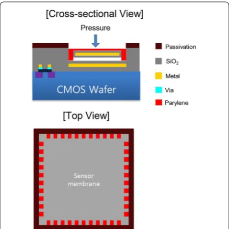
Figure 1 shows the top and cross-sectional view of the proposed pressure sensor having diaphragm in square shape. The electrodes for the capacitive sensor were formed by the aluminum layers. The top electrode was supported by the silicon dioxide and Parylene lay-ers. When an external pressure is applied to the sensor membrane, the gap distance between two metal elec-trodes decreases. Then, the pressure can be monitored
Open Access
*Correspondence: [email protected]
by measuring the capacitance between the electrodes through on-chip circuitry.
The mechanical properties of the materials compos-ing diaphragm are listed in Table 1. In this work, the target pressure range is around 100–500 kPa which is general pressure range for vehicle applications, bio medi-cal devices, and some industrial applications such as tire pressure monitoring, blood pressure measurement, and pneumatic control equipments. To operate the sensor in those pressure ranges, the side length of the square mem-brane is designed as 56 μm. The resonance frequency calculated with these membrane dimensions is about 1.3 MHz, which is high enough for the pressure sensor in most applications [14]. We designed total 9 capacitors in parallel connection to have initial capacitance value of 200 fF.
Readout circuit
The readout circuit for the proposed capacitive pres-sure sensor is based on a switched-capacitor scheme
employing reference capacitors and sensing capacitors. We used fully differential scheme to suppress a signal drift by temperature variation and an error caused by the capacitance mismatch between reference and sensing capacitors.
Figure 2 shows the sample-hold circuit and its timing diagram to measure the capacitance of sensing capacitor. Then, the output voltage is given by
where Vin− and Vin+ are input voltage on negative and posi-tive terminal, Vout+ and Vout− are output signal from positive and negative output terminal, and Cs and Cref are sensing and reference capacitance, respectively.
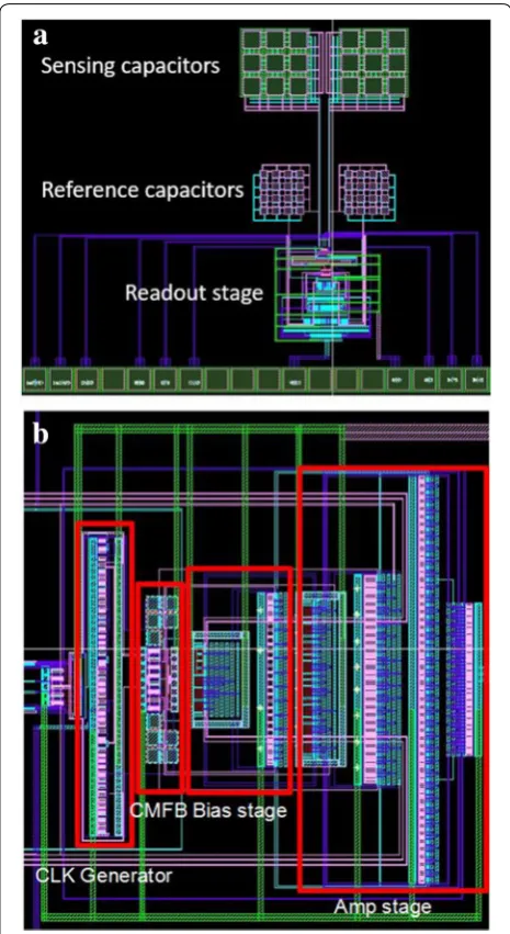
Figure 3 shows a layout of the entire chip and magni-fied view of the processing circuit. The reference capaci-tor formed by nine capacicapaci-tors in parallel connection is designed to have a capacitance of 128 fF. The processing (1)
V+
out−V
−
out Vin−−Vin+ =
Cs Cref
,
Fig. 1 Cross‑sectional and top view of the proposed pressure sensor
Table 1 The mechanical properties of the materials com-posing diaphragm
Material Thickness
(μm) Young’s modulus (GPa) Poisson’s ratio
SiO2 0.85 69 0.17
Aluminum 0.7 70 0.3
Parylene 1.5 3.2 0.4
Fig. 2 a Sample‑hold circuit to measure the sensing capacitance.
circuit is composed of amplifier, clock generator, and common-mode feedback (CMFB) biasing stage [7, 13].
Fabrication
The CMOS chip was fabricated by using commer-cial foundry of 0.35 μm 2P4M (2 Poly silicon, 4 metal) process. The conductive materials for signal line and via is aluminum and tungsten, respectively. Figure 4
shows the process flow to fabricate the pressure sen-sor using post-CMOS process. Figure 4a depicts the cross-section and top view of the capacitive sensor after the CMOS process. The metal 3 and metal 1 form the top and bottom electrodes for the sensing capaci-tor, respectively, and metal 2 is used as a sacrificial layer. Next, the via and metal 2 layer are removed by using wet etching as shown in Fig. 4b. The etchant was a mixture of H2SO4 and H2O2 in the volume ratio of 2 to 1. Finally, the via holes are sealed by the deposition of Parylene C.
Results and discussions
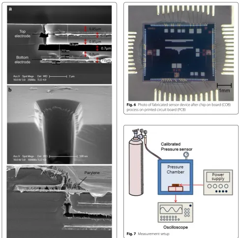
Figure 5 shows the SEM image of the sensing capacitor after etching of metal 2 as a sacrificial layer. The gap dis-tance is about 0.7 μm. In the magnified view of via region in Fig. 5b, we could verify that the sacrificial metal lay-ers in via and metal 2 have been clearly removed while the top and bottom metal layers were not damaged by the etchant. Figure 5c is the SEM image after Parylene depo-sition, where the via hole is completely sealed.
Figure 6 shows the photo of fabricated sensor device after chip on board (COB) process on printed circuit board (PCB). The die dimension is 4 mm × 5 mm. The sensor characteristic was measured in a pressure chamber where the pressure was regulated by using a pressurized air tank and a calibrated pressure gauge as shown in Fig. 7. The out-put signal was measured through an oscilloscope. The bias voltage on VDD terminal is 3.3 V. Also, the voltages on Vin+, Fig. 3 a Layout of the entire chip and b magnified view of the
processing circuit stage
V−in, and Vcmo are 1.7, 1.3, and 1.5 V, respectively, to have 1.45 V of a common-mode voltage at the sample and hold stage.
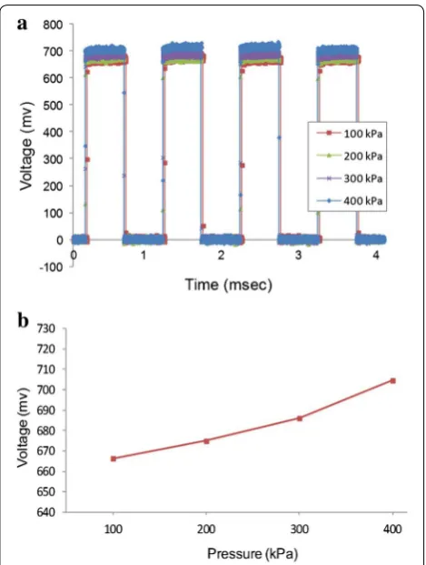
The real time output signals at various pressure differ-ences are shown in Fig. 8a. As the pressure increases, the peak voltage of output signal also increases. As shown in Fig. 8b describing the output signal (Vout+ − Vout−) versus pressure, the proposed sensor is quite linear in the pres-sure range from 100 to 400 kPa. The sensitivity of the fab-ricated device was about 11 mV/100 kPa.
Fig. 5 a SEM image of the sensing capacitor after sacrificial layer etching , b magnified view of via hole, and c after Parylene C deposi‑ tion
Fig. 6 Photo of fabricated sensor device after chip on board (COB) process on printed circuit board (PCB)
Conclusions
In this paper, we reported the fabrication of capacitive pressure sensor using post-CMOS process and measured its response at various applied pressures. The capacitive sensor was monolithically integrated with the CMOS cir-cuitry processed by 0.35 μm foundry process to minimize the parasitic capacitance and electromagnetic interfer-ence noise. The readout circuit of fully differential struc-ture based on switched-capacitor scheme was used to monitor the change of the sensing capacitor. The sensi-tivity of the fabricated sensor was 11 mV/100 kPa in the operation range of 100 to 400 kPa. As a future work, the integration of analog to digital converter and signal min-ing stage is required to improve the sensitivity and noise performance.
Authors’ contributions
MJ participated in design, fabrication, and test the device and drafted the manuscript. KSY conceived of the study, reviewed all test methods and results, and finalized the drafted manuscript. Both authors read and approved the final manuscript.
Competing interests
The authors declare that they have no competing interests.
Funding
This research was supported by the MSIP (Ministry of Science, ICT and Future Planning), Korea, under the ITRC (Information Technology Research Center) support program (IITP‑2016‑H8501‑16‑1010) supervised by the IITP (Institute for Information & communications Technology Promotion), the National Research Foundation of Korea (NRF) grant funded by the Korea government (MSIP) (2016R1A2B4014629), and IDEC (IC Design Education Center).
Received: 23 November 2016 Accepted: 28 December 2016
References
1. Chavan AV, Wise KD (2002) A monolithic fully‑integrated vacuum‑sealed CMOS pressure sensor. IEEE Trans Electron Devices 49(1):164
2. Luo H, Fedder GK, Carley LR (2000) A 1 mG lateral CMOS–MEMS acceler‑ ometer. Proceedings IEEE thirteenth annual international conference on micro electro mechanical systems (Cat No00CH36308), p 502–507 3. Niklaus F, Vieider C, Jakobsen H (2008) MEMS‑based uncooled infrared
bolometer arrays: a review. In: Proceedings SPIE, vol 6836. MEMS/MOEMS Technologies and Applications III, Beijing. doi:10.1117/12.755128 4. Hornbeck LJ (2001) The DMDTM projection display chip: a MEMS‑based
technology. MRS Bull 26(04):325
5. Tsai M‑H, Liu Y‑C, Fang W (2012) A three‑axis CMOS–MEMS accelerometer structure with vertically integrated fully differential sensing electrodes. J Microelectromech Syst 21(6):1329
6. Kim JW, Takao H, Sawada K, Ishida M (2007) Integrated inductors for RF transmitters in CMOS/MEMS smart microsensor systems. Sensors. 7(8):1387
7. Chang SP, Allen MG (2004) Demonstration for integrating capacitive pressure sensors with read‑out circuitry on stainless steel substrate. Sens Actuators A: Phys. 116(2):195
8. Fedder GK (2005) CMOS‑based sensors. In: IEEE sensors conference 2005 9. Cheng C‑L, Chang H‑C, Chang C‑I, Fang W (2015) Development of a
CMOS MEMS pressure sensor with a mechanical force‑displacement transduction structure. J Micromech Microeng 25(12):125024 10. Narducci M, Yu‑Chia L, Fang W, Tsai J (2013) CMOS MEMS capacitive
absolute pressure sensor. J Micromech Microeng 23(5):055007 11. Hui Y, Nan T, Sun NX, Rinaldi M (2015) High resolution magnetometer
based on a high frequency magnetoelectric MEMS–CMOS oscillator. J Microelectromech Syst 24(1):134
12. Ahn Y, Song S, Yun K‑S (2015) Woven flexible textile structure for wearable power‑generating tactile sensor array. Smart Mater Struct 24(7):075002 13. Liu Y‑C, Tsai M‑H, Tang T‑L, Fang W (2011) Post‑CMOS selective electro‑
plating technique for the improvement of CMOS–MEMS accelerometers. J Micromech Microeng 21(10):105005
14. Manwar R, Arjunan L, Ahmadi M, Chowdhury S (2015) Resonant fre‑ quency calculation of square diaphragms: a comparison. In: IEEE 6th latin American symposium on circuits & systems, p 1–4
Fig. 8 a Real time output signals for various pressure differences and