Design of Low Power Half Adder Using
Adaptive Voltage Level (AVL) Technique
Karthick S
1, Mahesh P
2, Aravindkumar R
3Assistant Professor, Dept. of ECE, Bannari Amman Institute of Tech, Erode, Tamilnadu, India 1
UG Student, Dept. of ECE, Bannari Amman Institute of Tech, Erode, Tamilnadu, India 2
UG Student, Dept. of ECE, Bannari Amman Institute of Tech, Erode, Tamilnadu, India3
ABSTRACT: In VLSI arithmetic circuits plays a important role. In this adder is one of the arithmetic circuits. In this
paper, the half adder is being designed by using adaptive voltage level (AVL) techniques. These design are used to reduce the power consumption compared to other conventional design. We can reduce the value of the total power dissipation by using adaptive voltage level at ground (AVLG) technology in which the ground potential is raised to reduce power consumption and adaptive voltage level at supply (AVLS) in which the supply potential is increased to reduce the power consumption. This paper represents how to control the power by using AVL technique. The Half adder design using AVL technique are compared to the conventional half adder design based on the power consumption, propagation delay, speed, layout area and number of transistor is preferred. Power consumption of the proposed design is measured and compared. The result shows that there is a reduction in power and transistor count for this proposed method. The circuit is simulated on Micro Wind 3.1 and DSCH in CMOS technology.
KEYWORDS: Half adder, AVL technique, Low Power, High Speed Transistor Count, VLSI
I.INTRODUCTION
In Very Large Scale Integration the increasing demand for low power consumption is increased. Adder is a combinational circuit in which it represents the smallest unit used for the addition in the digital system. The adder is not only used for the arithmetic calculation in many device processors but also used in the other part of the processor for address calculations table indices, and similar operations. In these the half adder is a simpler device compared to other adders. This combinational circuit is used for the addition of two binary digits which is used for push-pop logical operation. Although adders can be constructed for many numerical representations, such as binary-coded decimal or excess-3, the most common adders operate on binary numbers. In cases where two's complement or ones' complement is being used to represent negative numbers, it is trivial to modify an adder into an adder–subtractor. Other signed number representations require a more complex adder.
Fig 1: Logic Symbol of Half Adder
The XOR Gate is responsible for finding the sum without worrying about a carry. XOR works here because if A and B are the same, then it will return 0, and if the values are different (one is a 1, one is a 0), then it will return a 1. The AND Gate is there to handle the carry. If both A and B are 1, the XOR gate will return 0, but the AND gate will differentiate if it is (0, 0) or (1, 1) and have a carry value if it is the latter. Figure 1 shows the logic symbol of the half adder.
II.RELATED WORK
They are many papers that have published for reducing the power consumption of the arithmetic circuits such as full adder circuit and half subtractor. In these papers they have designed the circuit by using much logic design style such as Complementary Pass Transistor design style, Transmission Gate design style, Hybrid CMOS design style, Bridge design style and many. These designs are modified by using the adaptive voltage level technique which have two method such as adaptive voltage level at ground and adaptive voltage level at source based on the CMOS technology at different sizes. In these work they have many limitations which have been listed
a) The main limitation of these papers is they have designed the circuit by using the adaptive voltage level
technique only for the arithmetic circuit like half subtractor and full adder excluded the circuit for the half adder.
b) The other limitation of this work is about the usage of number of transistor. They had used more number of
transistors by using various design style. Due to increase in the number of transistor the reduction in power consumption would not be done up to the desired level of the technique.
c) Using this adaptive voltage level technique they had to use additional number of CMOS transistor in these
work by which it increase the transistor count and leakage current of the transistor.
d) The routed wires and compiled cells which had been used in this proposed design of the arithmetic circuit such
as full adder and half subtractor are more due to increase in the number of transistor used.
III.CONVENTIONAL HALF ADDER
Fig 2: Conventional Half Adder circuit design
Fig 3: Conventional Half Adder design layout diagram
Figure 2 shows the conventional half adder circuit design and figure 3 shows the layout of the Conventional half adder
IV.PROPOSED WORK
A. Half adder circuit using AVL technique:
In this Adaptive Voltage Level technique the power consumption can be reduced from the conventional half adder design. In order to reduce the power consumption an additional control circuit which can be used at the upper end of the circuit to bring down the supply voltage value .It would reduce power leakage on each transistor known as Adaptive Voltage Level at Supply (AVLS) technique.
Level at Ground (AVLG) technique. The complete effect of these techniques on the power consumption can be described as follows.
B. Half adder circuit using AVLG technique:
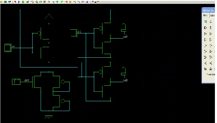
In Adaptive Voltage Level at Ground (AVLG) technique the additional control circuit consists of combination of 1-NMOS and 2-PMOS transistors which are connected in parallel. Additionally an input clock is applied at the input terminal of the NMOS transistor in the control circuit and the rest of the PMOS transistors in the control circuit are connected to the ground terminal. This AVLG control circuit is placed at the ground terminal of the conventional half adder circuit. It would lift the ground potential of the circuit to reduce the power consumption of the conventional half adder design. Depending upon the input the output also varied and the usage of clock is to prevent any defect in half adder function during power consumption.
Fig 4: Half adder design using AVLG technique
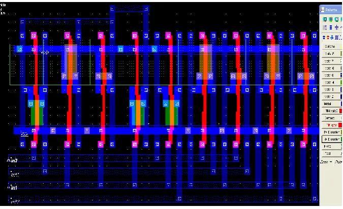
Figure 4 shows the half adder design using AVLG technique. The layout of this half adder design is simulated.
At VDD = 1.0 V the power consumption of this half adder design is 3.124 micro watt in 65 nm CMOS technology and the power consumption of this design on 90nm CMOS technology is about 6.741 micro watt. From this we can understood that the power consumption is reduced about 56% less when compared to the conventional half adder design.
C. Half adder circuit using AVLS technique:
In Adaptive Voltage Level at Supply (AVLS) technique the additional control circuit is made up of combination of 1 PMOS and 2 NMOS transistor connected in parallel. At which an input clock is applied at the input terminal of the PMOS transistor and the rest of the NMOS transistor is connected to the drain terminal. This AVLS control circuit is placed at voltage supply source terminal of the conventional half adder design in which supply is given through this control circuit. This control circuit at the upper end would bring down the supply voltage given to the whole circuit in order to reduce the power consumption of the conventional half adder design. When the input is varied corresponding output will be produced. It would reduce the leakage power by reducing the gate to source voltage and gate to drain voltage. This design would be responsible for very low power consumption.
Fig 6: Half adder design using AVLS technique
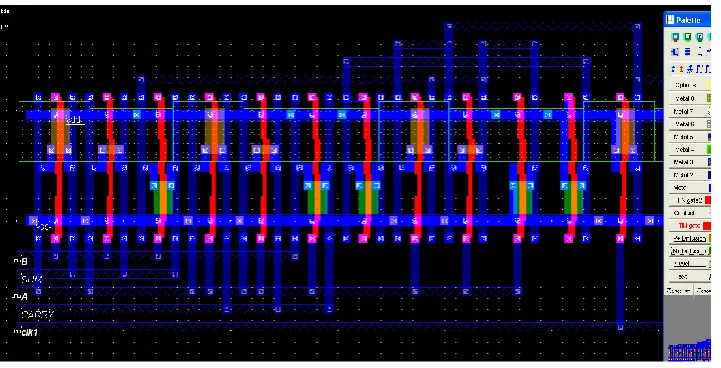
Fig 7: Layout design of half adder using AVLS technique
3.011 micro watt based on the 65nm CMOS technology. In 90nm CMOS technology the power consumption of this half adder design is about 6.406 micro watts. From this we can understand that the power consumption is reduced compared to the conventional half adder design. Compared to the AVLG technique in AVLS technique the power is reduced more efficiently.
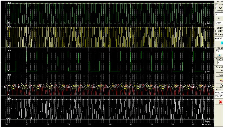
V.SIMULATION RESULTS AND WAVEFORMS
In this we have shown the simulated results of the power consumption, propagation delay, routed wires, speed and the compiled cells in the form of tabulation and also in the form of waveform we have shown the results.
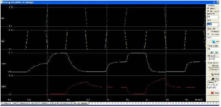
Fig 8: Simulated waveform of the conventional half adder design
Figure 8 shows the simulated waveform of the conventional half adder design and the figure 9 shows the simulation waveform of the half adder design using AVLG technique.
Fig 9: Simulated waveform of the half adder design using AVLG technique
Fig 10: Simulated waveform of the half adder design using AVLS technique
S.NO Parameters Conventional AVLG AVLS
1 Power consumption
(microwatt)
5.525 3.124 3.011
2 Routed wires 15 20 20
3 Compiled cells 6/6 9/9 9/9
4 Layout area
(micro meter square)
20.5 36.9 36.9
5 Propagation delay
(ps)
1.01 0.123 0.091
6 No .of PMOS &NMOS
transistors
3,3 5,4 4,5
Table 1: Comparison of the conventional half adder with half adder using AVLG & AVLS technique on 65 nm CMOS technology
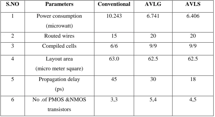
S.NO Parameters Conventional AVLG AVLS
1 Power consumption
(microwatt)
10.243 6.741 6.406
2 Routed wires 15 20 20
3 Compiled cells 6/6 9/9 9/9
4 Layout area
(micro meter square)
63.0 62.5 62.5
5 Propagation delay
(ps)
45 30 18
6 No .of PMOS &NMOS
transistors
3,3 5,4 4,5
Table 2: Comparison of the conventional half adder with half adder using AVLG & AVLS technique on 90 nm CMOS technology
VI. CONCLUSION
The simulation result of this half adder design using AVL technique shown that the power consumption is reduced. Various parameters which have been shown in the simulation result have influence on designing in VLSI design. In this the half adder design using AVL technique are generated in both 65nm and 90nm CMOS technology to know and study about various parameters like propagation delay and the power consumption. From this parameter we can understood that the optimized half adder is produced. When compared to the other technique the AVLS design of half adder is more efficient in speed, power consumption and leakage current. It also uses less number of routed wires compared to other design technique.
REFERENCES
[1] Tanvi Sood, Rajesh Mehra “Design a Low Power Half-Subtractor Using .90μm CMOS Technology” Volume 2, Issue PP 51-56 e-ISSN: 2319 – 4200, p-ISSN No. : 2319– 4197, 3 (May. – Jun. 2013).
[2] P. Divakara Varma, R. Ramana Reddy, “A Novel 1-Bit Full Adder Design Using DCVSL XOR/XNOR Gate and Pass Transistor Multiplexers”, International Journal of Innovative and Exploring Engineering (IJITEE), ISSN:2278-3075, vol. 2, Issue-4, March 2013. [3] Devendra Kumar Gautam, Dr. S R P Sinha, Er. Yogesh Kumar Verm Design a Low Power High Speed Full Adder Using AVL Technique
Based on CMOS Nano-Technology Volume 8, Issue 1 (Sep. - Oct. 2013).
[4] A.M.Shams, and M.A.Bayoumi, "A Novel High Performance CMOS 1Bit Full l Adder Cell" IEEE Transactions on Circuit and System, vol.47, NO.5, May, 2000.
[5] Y. Wang, Y. Jiang, and J. Wu, “Comprehensive power evaluation of full adders, ” Tech. Rep., Florida Atlantic Univ., Boca Raton, 2000. [6] T. Lynch and E. Swartzlander, “A spanning tree carry look ahead adder ,”IEEE Trans. Comput., vol. 41, pp. 931–939, Aug. 1992.