Multi-Functional Configurable Multiplier
1
K. Jagajivan & 2K.Naga Lavanya
1M.Tech Research Scholar, Priyadarshini Institute of Technology & Science, Chintalapudi 2Associate Professor, Priyadarshini Institute of Technology & Science, Chintalapudi
Abstract:
A multi-functional configurable multiplier optimized for low power and high speed operations and which can be configured either for single 8-bit multiplication operation, single 4-bit multiplication or twin parallel 8-bit multiplication is designed. The output product can be truncated to further decrease power consumption and increase speed by sacrificing a bit of output precision. Furthermore, the proposed multiplier maintains an acceptable output quality with enough accuracy when truncation is performed. Thus it provides a flexible arithmetic capacity and a tradeoff between output precision and power consumption. The approach also dynamically detects the input range of multipliers and disables the switching operation of the non effective ranges. Thus the ineffective circuitry can be efficiently deactivated, thereby reducing power consumption and increasing the speed of operation. Thus the proposed multiplier outperforms the conventional multiplier in terms of power and speed efficiencies.
Keywords:
Booth multiplier (BM);configurable multiplication; low-power
design; truncation; partially guarded
computation.
I. INTRODUCTION
Portable multimedia and digital signal processing (DSP) systems, which typically require flexible processing ability, low power consumption, and short design cycle, have become increasingly popular over the past few years. Many multimedia
and DSP applications are highly
multiplication intensive so that the performance and power consumption of these systems are dominated by multipliers. The computation of the multipliers manipulates two input data to generate many partial products for subsequent addition operations, which in the CMOS circuit design requires many switching activities. Thus, switching activity within the functional unit requires for majority of power consumption and also increases delay. Therefore, minimizing the switching activities can effectively reduce power dissipation and increase the speed of operation without impacting the circuit’s operational performance. Besides, energy-efficient multiplier is greatly desirable for many multimedia applications.
Here attempt is made to combine
configuration, partially guarded
to design a high speed and power-efficient configurable BM (CBM). The main concerns are speed, power efficiency and structural flexibility. The proposed multiplier not only perform single 8-b, single 4-b, or twin parallel 8-b multiplication operations but also offer a flexible tradeoff between output accuracy and power consumption to achieve more power savings.
Several techniques are available [1] – [3] to improve the speed and power efficiency is analyzed. Approaches termed guarded evaluation; clock gating, signal gating,
truncation etc. reduce the power
consumption and increase the speed of
multipliers by eliminating spurious
computations according to the dynamic range of the input operands. The work in [4] separated the arithmetic units into the most and least significant parts and turned off the most significant part when it did not affect the computation results to save power. Techniques in [5] that can dynamically adjust two voltage supplies based on the range of the incoming operands and disable ineffective ranges with a zero-detection circuitry were
presented to decrease the power
consumption of multipliers. In [6] a dynamic-range detector to detect the effective range of two operands was developed. The one with the smaller dynamic range is processed to generate booth encoding so that partial products have a greater opportunity to be zero, thereby reducing power consumption maximally.
Furthermore, in many multimedia and DSP systems is frequently truncated due to the fixed register size and bus width inside the hardware. With this characteristic, significant power saving can be achieved by directly omitting the adder cells for computing the least significant bits of the output product, but large truncation errors are introduced. Various error compensation approaches and circuits, which add the estimated compensation carries to the carry inputs of the retained adder cells to reduce the truncation error. In the constant scheme [7], constant error compensation values were pre-computed and added to reduce the truncation error. On the contrary, data-dependent error compensation approaches [8] – [10] were developed to achieve better accuracy than that of the constant schemed
were in data dependent error
compensation values will be added to reduce the truncation error of array and Booth multipliers (BMs).
Here, we attempt to combine configuration, partially guarded computation, and the truncation technique to design a power-efficient configurable BM (CBM). Our main concerns are power efficiency and
structural flexibility.Most common
multimedia and DSP applications are based on 8–16-b operands, the proposed multiplier is designed to not only perform single 16-b but also performs single 8-b, or twin parallel 8-b multiplication
operations. The experimental results
characteristics for multimedia and DSP systems and achieve more power savings with slight area overhead.
The remainder of this paper is organized as follows. Section II deals with different methodologies and key components used in the design of Configurable Booth Multiplier. Section III gives the result analysis of the simulated modules and demonstrates the efficiency of the designed multiplier in terms of speed and power. Finally a concluding remark is given in Section IV.
II. CONFIGURABLE BOOTH
MULTIPLIER DESIGN
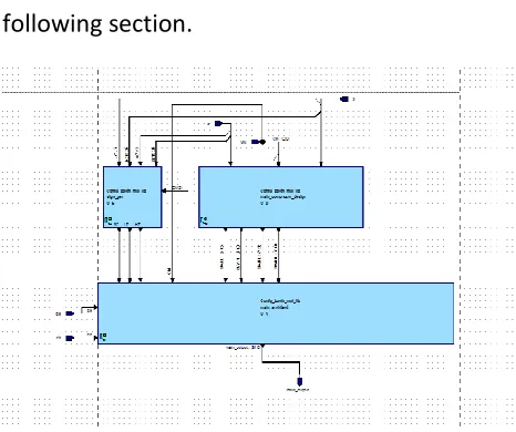
In this section, partially guarded
computation and the truncation technique are integrated into the configurable multiplication to construct a 16-b low-power CBM [11]. Figure 1 shows the block diagram of the proposed 16-b CBM. The configuration signals are utilized to configure the operation of the proposed multiplier into six modes as shown. When CM[2:1] = 11 or 10, the single 16-b or single 8-b multiplication operation is performed. On the other hand, two parallel 8-b multiplication operations that satisfy the high-throughput requirement are carried out if CM[2:1] = 00. The Bit CM[0] decides whether truncation has to be done or not, if it is 0 then truncation will be done through which more power saving and speed is obtained else the output product will not be truncated. Whenever truncation is done error compensation values will be added to maintain output
precision. The key components will be described and explained in detail in the following section.
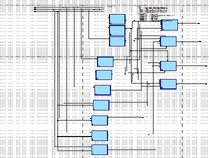
Fig 1 Dynamic Range Detector (DRD)
Given CM[2:0] and input operands A[15:0] and B[15:0] the proposed dynamic-range detector (DRD) in Figure 1 generates switching signals SWLH, SWHH, SWHL and SWLL for each 8-b Booth multiplication to pick the operand thatleads more partial products to zero for Booth encoding. In addition to switching signals, DRD produces several extra shutdown signals including SDLH, SDHH, SDHL, and SDLL to
dynamically disable the redundant
computation of the multiplier by forcing unnecessary partial-product bits and carry propagations to zero based on the multiplication mode and the effective range of the input operands.
Switching Logic:
3-bit group is successive zeros or ones so that its Booth encoded product will be zero. Finally each operand is compared to generate the switching signal that is used to determine which operand is a multiplier. In our design, the input operands will be exchanged if the switching signal is one. Aside from increasing the probability of Booth encoded products becoming zero, the switching logic can aid in detecting the length of the sign-extension bits of the input operands and shut down unnecessary computation.
Fig 2 Sign Bit Generator
If one of the input operands is zero, the entire operation of the configurable multiplier can be shut down to obtain more power savings by preventing input registers from loading new data and directly resetting the output registers to zero thereby increasing the speed of operation. Therefore, we develop an SBG as shown in Figure 4 to generate an SB, LZ and HZ and shut down the entire multiplier when one of the input operands is zero (clock gating technique [12] and [13]). In partially guarded computation, the
sign-extension bits of product are replaced by an SB to avoid unnecessary sign- extension computations.
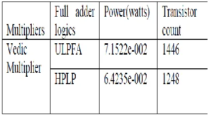
Vedic Multiplier
The design of the Vedic Multiplier led to a completely different aspect for the
established configurationally multiplier
which is designed for 2 bit, 4 bit serially and parallel. This additional feature has given an advantage for better signed and unsigned computations. It is proper to have only signed or unsigned hence we have modified the existing system to a even betterlow power and low area based system. Since we know that the Radix algorithm alone can solve both signed and unsigned but due design complexity factor and area factor we have reduce the design to 8 bit fully functional serial and parallel multiplier.
Logic for 2X2 Multiplication
MULTIPLIER(n=16) AREA (μm2) POWER (mW) DELAY (ns)
Radix2BoothMultiplier 2953 1.067 108.09
Radix4ModifiedBooth
Multiplier
3241 1.075 86.18
CBM[111] 3957 1.526 57.48
CBM[110] 2933 1.136 49.92
CBM[101] 873 0.323 30.16
CBM[100] 676 0.240 29.41
CBM[001] 1743 0.651 30.16
CBM[000] 1350 0.486 29.88
3. EXPERIMENTAL RESULTS:
For comparison, conventional Booth Multiplier using Radix 2 booth encoding and Radix 4 booth encoding for n=8 and n=16 and the proposed CBM for n=16 are designed in Verilog HDL and their simulation results were verified. These multipliers were synthesized by using the Synopsys Design Compiler with the TSMC 90nm CMOS standard cell technology
library. The implementation results,
including hardware area, critical path delay
and power consumption for these
multipliers, are given in Table II.
As can be seen, the area and delay of the proposed CBM very approximate to that of non configurable Radix 4 Booth Multiplier, although it is larger because additional circuits, including Shutdown logic, Switching Logic an SBG, an Error Correction Logic etc., are added to achieve configuration and for high speed operation.
Table IV. Comparison of Power for different data
When compared to Radix 4 Modified Booth Multiplier, the results in Table IV exhibit that CBM [111] is capable of achieving 52.05% power saving on average. Moreover, CBM [110] can further achieve 69.90% power saving on average by performing truncation and sacrificing a bit of output quality. On the other hand the speed of
operation also varies based on the input data. Consider the Table V which compares the critical path delay. CBM [111] is capable of achieving 57.32% increase in speed and CBM [110] can further achieve 65.62% increase in speed on average.
Table V. Comparison of Speed for different data
Vedic Multiplier:
4. CONCLUSION
A multi-functional configurable booth multiplier has been designed which provides a flexible arithmetic capacity and a tradeoff between output precision and
power consumption. Moreover, the
ineffective circuitry can be efficiently
deactivated, thereby reducing power
consumption and increasing speed of operation. The experimental results have shown that the proposed multiplier outperforms the conventional multiplier both Radix 2 Booth multiplier and Radix 4 Booth multiplier in terms of power and speed of operation. To avoid the expense of Area another Vedic multiplier circuit is
introduced for unsigned operations only which results in low power and low area.
REFERENCES:
[1] J.W Chen, R.H Yao, and W.J Wu, “Efficient 2n + 1 Modulo Multipliers,” IEEE Transactions on Very Large Scale Integration (VLSI) systems, V. 19, NO.12, 2011.
[2] Yuan-Ho Chen, Chung-Yi Li, and Tsin-Yuan Chang, IEEE, “Area-Effective and
Power-Efficient Fixed-Width Booth
[3] Valeria Garofalo, Nicola Petra and Ettore Napoli, “Analytical Calculation of the Maximum Error for a Family of Truncated Multipliers Providing Minimum Mean Square Error,” IEEE Transactions on Computers, V. 60, NO. 9, 2011.
[4] R. Nakamoto, S. Sakuraba, T. Onomi, S. Sato, and K. Nakajima, “4-bit SFQ Multiplier Based on Booth Encoder,” IEEE Transactions on Applied Superconductivity, V. 21, NO. 3, 2011.
[5] N. Petra, et.al “Design of Fixed-Width Multipliers With Linear Compensation Function,” IEEE Transactions on Circuits and Systems, V. 58, NO. 5, 2011.
[6] Ramya Muralidharan, and Chip-Hong Chang, “Radix-8 Booth Encoded Modulo 2n - 1 Multipliers With Adaptive Delay for High Dynamic Range Residue Number System,” IEEE Transactions on Circuits and Systems, V. 58, NO. 5, 2011.
[7] C.Y Li et.al, , “A Probabilistic Estimation Bias Circuit for Fixed-Width Booth Multiplier and Its DCT Applications,” IEEE Transactions on Circuits and Systems, V. 58, NO. 4, 2011.
[8] F. Lamberti, et.al “Reducing the Computation Time in (Short Bit-Width) Two’s Complement Multipliers,” IEEE Transactions on Computers, V. 60, NO. 2,2011.
[9] N. Petra, et.al “Truncated Binary Multipliers With Variable Correction and Minimum Mean Square Error,” IEEE
Transactions on Circuits and Systems, V.57, NO. 6, 2010.
[10] Shiann-Rong Kuang, and Jiun-Ping
Wang, “Design of Power-Efficient
Configurable Booth Multiplier,” IEEE
Transactions on Circuits and Systems, V. 57,NO. 3, 2010.
[11] A. Vazquez, E. Antelo, and P. Montuschi, “Improved Design of High-Performance Parallel Decimal Multipliers,” IEEE Transactions on Computers, V. 59,NO. 5, 2010.