c e-ISSN: 2348-6848, p- ISSN: 2348-795X Volume 2, Issue 12, December 2015
International Journal of Research (IJR)
Available at http://internationaljournalofresearch.orgOcNoC: Efficient One-cycle Router Implementation for
3D Mesh Network-on-Chip
L Pravallika Kammila
Mtech VLSIRamachandra College of Engineering
Dukkipati Venkanna Babu
Assst.ProfessorRamachandra College of Engineering
Abstract— Multiprocessor system on chip which is a most developed architecture with different features. One of the most important is networking. Networking which required high speed for the traffic permutation in which each input sends traffic to each output by using pipelined circuit switching network which is better compared with other on-chip network.
The pipelined circuit switching offers guarantee of permuted data with dynamic path setup scheme for selecting arbitrary schemes. Another most important aspect is Low Power Analysis which mainly reduced the leakage and optimists the dynamic power.
key words - Pipelined circuit switching; traffic permutation; dynamic path setup scheme; arbitrary scheme;
dynamic power consumption.
I.
INTRODUCTION
The multiprocessor System-on-Chip
(MPSoC) is a system-on-a-chip (SoC) which uses multiple processors usually targeted for embedded applications. It is used by platforms that contain multiple, usually heterogeneous, processing elements with specific functionalities reflecting the need of the expected application domain, a memory hierarchy and I/O components. All these Components are linked to each other by an on-chip interconnect. These architectures
meet the performance needs of multimedia applications, telecommunication architectures, network security and other application domains while limiting the power consumption through the use of specialized processing elements and architecture.
In switching technique the packet switching which required excessive amount of on-chip power and area for queuing buffer (FIFO) with per computed
queuing depth at the switching nodes and/or network interface so to avoid this we are using circuit switching with a dynamic path set up schemes. The dynamic path setup tackles the challenge of runtime path arrangement for conflict-free permuted data. The pre-configured data paths enable a throughput guarantee. By removing the excessive overhead of queuing buffers, a compact implementation is achieved and stacking multiple networks to support concurrent permutations in runtime is feasible.
II.
PROPOSED ON-CHIP
NETWORK DESIGN
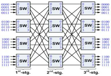
Network on-chip for which it required high speed for the traffic permutation where each input sends traffic exactly to each output for which we are using Clos network topology.
A. On-Chip Network Topology
c e-ISSN: 2348-6848, p- ISSN: 2348-795X Volume 2, Issue 12, December 2015
International Journal of Research (IJR)
Available at http://internationaljournalofresearch.orgmultiprocessors with thousands of nodes in macro systems.
Fig. 1. Proposed on-chip network topology with port addressing scheme.
Clos networks have three stages: the ingress stage, middle stage, and the egress stage. Each stage is made up of a number of crossbar switches often just called crossbars. Each call entering an ingress crossbar switch can be routed through any of the available middle stage crossbar switches, to the relevant egress crossbar switch. A middle stage crossbar is available for a particular new call if both the link connecting the ingress switch to the middle stage switch, and the link connecting the middle stage switch to the egress switch, is free.
The pipelined circuit switching is designed for the proposed network in which it first checks for status of a signal if the signal is ideal then its sends for the request once the signal is acknowledge of any available port then the circuit is acknowledge then transmit the signal for the output results and if the signal is blocked which means there is no available signals then its sends for back-tracking and it search again for two or more times for the signals if in case they are any available ports are there or not which sends nAck which means dead block.
Fig. 2. Switch-by-switch interconnection and path-diversity capacity
Fig. 3. Common switch architecture.
c e-ISSN: 2348-6848, p- ISSN: 2348-795X Volume 2, Issue 12, December 2015
International Journal of Research (IJR)
Available at http://internationaljournalofresearch.orgB. Dynamic Path Setup to Support Path Arrangement
A dynamic path-setup scheme is the key point of the proposed design to support a runtime path arrangement when the permutation is changed. Each path setup, which starts from an input to find a path leading to its corresponding output, is based on a dynamic probing mechanism. the operation of IC’s with its states to support backtracking probing operation. IC’s is triggered by the rising edge of the probing clock when processing an arriving probe header. Meanwhile, the ARBITER is triggered by the falling edge of the probing clock. The OC is simply implemented as a retiming stage for the control signals from the ARBITER and for handshake signals (i.e., Req and Ans) with the downstream switch. This implementation basis in the switch ensures that an arriving probe header is always processed in every probe cycle. For example, it is assumed that a probe header arrives at input 4. If there is no desired profitable outputs available, the IC’s will immediately (after one probing clock cycle) change from the Probing state into the Backtrack state to force the probe header to backtrack.
C. Back Track probing path-setup scheme
The path-setup scheme is essential and directly affects the overall performance of the circuit-switching approach. An analysis at the network-level, performed in previous work, confirmed the good performance of the backtracked routing circuit-switched NoC with the clos topology under certain communication patterns. In particular, in communications with larger packets, the data transmission duration can be long. This overwhelms the setup delay overhead, hence, improving the overall network performance.
D. Input Control
The IC is the key component to perform the backtracking probing task. This includes functions, such as processing history information of backtracking and dynamically constructing a table
of possible output ports for probing. when a request with the incoming probe header arrives, IC’s goes into the Probing state, compares the current switch address and the destination address to find possible outputs for probing.
Based on history information of backtracking, current availability of the output ports, and/or the feedback from the downstream switches, Ctrl In may change into the ACK, nACK or Backtrack states, correspondingly. These operations of Ctrl Ins consistently constitute the backtracking probing path-setup scheme supported by switches throughout each guaranteed throughput lane of the NoC. The CROSSBAR is designed as a cross-connection matrix implemented with output multiplexers in which each multiplexer is controlled by its corresponding OC’s. In combination with the internal transceivers, this cross-connection structure is capable of direct-forwarding a source-synchronous transmission of a clock along with data pipelined through the switch. The proposed switch architecture and its design can support the EPB-based probing path-setup scheme. It allows direct-forwarding of source-synchronous data.
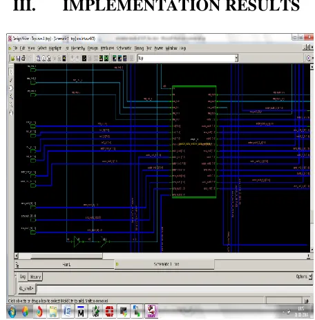
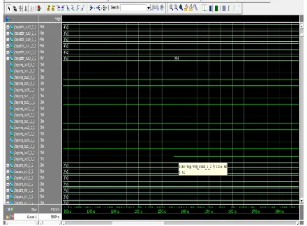
III. IMPLEMENTATION RESULTS
c e-ISSN: 2348-6848, p- ISSN: 2348-795X Volume 2, Issue 12, December 2015
International Journal of Research (IJR)
Available at http://internationaljournalofresearch.orgFig 6. Output Result
IV. LOW-POWER ANALYSIS
Low power has emerged as a principal theme in today’s electronics industry. The need for low power has caused a major paradigm shift where power dissipation has become as important a consideration as performance and area. In the past, the major concerns of the VLSI designer were area, performance, cost and reliability; power consideration was mostly of only secondary importance.
Power dissipation in CMOS circuits is caused by three sources: 1) the leak-age current which is primarily determined by the fabrication technology, consists of reverse bias current in the parasitic diodes formed between source and drain diffusions and the bulk region in a MOS transistor as well as the sub threshold current that arises from the inversion charge that exists at the gate voltages below the threshold voltage, 2) the short-circuit (rush-through) current which is due to the DC path between the supply rails during output transitions and 3) the charging and discharging of capacitive loads during logic changes.
The short circuit and leakage currents in CMOS circuits can be made small with proper circuit and device design techniques. The dominant
source of power dissipation is thus the charging and discharging of the node capacitances (also referred to as the dynamic power dissipation) and is given by:
P = 0.5CVd d2E sw fc l k
where C is the physical capacitance of the circuit, Vdd is the supply voltage, E(sw) (referred as the switching activity) is the average number of transitions in the cir-cuit per 1/fclk time, and fclk is
the clock frequency.
Low Power Analysis Output Results Measured at each Stages
Type of power
1st stage
2nd stage
3rd stage DRC(T=RC)
Static power
0.4484 mW
1.0201 mW
1.4685 mW
Dynamic power
0.9103 mW
1.8720 mW
2.7823 mW
Total power
1.4685 mW
2.7823 mW
4.2508 mW
DRC 3.7522
pSec
5.1427 pSec
4.6781 pSec
13.573 pSec
V.
CONCLUSION
c e-ISSN: 2348-6848, p- ISSN: 2348-795X Volume 2, Issue 12, December 2015
International Journal of Research (IJR)
Available at http://internationaljournalofresearch.orgA silicon-proven test-chip validates the proposed design and suggests availability for use as an on-chip infrastructure-IP supporting traffic permutation in future MPSoC researches.
VI. REFERENCES
[1]. Phi-Hung Pham, Junyoung Song, Jongsun
Park, and Chulwoo kim, Design and
Implementation of an On-Chip Permutation Network for Multiprocessor System-On-Chip, IEEE Transactions on Very Large Scale Integration (VLSI) systems, vol. 21, no. 1, January 2013.
[2]. Ahmed Jerraya, Wayne Wolf, Multiprocessor Systems-on-Chips, A volume in Systems on Silicon, Edition 2005.
[3]. M. Hubner and J.Becker (eds.), Multiprocessor System -on-Chip: Hardware Design and Tool Integration, Springer edition 2011.
[4]. By Sudeep Pasricha, Nikil Dutt, On-Chip Communication Architectures: System on Chip Interconnect, edition 2008. Multi-Stage Interconnection Networks.
[5]. P.-H. Pham, P. Mau, and C. Kim, ―A 64-PE folded-torus intra-chip communication fabric for guaranteed throughput in network-on-chip based applications,‖ in Proc. IEEE Custom Integr. Circuits Conf. (CICC), 2009, pp. 645–648.
[6]. http://www.ijser.org/paper/Low-Power-VLSI-High-End-Design-Techniques.html.
[7]. H. Moussa, O. Muller, A. Baghdadi, and M. Jezequel, ―Butterfly and Benes-based on-chip communication networks for multiprocessor turbo decoding,‖ in Proc. Design, Autom. Test in Euro. (DATE), 2007, pp. 654–659.