WHIRLCTRON- A Paramount Data Storage
Technology
Pooja Thakare, Pranav Kulkarni
Assistant Professor, Department of Electronics, KKWIEER, Nasik, India
TE Student, Department of Electronics, KKWIEER, Nasik, India
ABSTRACT: The spintronics is a field of research in physics and engineering. In this the electron is made to move in its orbit around the nucleus but in a specific direction. As a result of this we can differentiate between the binary data. So in this paper we will see the brief explanation of the working principle, then the advantages and applications of spintronics. It is related to the study intrinsic spin of electron and its associated magnetic field, in addition to its fundamental charge in solid state devices.
KEYWORDS : Spintronics, Magnetic Field, GMR.
I. INTRODUCTION
In the past few years there are many data storage technologies are came to known. Many of them are just came and gone but very few sustained because of their advantages,but still these technologies have many disadvantages like friction,mechanical vibrations,power losses,their size and other things. So to eliminate all these disadvantages there is “Spintronics” technology. It is based on the storage of data on the flux produced due to spinning of electron.
II. LITERATURE REVIEW
In 1900 Valdemar Poulsen demonstrated a telegrophone a device to record sound on to steel wire. After 35 years then in Berlin ,Fritz Pfleumer demonstrated a magnetophone, it is the first recording machine to use magnetic tape to preserve the voice. Then in 1952 IBM developed the 1st magnetic tape drive named as IBM 701 tape drive , it was able to record 700 characters per second with tape width of 13mm. The realization of semiconductors that are ferromagnetic above room temperature will potentially lead to a new generation of Spintronic devices with revolutionary electrical and optical properties. The field of Spintronics was born in the late 1980s with the discovery of the "giant magnetoresistance effect”. The giant magnetoresistance (GMR) effect occurs when a magnetic field is used to align the spin of electrons in the material, inducing a large change in the resistance of a material. A new generation of miniature electronic devices like computer chips, light emitting devices for displays, and sensors to detect radiation, air
pollutants, light and magnetic fields are possible with the new generation of Spintronic materials.
III. NEED OF SPINTRONICS
‘particles’ such as the electron. Electron spin is, after all, a quantum phenomenon. Many experts agree that Spintronics, combined with nanotechnology would offer the best possible solution to the problems associated with miniaturization mentioned above. Nano science and nanotechnology involve the study of extremely tiny devices and related phenomena on a spatial scale of less than one thousandth the diameter of a human hair or roughly half the diameter of
a DNA molecule.
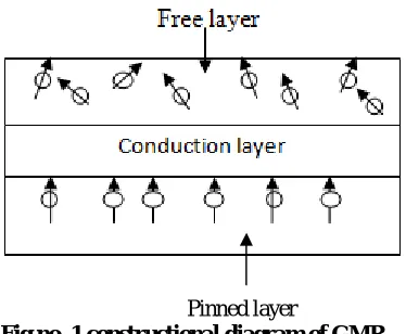
VI. GMR TECHNOLOGY
The GMR is an abbreviated for ‘Giant Magnetoresistance’. GMR is a very small magnetic effect found in thin layer of iron and other material. It is used to read and write information in hard drives. It is nanoscale technology but the change in resistance value is very drastic so it is called a giant magnetoresistance.
Pinned layer
Fig no. 1 constructional diagram of GMR
When direction of both the free layer electron & fixed layer electron will be same then the relative resistance of the GMR will be very low and there will be conduction of the current through conduction layer. But when the direction of electron is different in fixed layer and free layer then at this time there will be very high resistance offered by the GMR & hence there will be no conduction of current.
V. SPINTRONICS
The 1 TB of your hard disk drive can store up to 80 lakh songs. If you have seen the computers in 1980, there processor run at 8 MHZ clock frequency. Now a computer run at 4000 MHZ. So electronics produced amazing revolution. Spintronics is all about revolution of electron. As electronic devices become smaller, quantum properties of the wavelike nature of electrons are no longer negligible.
In the hard drive which is of very small size can store 1 TB of data, which is equal to 1,099,511,627,776 bits which is hardly countable. The thing is to store one bit of data we required the 1,099,511,627,776 bar magnets. Each of them is of size 30nm. And to read the data stored on each magnet the read-write head also need to be very small & it must have very good current diversity when it passes over the 1& 0 written over the Hard drive. And this can be achieved due to use of GMR. Now we have to reduce the size of hard disk & also its mechanical vibration as a result we have to reduce the number of bar magnets required. The electrons have physical property of “spin”. By using this property we can replace 1 bar magnet by just a 1 electron.
‘Consider simple example of sun and earth. When the earth is revolving around the sun it is also rotating around its axis. Same consider sun as nucleus & earth as an electron of an atom. When electron is moving around the nucleus it is rotating around its axis due to which a small amount of magnetic field is generated, and now this electron is treated as small bar magnet.’
Fig no. 3: Bar magnet and its magnetic field.
Fig no.4: Electron revolution creating magnetic field
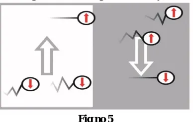
But the spin of electron is specially known as intrinsic angular movement. This spin of electron is given by ħ / 2. Now electronics is not only about the just flow of current but we have to control the flow of current.
As from the above figure we can see that when the direction of electron matches with the direction of polarization
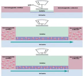
of material then there is smooth flow of electron through that material but when the direction of polarization of material is opposite to the direction of electron there is strong resistance to the flow of electron. On the same principle Datta-Das’s spin transistor was the first Spintronics device to be proposed for fabrication in metal oxide semiconductor.Datta-Das spin transistor was the first spintronic device to be proposed for fabrication in a metal-oxide-semiconductor geometry familiar in conventional microelectronics. An electrode made of a ferromagnetic material (purple) emits spin-aligned electrons (red spheres), which pass through a narrow channel (blue) controlled by the gate electrode (gold) and are collected by another ferromagnetic electrode (top). With the gate voltage off, the aligned spins pass through the channel and are collected at the other side (middle). With the gate voltage on, the field produces magnetic interaction that causes the spins to process, like spinning tops in a gravity field. If the spins are not aligned with the direction of magnetization of the collector, no current can pass. In this way, the emitter-collector current is modulated by the gate electrode.
Fig no. 6: Datta Das spin transistor
After the spin transistor proposed by Datta-Das another concept has been developed called all metal spin transistor by Mark Johnson at the Naval research Laboratory. The biggest disadvantage of all metal spin transistor is we cannot integrate it with existing semiconductor circuitry and the second disadvantage is that it cannot amplify the signal.
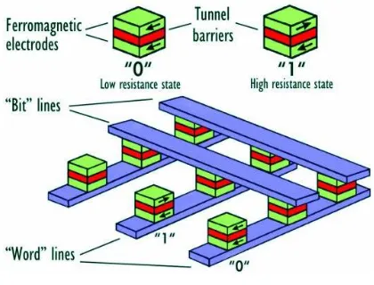
VI. MRAM
magnetic storage elements instead of electric used in conventional RAM .Tunnel junctions are used to read the information stored in Magnetoresistive Random Access Memory, typically a “0” for zero point magnetization state and “1” for antiparallel state.
Fig no. 7
VII. ELECTRONICS VS SPINTRONICS
Electronics Spintronics
Power failure problem No power failure problem
Based on properties of charge of the electron Based on intrinsic property spin of electron
Classical property Quantum property
Materials: conductors and semiconductors Materials: ferromagnetic materials
Based on the number of charges and their energy Two basic spin states: spin-up and spin-down
Speed is limited and power dissipation is high Based on direction of spin and spin coupling, high speed
VIII. ADVANTAGE
1. Low power consumption. 2. Less heat dissipation.
3. Spintronic memory is non-volatile.
4. Takes up lesser space on chip, thus more compact. 5. Spin manipulation is faster , so greater read & write speed.
IX. APPLICATION
1)Spintronics has several advantages over convintional electronics requres specialized semiconductor material in order to control the flow of charge through the transistor.
2)SPIN-FET – Spin polarized field effect transistor. In this device a non magnetic layer which is used for transmitting & controlling the spin polarized electron from source to drain. Here Spintronics plays an important role.
3) Information Storage Devices( Magnetic tape, Floppy Disk etc). 4) Micro electronic Devices.(MOSFET , BJT Etc.)
5) Sensors.(Measures the physical quantity and converts it into a signal which can be read by an instrument.)
X. CONCLUSION
This technology will exploit the spin of the electron and create new devices and circuits which could be more beneficial in future by providing devices like memories for data base accessing with the speed of light. The devices of this technology are very useful for transaction processing and for scientific number crunching.
Moreover, these "spintronic" devices might lead to quantum computers and quantum communication based on electronic solid-state devices, thus changing the perspective of information technology in the 21st century.
REFERENCES
1] Sankar Das Sarma, “A new class of device based on the quantum of electron spin, rather than on charge, may yield the next generation of microelectronics”, American Scientist, Volume 89. Published in2001 November–December.
[2] Das Sarma, S., et al. 2000. Theoretical perspectives on spintronics and spin-polarized transport. IEEE Transactions on Magnetics 36:2821. [3] Das Sarma, S., et al. 2001. Spin electronics and spin computation. Solid State Communications 119:207.
[4] Fabian, J., and S. Das Sarma. 1999. Spin relaxation of conduction electrons. Journal of Vacuum Science and Technology.