Concepts of Static Time Analysis in VLSI
Design
Kartik Jain1, Mimansa Maheshwari2
Under-Graduate Student, Dept. of ECE, L.D. College of Engineering, Ahmedabad, Gujarat, India1
Under-Graduate Student, Dept. of ECE, L.D. College of Engineering, Ahmedabad, Gujarat, India2
ABSTRACT: The main intention of this paper is to throw some light on Static Time Analysis(STA) and to present a lucid explanation of the parameters on which the timing analysis depends. As designs have grown in complexity, much effort has gone into initiatives focused on improving design efficiency and managing risk. What is not fully understood is the impact that timing constraints have on both. Poorly managed or incorrect analysis can have significant negative impact on design effort and can lead to a chip failure. The chances of this occurring are growing with every new technology nodes hence it is mandatory to have basic understanding in this field. This paper will help their readers to get a good idea on Timing concepts related to designing. The content of this paper is written after carrying out deep study of the books and related research papers.
KEYWORDS: Static Time Analysis, Setup Time, Hold Time, Metastability, Cross Talk
I. INTRODUCTION
We know that there is a step-wise procedure or a design-flow that is followed while synthesis of a digital device. This design flow begins with logic level designing followed by chip architecture (consists of power and timing related requirements), RTL level design using any hardware description language-its stimulation and verification through test vectors, synthesis of the RTL design, design for testability and to check if the design made meets the frequency requirements. Determining the maximum and minimum frequencies of input and clock required for the system for ensuring correct performance of design is also important. This method of checking the ability of the design to meet the intended timing requirements, statically without the need for simulation (no input is applied) is called static time analysis. If you look at the evolution of chip, timing plays an integral part at each step of the flow. It is constantly tweaked and verified as the design progresses through the implementation flow. This paper explains parameters affecting the analysis which are responsible for disturbing information transfer and incorrect latching of data resulting erroneous output. Information on parameters such as setup, hold, metastability and crosstalk are explained in detail and measures to prevent them are provided.
II. PARAMETERS OF STA
2) CLOCK LATENCY: The delay from the clock origin point to the clock definition point in the design is called Latency .It is the insertion delay external to the circuit which we are timing. It applies to only primary clocks.This delay is because of the capacitve load on the interconnect or elements in the clock tree between the clock source and the clock pin. Clock latency has two components – source and network latency.
Source latency is the delay from the source of the clock to the point where clock is defined. This source could be on-chip or off-on-chip.
Network latency is the time it takes for clock to propagate from the point where clock is defined to the point where it is actually used to trigger the sequential device.
There could be more than one clock path to a device, in which case the delays along the path could be different as well. The longest path or the one which has maximum delay is often referred to as the late path and shortest path or the one which has minimum delay is referred to as the early path . The total latency is the sum of source and network latency.
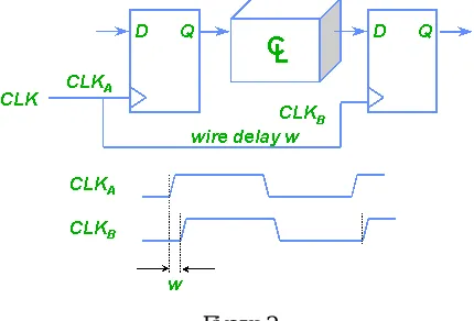
Figure 1
3) CLOCK SKEW: A phenomenon in synchronous circuits in which the clock signal arrives at different components at different times, due to wire-interconnect length, temperature variations, capacitive coupling, material imperfections and differences in input capacitance on the clock inputs.
There are two types of clock skew:
Negative skew: Occurs when the receiving register gets the clock tick earlier than the sending register.
Positive skew : Occurs when the transmitting register receives the clock tick earlier than the receiving register. Zero clock skew refers to the arrival of the clock tick simultaneously at transmitting and receiving register.
It is possible to reduce the clock skew by having a proper distribution of clock tree around the circuit. On such method is known as H-Tree distribution. The H-tree distribution is shown in the figure:
Figure 3 4) SETUP TIME :
Conventionally setup time is defined as minimum amount of time before the clocks active edge that the data must be stable for it to be latched correctly. To get basic understanding of setup time analysis we will consider two scenarios: one for ideal clock and then more practical scenario taking into consideration of real time clock.
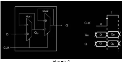
For Ideal clock : The clock is generated by an external phase locked loop circuit and it is considered to be ideal. To meet the timing condition i.e. data to be latched correctly, time taken by the data to reach capture flip-flop(ϴ), should be less than time period of the clock (t) i.e. ϴ < t. Looking toward more practical scenario and opening the capture flop we notice that it is made of many MOSFETs, resistors and capacitors. Representing capture flip-flop with the help of two multiplexers we get :
Figure 4
According to the figure at clock level zero output of mux1 (qm) becomes equal to input of the flip flop (d). Even multiplexers used to represent flip flop are made up of MOSFETS and other resistors and capacitors and so it takes some finite time to transfer information from input to output of MUX1(qm). This time required by flip-flop to settle the data in middle (at qm) is called Setup Time of the flip-flop represented by 's'. This time impacts the analysis and now for the output to be stable the time taken by data to reach capture flip-flop reduces as it requires some finite to settle data properly before the active edge and thus the equation changes to "ϴ < t - s"
One more practical scenario which affects the analysis is Skew resulting from addition of buffers to the clock tree. These buffers add delay on both data path and clock path. taking into consideration these delays the equation changes to
Figure 5
Left hand side of the equation is called "Data arriving time" and right hand side of the equation is known as "Data required time". For the information to be transferred correctly the difference between Data required time and Data arriving time should be positive. This difference is known as Slack and for data to latch properly slack should always be positive. For solving problems related to setup violations we can reduce data path delay, increase the size of cells or reduce the crosstalk impact on the nets.
5) HOLD TIME :
Definition:The amount of time the data at the synchronous input (D) must be stable after the active edge of clock is called hold time.
When we talked about setup time we considered the importance of the next coming input on the capture flip-flop and hence determined setup time based on the next clock edge that the capture flip flop was going to receive to produce output corresponding to the input given at the launch flip flop at the previous active clock edge. The concept of hold time is used to get the proper output at capture flip flop for the current edge present at the launch and capture flip flop. The image used below will be helpful in giving clear idea about the same.
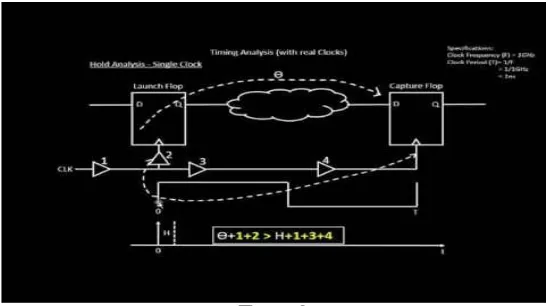
Figure 6
As shown in the figure ϴ indicates the total propagation delay that the signal takes in reaching at the input of the capture flip flop. There are buffers numbered 1, 2, 3 and 4 that are present at the clock line to solve problems related to clock jitters. We know that any flip flop element is made of a finite number of gate elements and each element posses a finite propagation delay hence for a particular received input there is a finite amount of delay after which the output is produced. Hence it is necessary to hold the present input in capture flip flop till the output is produced for the input. Let the time for which input should be maintained be H and hence " ϴ > H " should be a necessary this from that simple fact that the delay in arrival of the new input should be more so that the output from the previous input can be produced efficiently. Now consider the buffers used in clock line we need to consider delay of them as well. Hence the total propagation delay of the input arriving at capture flip flop becomes " ϴ+1+2 " and the delay for getting the output for the hold input in capture flip flop becomes " H+1+3+4 ".
Hence we get condition as shown in figure for the proper Output i.e.
Left hand side of the equation is called "Data arriving time" and right hand side of the equation is known as "Data required time". For the information to be transferred correctly the difference between Data arriving time and Data required time should be positive. This difference is known as Slack and for data to latch properly slack should always be positive. The problem of hold time violation can be solved by increasing data path delay, adding delay cell or creating detour for data path to increase net delay.
III.CONSEQUENCES OF VIOLATION OF PARAMETERS OF STA
METASTABILITY:
Whenever the change in data and clock is simultaneous or the order of change in data and clock is not proper then the problem of metastability arises. The digital device is said to be in metastable state when it has voltage level between state level for logic 0 and 1. Whenever any digital devices attains metastable state then it takes certain amount of time to settle to any one state. Moreover, the final logic is also not predictable.
Whenever any circuit takes more time than the total time from the instant the input is applied plus the propagation delay of the circuit to produce output it is said to be in metastable state. There are two important factors that determine metastability of circuit these factors are as follows:
1) Setup time 2) Hold time
The problem of metastability is not absolutely solvable however if there is a proper setup and hold time for the circuit then metastability can be reduced to a certain extent.
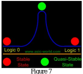
Figure 7
The relative stability of states shown in the figure above shows that the logic 0 and logic 1 states (being at the base of the hill) are much more stable than the somewhat stable state at the top of the hill. In theory, a flip-flop in this
stable hilltop state could remain there indefinitely but in reality it won't. Just as the slightest air current would eventually cause a ball on the illustrated hill to roll down one side or the other, thermal and induced noise will jostle the state of the flip-flop causing it to move from the quasi-stable state into either the logic 0 or logic 1 state.
MTBF is Mean time between failure, it gives us information on how often a particular element will fail or in other words, it gives the average time interval between two successive failures. The formula for calculating MTBF is mentioned below:
where
fCLOCK is the system clock frequency
fDATA is the data transfer frequency
tMET is the additional time allowed for the flip-flop to settle
C1and C2 are device specific parameters found by plotting the natural log of MTBF versus tMETand performing linear
regression analysis on the data
How to avoid Metastability?
Designers can tolerate metastability by making sure the clock period is long enough to allow for the resolution of quasi-stable states and for the delay of whatever logic may be in the path to the next flip-flop. This approach, while simple, is rarely practical given the performance requirements of most modern designs.
The most common way to tolerate metastability is to add one or more successive synchronizing flip-flops to the synchronizer. This approach allows for an entire clock period (except for the setup time of the second flip-flop) for metastable events in the first synchronizing flip-flop to resolve themselves. This does, however, increase the latency in the synchronous logic's observation of input changes.
Neither of these approaches can guarantee that metastability cannot pass through the synchronizer; they simply reduce the probability to practical levels.
IV. CROSSTALK
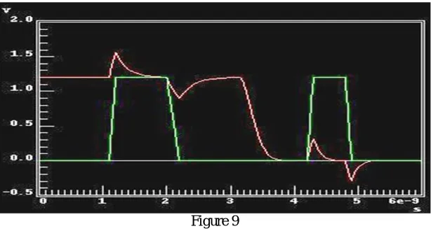
Crosstalk is the undesirable electrical interaction between two or more physically adjacent nets due to capacitive cross-coupling. The net that receives undesirable cross-coupling effects from a nearby net is known as "Victim" and the net that causes these effects in a victim net is called "Aggressor". Major factors which affects Crosstalk are distance between nets, length of nets, driver strength, timing window and slew rates. There are two major effects which affects the analysis:
1) Delay effect: This effect occurs when both the victim and aggressor nets exhibit a transition in same timing window and thus leads to either speed-up or slowdown of the signal on victim net resulting in timing violation.
Figure 8 2 ( ) 1 MET C t CLOCK DATA
e
MTBF
C
f
f
2) Noise effect: This takes place when aggressor net toggle causes glitch in the victim net. Unlike delay effect this effect is independent of the timing windows. This may lead to functional failures if these glitches are sufficiently large and get latched on a register.
Figure 9
Crosstalk can be prevented by increasing the spacing between the nets, shielding either the Aggressor or Victim net, increasing the width of nets, increasing the strength of driver on victim net, inserting buffer in problem net to reduce the net length.
V. RESULT AND DISCUSSION
Key factor in designing a correct circuit is proper clock distribution and proper analysis of clock behavior in the circuit. For this we carry out STA wherein a complete detailed study of clock behavior is performed for any designed circuit. The process of STA is needed to be performed several times during the designing and verification process. Even when there is any small change in the design it is necessary to carry out STA of the circuit again. There are tools like "Prime Time" by Synopsys, "SST" velocity by Mentor Graphics and "Celtic" by Cadence which are mainly used to perform STA. The main objective of the paper is to present a brief idea about STA and explain basic terminologies that are to be used in it. This paper intend to provide a good idea about STA to the beginners who are trying to learn STA in detail.
REFERENCES
[1] Ran Ginosar, “Metastabiltiy and synchronizers: A Tutorial,” IEEE design and Test in Computers.
[2] David Li, Pierce Chuang, Manoj Sachdev,” Comparative analysis and Study on Metastability of High performance Flip flops-Department of Electrical and Computer Engineering University of Waterloo, Waterloo, Ontario, Canada.
[3] Sridhar Gangadharan, Sanjay Churiwala, ”Constraining Design for Synthesis and Timing Analysis”.