Article
Optimization of MBE Growth Conditions of In
0.52Al
0.48As
Waveguide Layers for InGaAs/InAlAs/InP Quantum
Cascade Lasers
Piotr Gutowski, Iwona Sankowska, Tomasz Słupiński, Dorota Pierścińska, Kamil Pierściński, Aleksandr Kuźmicz, Krystyna Gołaszewska-Malec, Maciej Bugajski
1 Łukasiewicz Research Network-Institute of Electron Technology, Al. Lotników 32/46, 02-668 Warszawa, Poland;
[email protected] (P.G.); [email protected] (I.S.); [email protected] (T.S.);
[email protected] (D.P.); [email protected] (K.P.); [email protected] (A.K.); [email protected] (K.G-M.); [email protected] (M.B.)
* Correspondence: [email protected] (M.B.), Tel.: +48-22-5487-932
Abstract: We investigate molecular beam epitaxy growth conditions of micrometers-thick In0.52Al0.48As designed for waveguide of InGaAs/InAlAs/InP quantum cascade lasers. Effect of
growth temperature and V/III ratio on the surface morphology and defect structure were studied. The growth conditions which were developed for the growth of cascaded In0.53Ga0.47As/In0.52Al0.48As
active region, e.g. growth temperature of TG=520°C and V/III ratio of 12, turned out to be not
optimum for the growth of thick In0.52Al0.48As waveguide layers. It has been observed that after
exceeding ~1µm thickness the quality of In0.52Al0.48As layers deteriorates. The in-situ optical
reflectometry showed increasing surface roughness caused by defect forming, which was further confirmed by High Resolution X-Ray reciprocal space mapping, optical microscopy and atomic force microscopy. The presented optimization of growth conditions of In0.52Al0.48As waveguide layer
led to the growth of defect free material, with good optical quality. This has been achieved by
decreasing the growth temperature to TG=480 °C with appropriate increasing V/III ratio. At the same
time the growth conditions of the cascade active region of the laser were left unchanged. The lasers grown using new recipe have shown lower threshold currents and improved slope efficiency. We relate this performance improvement to reduction of the electron scattering on the interface roughness and decreased waveguide absorption losses.
Keywords: InAlAs; molecular beam epitaxy; surface morphology, quantum cascade lasers, X-ray spectroscopy
1. Introduction
Quantum cascade lasers (QCLs) emitting in the mid-infrared are in high demand for such applications as absorption spectroscopy in the molecular fingerprint region [1,2], free space
communication [3] and infrared countermeasures [4]. Mostly, they are designed using InGaAs/InAlAs material system epitaxially grown on InP single crystal substrates, as this group
offers wide possibilities of band-gap and wavefunction engineering with high values of band offsets [5]. They consist of the superlattice active region (AR), which is typically built of hundreds of thin
layers with thicknesses in the range of few nanometers, and the waveguide layers consisting of a few micrometers of bulk material, both grown in one epitaxial run. Technological feature often observed, is that the overall precision of layer thicknesses and their crystalline quality is very hard to achieve
at common growth conditions of these two main blocks of different character. In such case the main attention is put on strictly required AR superlattice periodicity and thickness control. Epitaxial
growth task in MBE is even more complex in case of strain-compensated QCLs, because such QCLs
demand a precise control of the composition of four ternary alloys, i.e. InGaAs and InAlAs in AR and
waveguide [6]. The optimum MBE growth conditions differ for thin (up to tens or low hundreds of nanometers) and micrometers-thick layers of ternary alloy. The former are the subjects of many
literature reports [7-11], as thin films of InGaAs and InAlAs material system on InP substrate are well developed for e.g. GHz-range transistors (HBT or HEMT) or telecommunication lasers, while the
thick, high crystalline quality InAlAs alloys required for QCL’s waveguides are rarely studied [12].
The MBE growth conditions which were developed for the growth of In0.53Ga0.47As/In0.52Al0.48As
active region superlattice of QCL, e.g. growth temperature of TG=520°C and V/III ratio of 12, turn out
to be not optimum for the growth of micrometers-thick In0.52Al0.48As waveguide layers. After
exceeding ~1 µm thickness the quality of In0.52Al0.48As layer deteriorates and formation of
microdefects e.g. Al- or In-enriched clusters or regions of ordered InAlAs alloy on the wafer surface
is observed. The in-situ optical reflectometry in MBE shows increasing surface roughness caused by
formed microdefects, which is further confirmed by optical microscopy, high resolution X-ray reciprocal space mapping and atomic force microscopy (AFM). We discuss results of diffuse X-ray
scattering in InAlAs alloy which shows different features of local chemical clusterring/ordering in crystalline InAlAs alloy depending on MBE growth conditions. AFM pictures show an increasing degree of atomic steps meandering at high thickness InAlAs. As the required waveguide thickness
in QCL is at least 2.5 µm, this local chemical clustering/ordering in InAlAs alloy, which can be controlled to some degree in MBE technology, significantly influences the device performance. In this
article, based on authors efforts to produce lattice matched In0.53Ga0.47As/In0.52Al0.48As/InP QCLs with
active region designed for emission wavelength of λ~9.2 µm, we present optimization of growth
conditions of In0.52Al0.48As waveguide layer leading to the growth of defect free material, with good
optical quality. A relatively narrow range of epitaxial conditions for the optimized growth of 2.5 µm
thick layers of In0.52Al0.48As alloy used as the main part of the QCL upper waveguide has been
determined.
The article is organized as follows: in section 2 the structures and experimental methods used
in the studies are described, in section 3 the experimental results of thick InAlAs layers growth versus epitaxial parameters are presented and discussed, including surface morphology studies by optical
microscopy, high resolution X-ray diffraction (HR XRD), atomic force microscopy (AFM) and photoluminescence (PL). Finally in section 4 the resulting QCL operation with optimized material of
thick InAlAs waveguide is presented.
2. Materials and Methods
For the purpose of this study, samples were grown in a Riber Compact 21T solid-source MBE, equipped with metal sources for In, Ga and Al, two cells of double-filament type for each metal, and As valved cracker source. MBE reactor was equipped with in-situ growth diagnostics tools, as pyrometry and optical reflectometry (Laytec) for beam wavelengths of 950 nm, 633 nm and 405 nm. For measurements of substrate temperature optical pyrometer (Modline) operating at the wavelength
940 nm was used. The pyrometer was calibrated at oxide desorption temperature from GaAs assumed here as 580°C, following values of 580-600°C originally given by Cho [7]. Standard
technique, using a beam flux monitor (BFM) located at the growth position was used for measurements of beam-equivalent pressure (BEP) of molecular fluxes, and reflection high energy
were calibrated based on high resolution X-ray diffraction measured for each QCL or test sample.
Beam flux monitor was used to control day-to-day stability of molecular sources, in particular to set the V/III ratio of arsenic to metal fluxes as one of the epitaxial growth parameters. It should be noted
that scaling of V/III ratio between different MBE machines may contain systematic uncertainties related to a particular construction and geometrical configuration of ion-gauge ensemble and may
produce different results in different MBE machines even by a factor of a few, e.g. based on our comparison of characteristic points on RHEED surface reconstruction maps for GaAs, which depend on both substrate temperature and V/III BEP ratio [13,14].
The QCL structures used in these studies are based on 4-well 2-phonon resonance AR design described in [15]. The waveguide from the bottom side was formed by a low doped InP substrate and
from the top by 2.5 μm AlInAs layer covered by heavily doped InGaAs layer. InAlAs waveguide material growth optimization was performed on dedicated test samples grown directly on InP
substrates to avoid the influence of another layer growth condition on investigated InAlAs. Besides saving the time and material, the more important is that using samples composed of mainly InAlAs
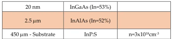
thick layer, the interpretation of InAlAs growth results is more direct than in the whole QCL structure. For that the simple test structure was drown up, like the one shown in Table 1.
Table 1. Schematic of test samples structure used to study In0.52Al0.48As growth optimization versus
two parameters in MBE: substrate temperature and V/III BEP ratio.
20 nm InGaAs (In=53%)
2.5 m InAlAs (In=52%)
450 m - Substrate InP:S n=3x1018cm-3
Series of test samples containing 2.5 μm thick layer of In0.52Al0.48As, were grown on InP (001)
substrates at temperatures in the 460°C -520°C range (as measured by pyrometry) and V/III ratio in
12-31 range. Growth rates ~0.8 μm/h were used for samples in reported studies. In0.52Al0.48As growth
was conducted in As-stabilized conditions (V/III ratio above 10) with surface reconstruction mostly
of (2x1) or (1x1) type as seen by RHEED. Sixteen samples were grown to establish the broad range of important technological parameters and make reliable comparison.
Samples were characterized using optical microscopy with Nomarski contrast to evaluate the
morphologyof the surface. High resolution X-ray diffraction (HR XRD) was used to measure lattice parameters and lattice mismatch to InP substrate, chemical composition of alloys, growth rates and
reciprocal space maps were recorded to check for a lack of elastic relaxation of layers and to evaluate intensity of diffuse X-ray scattering. Cu Kα1, = 0.1502 nm radiation was used in triple crystal
diffraction geometry [16]. All samples were studied by photoluminescence (PL). The PL spectra were collected by a Nicolet-8700 Fourier Transform Infrared (FTIR) spectrometer. For the PL studies
samples were mounted on the cold finger of the LHe continous flow cryostat and optically pumped with a 650 nm (1.91 eV) laser diode. The PL was collected with off-axis parabolic metal mirror. The experiment was performed in the step-scan (double modulation) mode. The excitation laser was
pulse operated (pulse width of 1.15 ms), with trigger signal referencing the lock-in amplifier. Atomic force microscopy (AFM) was used to evaluate growth features of the surface.
3.1. Background of the problem
In this part, experimental results on optimization of growth conditions of micrometer-thick In0.52Al0.48As waveguide layers for InGaAs/InAlAs/InP QCLs will be presented. Considering the
standard growth conditions which were developed for growth of AR [6], e.g. growth temperature of
TG=520 °C and V/III ratio of 12, such layer could be grown with high morphological perfection up to
about 1 μm thickness, as recognized from our study of the growth of different thickness test samples.
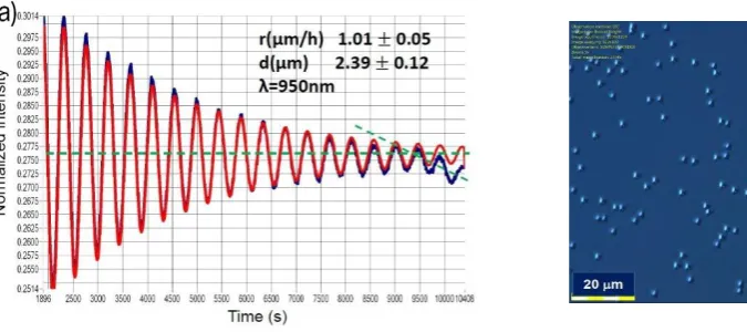
After exceeding that thickness the formation of microdefects (i.e. micrometer size defects) on the wafer surface was observed (c.f. Figure 1).
Figure. 1. (a)Comparison of normalized intensity of optical reflection at wavelength 950 nm from the
surface of In0.52Al0.48As sample measured during MBE growth for microdefects-free growth (red line)
and for growth with the onset of microdefects and related roughening of sample’s surface in microscale
(blue line). Reflectivity was recorded for growth of 2.5 µm thick In0.52Al0.48As layer of upper waveguide
on top of QCL active region. Growth rate was ~1 μm/h. (b) Nomarski microscopy picture of surface of
2.5 μm thick In0.52Al0.48As layer for sample with microdefects developed during MBE growth.
The MBE in-situ optical reflectometry showed increasing of surface roughness manifesting itself
as a decrease of average optical reflection signal at growth time around t=9500 sec (c.f. Figure 1a - blue line) in comparison to microdefects-free growth (red line). Microdefects were clearly seen on sample surface in Nomarski microscopy, Figure 1b. It was also noted that the presence of
microdefects significantly influenced the QCL device performance by a decrease of optical quality of the waveguide material and increased optical losses. Such microdefects can also decrease the
breakdown voltage of dielectric layer deposited during the processing technology of QCL device. These two reasons have significant influence on limiting the laser performance as well as the device
reliability and yield.
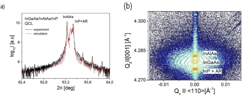
X-ray diffraction profile presented in Figure 2a was used to measure mismatch of layers to InP
substrate and the periodicity of AR superlattice structure. Reciprocal space map of X-ray intensity presented in Figure 2b shows a significant diffuse scattering close to 004 Bragg reflection. It is seen as a spreading of intensity contour lines close to the 004 reciprocal lattice point. It can be seen that the
diffuse scattering is located mainly around InAlAs thick layer’s peak position. So, this diffuse scattering is related to microdefects in InAlAs thick layer. Presence of such diffuse X-ray scattering
microdefects. Test QCL structures prepared with ~1 m thick InAlAs waveguide layer showed no
X-ray diffuse scattering in reciprocal space maps.
Figure. 2. (a) ω/2θ scan of QCL sample. (b) Reciprocal space map of X-ray intensity around 004 Bragg
reflection for QCL sample. Diffuse X-ray scattering is seen as isointensity contours growing in
horizontal direction, i.e. perpendicular to [004] Bragg diffraction vector which is displayed in vertical
direction on the map. Subsequent contours of X-ray intensity are shown in logarithmic scale and
separated by a factor of ~3.
Such microdefects in InAlAs grown close to the lattice-matched condition on InP have origin from the presence of aluminum, as they are created only during the growth of InAlAs, but not for
InGaAs, even up to 3 µm thickness tested by us. It will be shown below that by a careful optimization of growth conditions, e.g. growth temperature and V/III ratio, there is a possibility to minimize their
density on the surface, or remove almost all growth-related microdefects. Some random origin microdefects, e.g. the oval defects connected with MBE technology, are still present, but their number
is rather small and seems to be independent on MBE growth conditions.
Microdefects in InAlAs/InP described in the literature were reported to depend strongly on the growth conditions, with a rather narrow range of technological parameters of microdefects-free
growth [9,12,17] around 500 °C, also with improved InAlAs properties at much higher temperatures around 600 °C [18] or around 650-750°C used in MOVPE [19]. It is however, difficult to accurately
compare various defects reported in relation to growth conditions due to different temperature calibrations used in different growth methods or by different research groups. Our purpose here is
to describe defects met in authors efforts of developing the technology of microdefects-free thick In0.52Al0.48As epitaxial layers and relate the microdefects observed to literature reports, based mainly
on X-ray scattering studies.
Growth conditions optimization was performed in function of two main epitaxial parameters
which are well controlled in MBE; the substrate temperature and the V/III ratio, for a fixed growth rate 0.8 μm for all samples studied. Four different substrate temperatures for growth of test structures
were chosen; Tg= 520°C, 500°C, 480°C and 460°C. At each growth temperature the V/III ratios tested:
were 12, 17, 26 and 31. Sixteen samples were grown to establish the broad range of important technological parameters and make reliable comparison. All test samples were designed to have
InAlAs composition shifted toward slightly higher AlAs composition than In0.523Al0.477As alloy lattice
3
10
− ⊥
. Lattice mismatch was defined, as ( ) ( )( )
a InAlAs a InP
a InP
⊥
⊥
−
= , where a InAlAs⊥( )is lattice
parameter of fully strained (in these studies) InAlAs layer in direction perpendicular to InP (001) surface, and
a InP
(
)
is lattice parameter of InP substrate. It has been achieved by careful control oflattice mismatch in MBE growth using HR XRD.
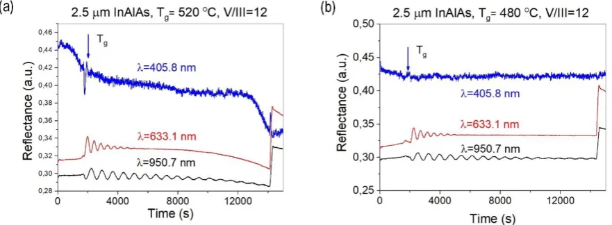
During the growth of test structures, the optical reflectometry signal was collected in real time, similarly as described above for QCL growth. Figure 3 shows the comparison of optical reflectance for three different wavelengths; 405.8 nm, 633.1 nm and 950.7 nm, recorded at two substrate
temperatures; 520°C and 480°C. In the latter case, the substrate temperature was first raised to 520°C, and then ramped down to 480°C to start the growth process.
Figure 3.Optical reflectance signals recorded during growth of 2.5 μm thick In0.52Al0.48As layers: (a)
Tg = 520°C, V/III = 12 and (b) 480°C, V/III = 12.
For all wavelengths the drop of reflectance with time was observed. For quantitative estimation of this effect we have compared the relative decrease of reflectance at probe wavelength of 633.1 nm at the end of the growth process for all growth conditions investigated. The results are summarized
in Table 3. The decrease of reflectance for growth temperature Tg=480°C is noticeable smaller than for any other substrate temperature. The observed signal drop is related to an increase of surface
roughness, due to forming of microdefects visible on the sample surface and is in a good correspondence to optical microscopy observations and XRD results, as it will be shown below.
However, even for samples showing a significant drop of reflectivity, the surface roughening does
not develop at the layer thickness less than ~1 μm, indicating some accumulative mechanism of the
onset of microdefects formation.
Table 2. The relative decrease of reflectance at probe wavelength of 633.1 nm at the end of the growth process of 2.5-m InAlAs layer for all investigated substrate temperatures and V/III ratios.
V/III=31 V/III=26 V/III=17 V/III=12
520 °C -8,90% -5,45% -6,04% -8,11%
500 °C -1,94% -3,59% -2,84% -2,43%
480 °C -0,51% -0,15% -0,12% -0,03%
3.2. Surface morphology
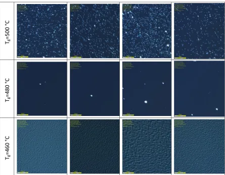
Test samples were inspected after the growth process by optical microscope in order to compare
surface morphology. The results are presented in Figure 4. Comparing pictures in the columns of constant V/III ratio, a strong dependence is observed between in the surface density of growth-related
morphological microdefects versus growth temperature. At the same time, comparing pictures in each row, much weaker dependence of microdefects density on V/III ratio is seen. The highest surface
densities of growth-conditions-dependent microdefects and the largest their size, visible in Nomarski contrast, are present in structures grown at 520°C. Similar temperatures are used as a standard
growth conditions for this material in many reports, e.g. [9,10,12], however usually for thickness well
below 1 μm. The reduction of growth temperature to 500 °C (second row in Fig. 4.) leads to a small
decrease of visible microdefects density and size. An almost clean surface is visible for growth
temperature in a narrow range arround Tg = 480 °C (third row in Figure 4). Further temperature
reduction to 460°C leads to a 3-dimensional (3D) growth with a dense micro-roughness morphology
of different type than isolated microdefects seen for temperatures 500 °C and 520 °C.
This comparison clearly shows the dominating role of substrate temperature for the
development of morphological features in micrometer-scale (microdefects), with only weak dependence on V/III ratio. Also, a very different morphologies are seen for both the two highest
temperatures and for the lowest temperature. At high temperatures 520 °C and 500 °C isolated microdefects distributed on the crystal surface in a close to random manner are seen, while for the
lowest temperature 460 °C a dense or continuous micro-roughness is present, with a weak directional texture visible. From material optimization point of view, it is seen that in between growth temperature regions of two different types of microdefects, there is a rather narrow window of
optimized substrate temperature around 480 °C, probably not wider than ~20-30 °C, which allows for almost microdefects-free growth of high structural and presumably high optical quality InAlAs
alloy thick layers, appropriate for the waveguide of QCL. This low concentration of microdefects seen for samples grown at 480 °C is almost independent on the V/III ratio in the range studied. It is seen
that the surface temperature during growth plays a more basic role than V/III ratio (in As-rich conditions used) in controlling of the surface morphology. In the next section, devoted to X-ray
studies, we will provide more specific discussion on the crystalline features behind these morphologies.
V/III=31
V/III=26
V/III=17
V/III=12
T
g=5
20
T
g=5
00
°C
T
g=4
80
°C
T
g=4
60
°C
Figure 4. Matrix of optical microscopy pictures (Nomarski contrast) of 0.1x0.1 mm2 surface area of 2.5 m thick InAlAs/InP test samples shown versus MBE growth parameters, where rows are for constant substrate temperature and columns are for constant V/III ratio.
To learn more about the mechanisms of nucleation of microdefects we have performed AFM studies for selected samples. Figure 5 shows AFM results of surface structure of sample at optimal growth conditions (Tg = 480°C, V/III ratio =26). Atomic steps visible on the surface of thick InAlAs layer shows distinct meandering, which is characteristic for growth at low temperature and low surface mobility of adatoms. From the meanders size of ~100 nm one may expect that the diffusion lengths of adatoms on the surface is not larger than dozens of nanometers. In spite of such meandered structure of atomic steps the sample in Figure. 4 for conditions Tg = 480°C, V/III ratio =26 shows very
small surface density of microdefects. For samples grown at higher or lower temperatures than the
optimum Tg = 480°C AFM pictures did not show resolved atomic steps which might be consistent
Figure 5.AFM pictures of surface structure of InAlAs 2.5μm thick layer grown on InP (001) substrate at optimal conditions Tg = 480°C, V/III ratio =26. Right panel shows an enlarged scale. High meandering of atomic steps for growth at this relatively low temperature is visible in spite of low surface density of microdefects developed at such growth conditions as shown in Figure 4.
3.3 Structural characterization
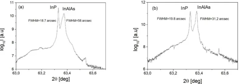
High resolution X-ray diffraction (HR XRD) was used as a standard characterization technique for all samples, to measure the composition of InAlAs alloy, lattice mismatch to InP substrate and layer thickness, while reciprocal space maps were used to evaluate the presence of local lattice distortions and structural fluctuations due to microdefects. Figure 6 shows /2 scans of InAlAs test samples for growth temperatures Tg = 520 °C and Tg = 480°C and V/III = 17.
Figure 6. The /2scans of InAlAs/InP test samples for growth temperatures: (a) Tg = 520 °C and (b) T=480°C. V/III = 17 flux ratio was used in both cases.
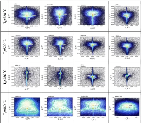
Figure 7. Reciprocal space maps of XRD intensity (contour plots) measured around 004 symmetrical reflection of InAlAs/InP test samples for growth temperatures: (a) Tg = 520 °C and (b) Tg = 480°C. V/III = 26 flux ratio was used in both cases.
Reciprocal space maps of XRD intensity measured around 004 symmetrical reflection for InAlAs/InP test samples are shown in Figure 8.
T
g=5
20
°C
T
g=5
00
°C
T
g=4
80
°C
T
g=4
60
°C
Figure 8. Reciprocal space maps of XRD intensity (contour plots) measured around 004 symmetrical reflection for InAlAs/InP test samples shown versus MBE growth parameters, where rows are for constant substrate temperature and columns are for constant V/III ratio. In the intensity direction, z-axis, the contours are drawn equally spaced in logarithmic scale from the Bragg maxima (~106 cps, counts per second in diffractometer units, to 1 cps background); close contours differ in intensity by a factor of 4. Coordinates of 004 Bragg reflection for InP are approximately (Qx, Qz) = (0, 4.28) Å-1, Qx // [110] and Qz // [001] are reciprocal space vectors, in all panels. Units of scales in Qz directions differ in various panels.
At close-to-optimal temperature 480 °C (see Figure 4) a high crystalline perfection of InAlAs layer is seen for V/III ratio not higher than 17, where the diffuse X-ray scattering (DXS) intensity is very low. At higher and lower temperatures, a significant portion of diffusely scattered X-ray intensity around Bragg 004 reflection is visible as widely spread intensity contours. It is seen that the symmetry features of DXS contours in the reciprocal space maps are different for the case of isolated microdefects (520°C and 500°C as in Figure 4), where DXS has more isotropic character, and at low temperature (460°C) where DXS contours elongated in reciprocal space in approximately <111> type directions indicate anisotropic features of microdefects. Distinct anisotropic features are also visible for 480 °C at low V/III ratio = 12, 17, although at low DXS intensity.
Distinct structural features of In0.52Al0.48As test samples can be seen in X-ray reciprocal space
samples grown at substrate temperature 480°C showing low surface density of morphological microdefects, X-ray intensity maps shows a narrow distribution concentrated in 004 Bragg reflection maxima for InAlAs layer and InP(001) substrate, as seen in Figure. 8 for the row at 480°C and for high V/III ratio of 26 and 31. While for samples with a high density of surface microdefects, that is going to higher 500-520°C or lower 460°C temperatures in Figure 4, a much wider distribution of X-ray intensity scattered around 004 Bragg maximum is visible in respective panels in Figure 8. Such X-ray intensity widely diffusely distributed around reciprocal lattice points (known as diffuse X-ray scattering, DXS) originates from weak deviations of crystal structure from the ideal periodicity [20-23], or in other words from the structural disorder in crystals or crystalline alloys, and is related to a presence of various structural defects [22] of crystal structure or structural fluctuations in a crystalline alloy [23] (Sections 1.5, 3.2). In Figure 8, DXS is visible as a spreading of intensity contours around 004 Bragg reflection. Summing this up, in Figure 8 going from 480°C to either higher or lower temperatures a significant increase of DXS intensity is seen, which is in a good correspondence with an increase of surface density of microdefects in Figure 4.
3.4. Photoluminescence
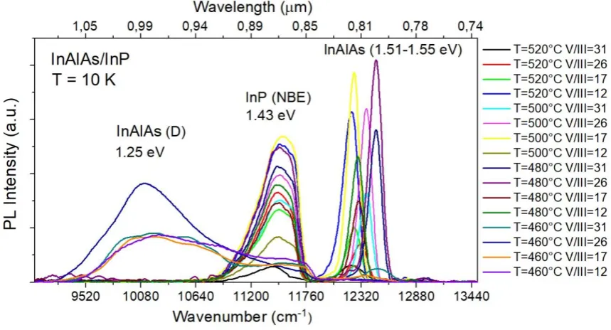
Photoluminescence spectra of all samples investigated are plotted in Figure 9. For the PL studies samples were mounted on the cold finger of the LHe continous flow cryostat and optically pumped with a 650 nm (1.91 eV) laser diode.
Figure 9. Low temperature PL spectra of InAlAs/InP samples grown in different temperatures and V/III flux ratios. PL was excited by 650 nm (1.91 eV) laser diode.
Three groups of transitions are present in the low-temperature spectra. The lines peaked at ~1.51 eV-1.55 eV can be attributed to near band edge (NBE) luminescence of the InAlAs layer [24,25].
Energy spread of their positions results from differences in alloy’s composition, which were indeed
confirmed by X-ray diffraction. The second group of lines, peaked at 1.43 eV is the near band edge (NBE) luminescence of InP substrate [26]. Both the position and the halfwidth (~50 meV) of these lines
correspond well with doping of the substrate (3x1018cm-3). Weaker long-wavelength band D is also
seen around 1.25 eV. It is observed only in material grown at 460oC be attributed to defect related
emission in InAlAs. Its appearance is accompanied by quenching NBE luminescence. D band is
absent in the material grown at optimum growth temperature of 480oC but is also not seen in high
confirmed by X-ray studies. That means that nature of the defects generated in both temperature ranges, below and above optimum growth temperature window is different.
The full width at the half maximum (FWHM) of the near band edge InAlAs PL signal was measured. The results are summarized in Table 3. It shows that for temperatures close to optimum growth window, as determined from X-ray studies, the NBE peaks are narrowest, which might be directly related to their crystalline quality.
Table 3. The FWHM of the near band edge InAlAs PL signal for 2.5-m InAlAs layer for all
investigated substrate temperatures and V/III ratios.
FWHM V/III=31 V/III=26 V/III=17 V/III=12
520 °C 19.0 nm 12.3 nm 10.9 nm 12.6 nm
500 °C 9,5 nm 9.8 nm 9.8 nm 9.9 nm
480 °C 9.3 nm 9.8 nm 9.8 nm 9.9 nm
460 °C 19.3 nm 42.7 nm 23.6 nm 52.0 nm
Experiments based on carrier transport indicate that the InAlAs alloy grown by MBE may exhibit significant clustering. Clustering generally has a detrimental effect on the optical and transport properties of materials [11]. Due to the large difference between In-and AI-related bond energies the
Ino.52 AloA8 As system is expected to show clustering due to the low temperatures employed in MBE
growth [27-30].
3.5. Device results
The QCL structures were grown using lattice-matched In0.53Ga0.47As/In 0.52Al0.48As active region.
of 4-well 2-phonon resonance design [15]. The layer sequence of one period of the structure, in nanometers, starting from the injection barrier was: 4.0, 1.9, 0.7, 5.8, 0.9, 5.7, 0.9, 5.0, 2.2, 3.4, 1.4, 3.3,
1.3, 3.2, 1.5, 3.1, 1.9, 3.0, 2.3, 2.9, 2.5, 2.9 nm. The waveguide from the bottom side was formed by a
low doped InP substrate and from the top by 2.5 μm AlInAs layer covered by heavily doped InGaAs
layer. The details of the layer structure of grown devices are listed in the Table 4.
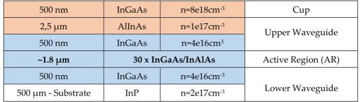
Table 4. Layer structure of In0.53Ga0.47As/In0.52Al0.48As/InP laser.
500 nm InGaAs n=8e18cm-3 Cup
2,5 µm AlInAs n=1e17cm-3
Upper Waveguide
500 nm InGaAs n=4e16cm3
~1.8 μm 30 x InGaAs/InAlAs Active Region (AR)
500 nm InGaAs n=4e16cm-3
Lower Waveguide 500 µm - Substrate InP n=2e17cm-3
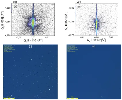
Figure 10. Reciprocal space map of X-ray intensity around 004 Bragg reflection for QCL sample grown at constant temperature Tg=520°C and V/III=12 (a) and at the optimized growth technology (b). Surface morphology for sample grown at constant temperature Tg=520°C and V/III=12 (c) and at the optimized growth technology (d).
The grown structures were processed into double trench Fabry-Perot lasers using standard
processing technology [31]. For isolation layer Si3N4 was used. Low resistivity electrical contacts were
alloyed at 370 °C for 60 s. Ti/Pt/Au alloy was used to the epi-side, and AuGe/Ni/Au for low doped substrate side. The lasers were cleaved into bars with length of 2 mm and mounted epi-side up on
Au-plated AlN submount. Figure 11 shows comparison of the room temperature electro-optical
characteristics of the laser grown according to optimized growth technology and the one grown at
constant temperature Tg=520°C and V/III=12. QCL grown at optimized conditions exhibits threshold
current density of 6.67 kA/cm2, comparing to 7.53 kA/cm2 for laser grown at constant temperature
Figure 11 The room temperature electro-optical characteristics of two lasers; the one grown according to optimized growth technology and one grown at constant temperature Tg=520°C and V/III=12.
4. Conclusions
We have investigated molecular beam epitaxy growth conditions of micrometers-thick
In0.52Al0.48As designed for waveguide of InGaAs/InAlAs/InP quantum cascade lasers. Effect of growth
temperature and V/III ratio on the surface morphology and defect structure were studied. The presented optimization of growth conditions of In0.52Al0.48As waveguide layer, based on the extensive
X-ray diffraction studies, optical microscopy, AFM and photoluminescence, led to the growth of defect free material, with good optical quality. This has been achieved by decreasing the growth
temperature of the InAlAs waveguide to TG=480 °C and increase of V/III ratio to 26. At the same time
the growth conditions of the cascade active region of the laser were left unchanged comparing to our
previous work; i.e. they stayed at TG=520 °C and V/III ratio equal to 12. The lasers grown using new
recipe have shown lower threshold currents and substantially improved slope efficiency. We relate this performance improvement to reduction of the electron scattering on the interface roughness and decreased waveguide absorption losses.
Author Contributions: MBE growth, P.G. and T.S.; X-ray characterization, I.S., AFM characterization, K.G-M.; device fabrication, A.K.; device characterization, K.P. and D.P.; writing, M.B., P.G and T.S.; methodology, D.P.; supervision, review and editing, M.B. All authors discussed results and contributed to formulation of conclusions.
Funding: This research was funded by National Center for Research and Development (Poland), project Techmatstrateg SENSE no. 1/347510/15/NCBR/2018 and National Science Center (Poland), projects no. 2015/17/B/ST7/04015 (OPUS 9).
Conflicts of Interest: The authors declare no conflict of interest.
References
1. Zhenhui Du, Shuai Zhang, Jinyi Li, Nan Gao, Kebin Tong. Mid-Infrared Tunable Laser-Based
Broadband Fingerprint Absorption Spectroscopy for Trace Gas Sensing: A Review. Appl Sci.2019, 9, 338;
doi:10.3390/app9020338
2. Curl, F.; Capasso, F.; C. Gmachl, C.; Kosterev, A.A; McManus, B.; Lewicki, R.; Pusharsky, M.; Wysocki,
G.; Tittel, F.K. Quantum cascade lasers in chemical physics. Chem. Phys. Lett. 2010, 487, pp. 1-18
3. Mikołajczyk, J.; Bielecki, Z., Bugajski, M.; Piotrowski, J.; Wojtas, J.; Gawron, W.; Szabra, D.; Prokopiuk, A.
Analysis of free space optics development, Metrol. Meas. Syst. 2017, 24, pp. 33–38;
DOI: 10.1515/mms-2017-0060
4. Maulini, A.; Lyakh, A.G. Tsekoun,; Go, R.; Lane, M.; Macdonald, T.; Kumar, C.; Patel, N. High power,
high efficiency quantum cascade laser systems for directional infrared countermeasures and other
defense and security applications. 2009, SPIE Proceedings Volume 7483, Technologies for Optical
Countermeasures VI; 74830D; https://doi.org/10.1117/12.830228
5. Faist, J. Quantum Cascade Lasers, Oxford University Press, Oxford, 2013
6. Gutowski, P.; Sankowska, I.; Karbownik, P.; Pierścińska, D.; Serebrennikova, O.; Morawiec, M.;
Pruszyńska-Karbownik, E.; Gołaszewska-Malec, K.; Pierściński, K.; Muszalski, J.; Bugajski, M. MBE
growth of strain-compensated InGaAs/InAlAs/InP quantum cascade lasers. Journal of Crystal Growth2017,
466, pp. 22-29 http://dx.doi.org/10.1016/j.jcrysgro.2017.02.031
7. Cho, A.Y. Growth of III-V semiconductors by molecular beam epitaxy and their properties.Thin Solid
Films1983, 100, 291 https://doi.org/10.1016/0040-6090(83)90154-2
8. Cheng, K.Y.; Cho, A.Y.; Wagner, W.R.; Bonner, W.A. Molecular beam epitaxial growth of uniform
In0.53Ga0.47As on InP with a coaxial In‐Ga oven. J. Appl. Phys.1981, 52, 1015
https://doi.org/10.1063/1.328798
9. Georgakilas A.; Halkias, G.; Christou, A.; Kornilios, N.; Papavassiliou, C.; Zekentes, K.; Konstantinidis,
G.; Peiró, F.; Cornet, A.; Ababou, S.; Tabata, A.; Guillot, G. A Comprehensive Optimization of InAlAs
Molecular Beam Epitaxy for InGaAs/InAlAs HEMT Technology. J.Electrochem. Soc.1993, 140, 1503
https://doi.org/10.1149/1.2221587
10. Choi, W-Y.; Fonstad, C.G. Growth optimization of molecular beam epitaxy grown InAlAs on InP. J. Vac.
Sci. Technol.B 1994, 12, 1013 https://doi.org/10.1116/1.587117
11. Praseuth, J.P.; Goldstein, L.; Hénoc, P. Primot, J. Investigation of crystalline and optical properties of
Al0.48In0.52As grown by molecular‐beam expitaxy.J. Appl. Phys.1987, 61, pp. 215-219
https://doi.org/10.1063/1.338859
12. Lee, W.; Fonstad, C.G. The growth of high mobility InGaAs and InAlAs layers by molecular beam
epitaxy. J. Vac. Sci. Technol. B1986, 4, pp. 536-538 https://doi.org/10.1116/1.583421
13. Daweritz, L.; Hey, R. Reconstruction and defect structure of vicinal GaAs(001) and AlxGa1−xAs(001)
surfaces during MBE growth. Surf. Sci.1990, 236, pp. 15-22 https://doi.org/10.1016/0039-6028(90)90756-X
14. Regiński, K.; Muszalski, J.; Preobrazhenskii, V.V.; Lubyshev, D.I. Static phase diagrams of reconstructions
for MBE-grown GaAs(001) and AlAs(001) surfaces. Thin Solid Films 1995,267, pp. 54-57
doi:10.1016/0040-6090(95)06665-9
15. Gutowski, P.; Karbownik, P.; Trajnerowicz, A.; Pierściński, K.; Pierścińska, D.; Sankowska, I.; Kubacka
-Traczyk, J.; Sakowicz, M.; Bugajski, M. Room temperaturę AlInAs/InGaAs/InP quantum cascade lasers.
Photon. Lett. Poland2014, 6, pp. 142-144 doi: 10.4302/plp.2014.4.10
16. Kubacka-Traczyk, J.; Sankowska. I.; Seeck O.H.; Kosiel, K.; Bugajski M. High-resolution x-ray
characterization of Mid-IR Al 0.45Ga 0.55As/GaAs quantum cascade laser structures. Thin Solid Films2014,
564, pp. 339-344 https://doi.org/10.1016/j.tsf.2014.05.043
17. Yerino, C.D.; Liang, B.; Huffaker, D.L.; Simmonds, P.J.; Lee Mi.L. Review Article: Molecular beam epitaxy
of lattice-matched InAlAs and InGaAs layers on InP (111)A, (111)B, and (110). J. Vac. Sci. Technol. B 2017,
18. Tournié, E.; Zhang, Y.-H.; Pulsford, N.J.; Ploog, K. Structural and optical properties of Al0.48In0.52As layers
grown on InP by molecular beam epitaxy: Influence of the substrate temperature and of a buffer layer. J.
Appl. Phys. 1991, 70, pp. 7362-7369 https://doi.org/10.1063/1.349730
19. Wang, C.A.; Schwarz, B.; Siriani, D.F. Connors, M.K.; Missaggia, L.J.; Calawa, D.R.; McNulty, D.; Akey,
A.; Zheng, M.C.; Donnelly, J.P.; Mansuripur, T.S.; Capasso, F. Sensitivity of heterointerfaces on emission
wavelength of quantum cascade lasers. J. Cryst. Growth2017, 464, pp. 215-220
https://doi.org/10.1016/j.jcrysgro.2016.11.029
20. Welberry, T.R.; Butler, B.D. Interpretation of Diffuse X-ray Scattering via Models of Disorder. J. Appl.
Cryst.1994, 27, pp. 205-231 https://doi.org/10.1107/S0021889893011392
21. Welberry, T.R.; Butler, B.D. Diffuse X-ray Scattering from Disordered Crystals, Chem. Rev.1995, 95, pp.
2369-2403 https://doi.org/10.1021/cr00039a005
22. Krivoglaz, M.A. X-Ray and Neutron Diffraction in Nonideal Crystals. Springer-Verlag, Berlin Heidelberg,
1996 https://doi.org/10.1007/978-3-642-74291-0
23. Krivoglaz, M.A.; Diffuse scattering of X-rays and neutrons by fluctuations. Springer-Verlag, Berlin
Heidelberg, 1996
24. Ferguson, I.T.; Cheng, T.S.; Sotomayor Torres, C.M.; Murray, R. Photoluminescence of molecular beam
epitaxial grown Al0.48In0.52As. J. Vac. Sci. Technol. B1994, 12, pp. 1319–1327
https://doi.org/10.1116/1.587343
25. Gilinsky, A.M.; Dmitriev, D.V.; Toropov, A.I.; Zhuravlev, K.S. Defect-related luminescence in InAlAs on
InP grown by molecular beam epitaxy. Semicond. Sci. Technol. 2017, 32, 095009
https://doi.org/10.1088/1361-6641/aa78c6
26. Bugajski, M,; Lewandowski, W.; Concentration‐dependent absorption and photoluminescence of n‐type
InP. Journal of Applied Physics1985, 57, pp. 521-530 https://doi.org/10.1063/1.334786
27. Hong, W-P.; Bhattacharya, P.K.; Singh, J. Nonrandom alloying in In0.52Al0.48As/InP grown by molecular
beam epitaxy. Appl. Phys. Lett. 1987, 50, pp. 618–620 https://doi.org/10.1063/1.98099
28. Singh, J.; Dudley, S.; Davies, B.; Bajaj, K.K. Role of kinetics and thermodynamics in alloy clustering and
surface quality in InAlAs grown by molecular beam epitaxy: Consequences for optical and transport
properties. J. Appl. Phys.1986, 60, pp. 3167-3171 https://doi.org/10.1063/1.337730
29. Oh, J.E. ; Bhattacharya, P.K.; Chen, Y.C.; Aina, O.; Mattingly M. The Dependence of the Electrical and
Optical Properties of Molecular Beam Epitaxial In0.52AI0.48As on Growth Parameters: Interplay of Surface
Kinetics and Thermodynamics. J. Electr. Mat. 1990, 19, pp. 435-441 https://doi.org/10.1007/BF02658003
30. Peiró, F.; Cornet, A; Morante, J.R.; Georgakilas, A.; Zekentes, K.; Halkias, G. Interface defects and
inhomogeneities induced by alloy clustering in InAlAs buffer layers grown on InP. Appl. Surf. Sci.1993,
65–66, pp. 447-454 https://doi.org/10.1016/0169-4332(93)90700-L
31. Bugajski, M.; Gutowski, P.; Karbownik, P.; Kolek, A.; Hałdaś, G.; Pierściński, K.; Pierścińska, D.;
Kubacka‐Traczyk, J.; Sankowska, I.; Trajnerowicz, T.; Kosiel, K.; Szerling, A.; Grzonka, J.; Kurzydłowski,
K.; Slight T.; Meredith, W. Mid-IR quantum cascade lasers: Device technology and non‐equilibrium
Green's function modeling of electro‐optical characteristics.physica status solidi (b)2014, 251, pp.
1144-1157, DOI10.1002/pssb.201350322