IJEDR1402048
International Journal of Engineering Development and Research (www.ijedr.org)1573
trigger having less number of transistors. As the transistors used have small area and low power consumption, they can be used in various applications like digital VLSI clocking system, buffers, registers, microprocessors, etc. So the leakage current of these devices will increase significantly with the shrinking of semiconductor process technologies. The most straight forward and effective method for reducing standby leakage is power-gating. In this Multithreshold Voltage Based CMOS (MTCMOS) technique is used as a power gating method to optimize power and delay in the circuits.Keywords - Power Gating, 5T D-flip flop, Schmitt trigger, Cadence tool
________________________________________________________________________________________________________
1. INTRODUCTION
The advance laptop computers, digital cameras, processors, wearable computers, smart cards etc. are the witness of rapid growth of the semiconductor industries since the last decades [1]. This rapid and explosive growth forces designer to struggle for the smaller silicon area, longer battery life and more reliability. So, the demands for the low power VLSI systems are also increasing for designing such a low power devices [2].
Energy efficiency is important to battery-powered portable devices such as smart phones, GPS, PDAs, and tablets. However, the leakage current of these devices has increased significantly with the shrinking of semiconductor process technologies. The most straightforward and effective method for reducing standby leakage is power-gating, which cuts off the power supply (or ground) to a power-gated domain when it is in an idle state and resumes the power supply when it is in an active state.
The multi-threshold CMOS (MTCMOS) technique employs high-Vt transistors to implement always-on circuits, such as power switches, retention flip-flops, and always-on buffers, to minimize their leakage power consumption. The power up/down of a gated domain is controlled by turning the header or footer power switches on or off. These switches are parallely-connected between the mesh of the chip’s true Vdd (or ground) and the mesh of the gated domain’s virtual Vdd (or virtual ground).
2. POWER GATING:
IJEDR1402048
International Journal of Engineering Development and Research (www.ijedr.org)1574
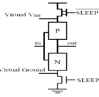
Figure 1.Power gating circuit.In the ACTIVE state, the sleep transistor is on. Therefore, the circuit functions as usual. In the STANDBY state, the transistor is turned off, which disconnects the gate from the ground. To lower the leakage, the threshold voltage of the sleep transistor must be large. Otherwise, the sleep transistor will have a high leakage current, which will make the power gating less effective. Additional savings may be achieved if the width of the sleep transistor is smaller than the combined width of the transistors in the pull-down network. In practice, Dual Vt CMOS or Multi-Threshold CMOS (MTCMOS) is used for power gating. In these technologies there are several types of transistors with different Vt values. Transistors with a low Vt are used to implement the logic, while high-Vt devices are used as sleep transistors.
To guarantee the proper functionality of the circuit, the sleep transistor has to be carefully sized to decrease the voltage drop across it when the sleep transistor is turned on. The voltage drop decreases the effective value of the supply voltage that the logic gate receives. In addition, it increases the threshold voltage of the pull-down transistors due to the body effect. This phenomenon in turn increases the high-to-low transition delay of the circuit. The problem can be solved by using a large sleep transistor. On the other hand, using a large sleep transistor increases the area overhead and the dynamic power consumed for turning the sleep transistor on and off. Note that because of this dynamic power consumption, it is not possible to save power for very short idle periods. There is a minimum duration of the idle time below which power saving is impossible. Increasing the size of the sleep transistors increases this minimum duration.
3.5T TSPC D Flip Flop:
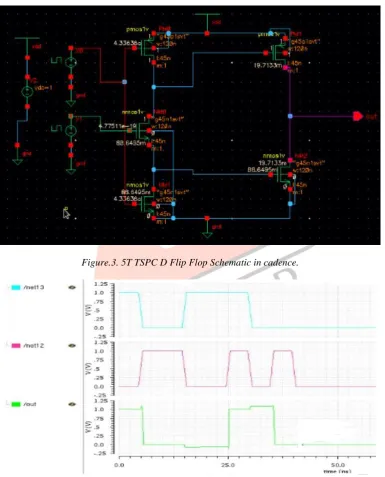
In 5T TSPC D Flip Flop, TSPC stands for True Single Phase Clocked logic in which we only have one clock, and do not need an inverted clock. TSPC circuit technique uses only one phase of the clock and avoids skew problems thereby improving the performance of a digital system. There are several benefits with this technique such as the elimination of skew due to different clock phases and clock signal being generated off chip, which implies significant savings in chip area and power consumption [4]. The following figure shows the schematic of 5T TSPC D Flip Flop which is composed of 3 NMOS and 2 PMOS transistors [5, 6].
IJEDR1402048
International Journal of Engineering Development and Research (www.ijedr.org)1575
Figure.3. 5T TSPC D Flip Flop Schematic in cadence.Figure 4.The output waveform for 5T TSPC D Flip Flop in cadence.
IJEDR1402048
International Journal of Engineering Development and Research (www.ijedr.org)1576
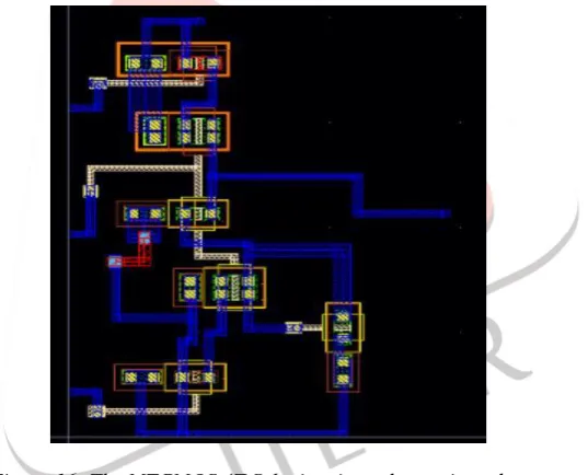
Figure.5: 5T TSPC D Flip Flop layout in cadence.4. 5T TSPC D Flip Flop with MTCMOS:
Multithreshold voltage CMOS (MTCMOS) reduces the leakage by inserting high-threshold devices in series to low Vth circuitry [7].A sleep control scheme is introduced for efficient power management. In the active mode, SL is set low and sleep control high transistors (sleep and sleep bar) are turned on. Since their on-resistances are small, the virtual supply voltages (VDDV and VSSV) almost function as real power lines. In the standby mode, SL is set high, sleep and sleep bar are turned off, and the leakage current is low [8]. This is the general mechanism of MTCMOS technique, which is employed in this work.
The following figure shows the schematic of 5T TSPC D Flip Flop with MTCMOS technique. Two sleep transistors P3 and N4 are used in this circuit. The transistor N4 is supplied with signal SL (sleep) and transistor P3 is supplied with signal SL’ (complement of sleep). SL and SL’ transistors are supplied with high threshold voltages. When SL signal is low SL’ is high, there will be no current flow in low threshold voltage main circuit. When SL is high and SL’ is low circuit works in normal mode.
Fig.6: Schematic of 5T TSPC with MTCMOS D Flip Flop. The truth table of 5T TSPC with MTCMOS D Flip Flop is shown below.
CLK D SL P1 N1 N2 P2 N3 P3 N4 Q
1 0 0 ON ON OFF OFF ON ON OFF 0
1 0 1 ON ON OFF OFF OFF OFF ON 0
1 1 0 OFF ON ON ON OFF ON OFF 1
1 1 1 OFF ON ON ON OFF OFF ON 1
0 0 0 ON OFF OFF OFF OFF ON OFF 0
0 0 1 ON OFF OFF OFF OFF OFF ON 0
0 1 0 OFF OFF ON OFF OFF ON OFF 0
0 1 1 OFF OFF ON ON OFF OFF ON 0
IJEDR1402048
International Journal of Engineering Development and Research (www.ijedr.org)1577
Fig.7: Schematic of 5T TSPC with MTCMOS D Flip Flop in cadence.Figure.8: The output waveform for 5T TSPC MTCMOS D Flip Flop in cadence.
IJEDR1402048
International Journal of Engineering Development and Research (www.ijedr.org)1578
Figure.9: The 5T TSPC MTCMOS D Flip Flop Layout in cadence.The below table shows the comparisons between the 5T TSPC D Flip Flop and 5T TSPC MTCMOS D Flip Flop results while giving diffèrent voltages.
PARAMETERS 5T TSPC D-FLIP FLOP 5T TSPC D-FLIP FLOP WITH
MTCMOS VOLATAGES (V) 1.8 1.2 1.8 1.2 POWER (uw) 3.68 3.39 1.66 1.03 DELAY (ns) 0.140 0.131 0.149 0.152
POWER DELAY PRODUCT (fj) 0.515 0.444 0.247 0.156 TABLE.3: Shows the comparisons between the 5T TSPC D Flip Flop and 5T TSPC MTCMOS D Flip Flop results.
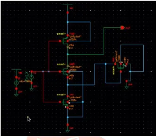
5. 4T SCHMITT TRIGGER:
The 4T Schmitt trigger circuit is configured by a combination of three NMOS (N1, N2 and N3) and one PMOS (P1), CMOS circuit is used for low power consumption operation, there is no direct connection between power supply Vdd and ground Vss as PMOS is connected to power supply and circuit output, on other hand, NMOS is connected to output and ground terminal, there is no static power due to no direct connection between power supply to be ground [9].
Figure.10: Hysteresis plot Hysteresis of the Schmitt trigger is defined as [10],
IJEDR1402048
International Journal of Engineering Development and Research (www.ijedr.org)1579
Figure.11: The 4T Schmitt trigger in cadence.Figure 12 shows the input–output waveform of Schmitt trigger in Nanoscale technology using cadence tool, when input voltage Vin = 0.7 V and Vth = 0.7 V.
Figure.12: The input–output waveform of Schmitt trigger in cadence.
IJEDR1402048
International Journal of Engineering Development and Research (www.ijedr.org)1580
Figure.13: The 4T Schmitt trigger layout in cadence.6. SCHMITT TRIGGER WITH MTCMOS:
For maintaining the low power in CMOS circuit, we are using MTCMOS technique. In MTCMOS technique, using the high threshold sleep transistor (hvt) on top of the Schmitt trigger logic transistor of low threshold (lvt) become disconnected from power supply. Transistor having low threshold voltage (low-Vth) is used to design 4T Schmitt trigger logic as shown figure.14
Figure.14: The MTCMOS 4T Schmitt trigger in cadence.
IJEDR1402048
International Journal of Engineering Development and Research (www.ijedr.org)1581
Figure.15: The output waveform for MTCMOS 4T Schmitt trigger in cadence.The figure 15 shows the output waveform for MTCMOS 4T Schmitt trigger in cadence. The waveform states that whenever the sleep signal is in ON state or in high state only the Schmitt trigger converts the given sinusoidal signal into square wave.
Figure.16: The MTCMOS 4T Schmitt trigger layout in cadence.
The below table shows the comparisons between the 4T Schmitt trigger and the MTCMOS 4T Schmitt trigger results with different voltages.
PARAMETERS: 4T SCHMITT TRIGGER 4T SCHMITT TRIGGER WITH
MTCMOS VOLATGES (V) 0.9 0.7 0.9 0.7
POWER (nW) 203.4 156.2 100.5 80.62
DELAY (ns) 417.5 358.2 301.0 409.2
POWER DELAY PRODUCT (fj)
84.91 55.95 41.12 24.29 TABLE 4: Shows the comparisons between the 4T Schmitt trigger and the MTCMOS 4T Schmitt trigger results. 7.CONCLUSION
IJEDR1402048
International Journal of Engineering Development and Research (www.ijedr.org)1582
virtuoso Tool. Hence from the results we can say that as the technology is scaled down power dissipation decreases and propagation delay increases. From the details of Figure of merit MTCMOS based circuits has least power delay product when compared to the original circuits, which gives rise to best performance. Hence, the circuits designed using MTCMOS are suitable for high performance applications like level converters, microprocessors, clocking systems counters, oscillators and wave shaping digital & analog communication circuits.Bibliography
[1] Designing Low-Power Circuits: Practical Recipes by Luca Benini Giovanni De Micheli Enrico Macii.
[2] Pradeep Singla and Naveen Kr. Malik, “A cost- effective design of reversible programmable logic array” International Journal of Computer applications Vol.41 (15), pp.41-46, 2012.
[3] Y. Lee, D. K. Jeong, and T. Kim, “Simultaneous control of power/ground current, wakeup time and transistor overhead in power gated circuits,” in Proc. ICCAD, 2008, pp. 169–172.
[4] Bill Pontikakis, A Novel Double Edge Triggered Pulse Clocked TSPC D Flip Flop for High Performance and Low Power VLSI Design Applications. Deptt of Electrical and Computer Engineering, Concordia University, Canada, 2003. [5] M. A. Hernandez and M. L. Aranda, ―A Clock Gated Pulse –Triggered D Flip-Flop For Low Power High Performance
VLSI Synchronous Systems,‖ Proceedings of the 6th International Caribben Conference on devices, circuits and systems, Mexico, Apr. 26-28, 2006.
[6] Anis M., Areibi, Mahmoud, and Elmasry, "Dynamic and leakage power reduction in MTCMOS circuits". Design Automatio Conference, 2002. Proceedings 39th (ISBN 1-58113-461-4): 480–485, 2002.
[7] J. Kao, A. Chandrakasan, and D. Antoniadis, “Transistor sizing issues and tool for multi-threshold CMOS technology,” in Proceedings of ACM/IEEE. Design Automation Conference, pp 495-500, 1997.
[8] Kaushik Roy, Saibal Mukhopadhyay, and Hamid Mahmoodi Meimand, “Leakage Current Mechanisms and Leakage Reduction Techniques in Deep- Submicrometer CMOS Circuits”. Proceedings of the IEEE, vol. 91, no. 2, February 2003. [9] Kundra Swati, et. al, “Low power Schmitt Trigger “ISSN 2222-1727 Vol.3, No.2, 2012.