-TeleVided
TS 160S/TS 160SH
Technical Reference
TS 1605/16058 Technical Reference
Te1eVideo®Te1e-PC and Te1e-XT
Models TS 1605 and TS 16058 Technical Reference Manual
Copyright
TeleVideo Part Number 123181-01 Rev. A 15 June 1984
This document contains reference information to be used in
specifying, operating, and maintaining the TS 1605 and TS l605H
Personal Computer systems. The contents of this document are
copyrighted by TeleVideo Systems, Inc. 1984, and must not be photocopied, duplicated, or reproduced without the express written permission of TeleVideo Systems, Inc.
Disclaimer
TeleVideo Systems, Inc. reserves the right to make improvements to products without incurring any obligations to incorporate such improvements in products previously sold. Specifications and information contained in this manual are subject to change without notice.
Material describing applications of components supplied by
independent vendors such as Intel, Synertek, and Western Digital have been based in large part upon handbooks, technical manuals, and similar information distributed by such vendors. For a
complete description of those parts and the ways in which they may be used, reference should be had to vendors' texts, which will be more complete.
TS 1605/16058 Technical Reference
COMPUTER SYSTEMS DIVISION BOYER'S LIMITED WARRANTY
TeleVideo Systems, Inc. ("TeleVideo") warrants to Buyer that its products, except software, will be free from defects in materials and workmanship for 90 calendar days after date of sale.
TeleVideo's obligations under this warranty will be limited to repairing or replacing, at TeleVideo's option, the part or parts of the products which prove defective in material or workmanship, provided that Buyer gives TeleVideo prompt notice of any defect and satisfactory proof thereof.
If service is required under this warranty, Customer must return the product to an Authorized TeleVideo Dealer or the original
Dealer from which the unit was purchased. With respect to any
product or part thereof not manufactured by TeleVideo, only the warranty, if any, given by the manufacturer thereof will apply.
EXCLUSIONS
All statements, technical information, and recommendations in this document and in any manuals or related documents are
believed to be reliable, but the accuracy or completeness thereof is not guaranteed.
This limited warranty does not cover losses or damage which occurs in shipment to or from Buyer, or is due to (1) improper installation or maintenance, misuse, neglect, or any cause other
than ordinary commercial or industrial application or (.2)
adjustment, repair, or modifications by other than TeleVideo authorized personnel or (3) improper environment, excessive or inadequate heating or air conditioning, and electrical power failures, surges, or other irregularities or (4) any statements made about TeleVideo's products by salesmen, dealers,
distributors, or agents unless confirmed in writing by a TeleVideo off icer.
The foregoing TeleVideo limited warranty is in lieu of all other warranties, whether oral, written, express, implied, or
statutory. Implied warranties or merchantability and fitness for
a particular purpose will not apply. TeleVideo's warranty
obligations and buyer's remedies hereunder are solely and exculsively as stated herein. TeleVideo makes no warranty
whatsoever concerning any software products, which are sold ·as is· and ·with all faults.·
TeleVideo's liability, whether based on contract, tort, warranty, strict liability, or any other theory, shall not exceed the price of the individual unit whose defect or damage is the basis of the
claim. In no event shall TeleVideo be liable for any loss of
profits, loss of use of facilities or equipment, or other indirect, incidental, or consequential damages.
TS 1605/1605H Technical Reference
TABLE OF CONTENTS
1.
2.
3.
INTRODUCTION
. . . .
·
·
•·
FUNCTIONAL DESCRIPTION
· · ·
·
•System Board
.
.
.
. ·
·
·
·
Video Monitor Interface
·
·
·
·
Winchester Disk Controller Board
CIRCUIT DESCRIPTION
· ·
· ·
·
·
CPU Controller Section •
Main Memory • • • •
Interrupt System • • • • • • • •
DMA • • • • • • • • • •
• •
·
•·
·
· ·
·
.
Serial I/O • • • • • • • • • • .
Parallel Printer Port • • •
Keyboard Interface • • • • • • • • • Speaker Drive System • • • • • • • •
Input/Output Channel • • • •
Floppy Disk Controller • • • Winchester Controller Interface Winchester Disk Controller Board •
·
•·
·
·
•·
·
•·
·
·
·
·
·
·
· ·
·
•· ·
·
·
· . .
System/Controller Interface • • •
Operations With Buffer RAM • • • • • • • • •
Writing Disk Data • • • • • •
Reading Disk Data
Video Section • • •
•
.
·
•· .
·
.
Video Memory • • • • • • • • • •
CRT Controller and Character Generator •
Video Module • •
.
.
. . .
1.1 2.1 2.3 2.6 2.6 3.1 3.3 3.7 3.10 3.12 3.15 3.18 3.20 3.22 3.25 3.25 3.27 3.28 3.29 3.29 3.31 3.34 3.35 3.36 3.37 3.40
4. HARDWARE PROGRAMMING. • • • • • • • • • • • • • • • 4.1
System Interrupts • • • • • • • • • • •
Programmable Interval Timer Programming
Memory • • • • • • • • • • • • • • • • • • • • • • Programmable Peripheral Interface Device •
Speaker Interface • • • • • • • • • • • •
Keyboa rd. • • • • • • • • • • • • • • • • • •
Video Section • • • • • • • • • • • •
Controller Programming • • • • • • • • • • •
Mode-Select Register • • • • • • • • • •
Color-Select Register • • • • • • •
Status Register • • • • • • • • • •
Alphanumeric Mode • • • • • • • • • • • • •
TS 1605/16058 Technical Reference
5.
Command Status Register 3 • • • • • • • • •
Serial Port • • • • • • • • • • • • • • • • •
Line-Control Register • • • • • • • • •
Programmable Baud Rate Generator • • • • • • Line-Status Register • • • • • • • • • •
Interrupt-Identification Register • • •
Interrupt-Enable Register • • • • • • • • • • •
Modem-Control Register • • • • • • • • •
Modem-Status Register • • • • • • • • • • •
Receiver Data Register • • • • • • • • •
Transmitter Holding Register • • • •
Parallel Port • • • • • • • • • • • . • • • •
liD Channel • • • • • • • • • • • • • • •
Winchester Disk Controller Board . • •
Task File Register Functions • • • •
ROM BIOS AND SYSTEM USAGE
ROM BIOS • • • • • • • . • . • • . • • • • • •
Video liD - Interrupt %10 • • •
Character Handling Routines • • • . • •
Graphics Interface Routines • • • • • • • • • •
Equipment Check - Interrupt %11 • • • • • •
Memory - Interrupt %12 • • • • • • • • •
Diskette liD - Interrupt %13 • • • • • •
.
.
Fixed Disk liD - Interrupt %13 • • • • •
RS-232C Communications - Interrupt %14 •
Keyboard - Interrupt %16 . . • • • •
Printer - Interrupt %17 • • • . • • • • • •
Bootstrap - Interrupt %19 • • •
Time of Day - Interrupt %lA • • • • • •
Keyboard Break Address - Interrupt %lB •
Timer Tick - Interrupt %lC • • • • • • •
Video Parameters - Interrupt %lD • • • •
Diskette Parameters - Interrupt %lE • • • •
Graphics Character Extensions - Interrupt %IF • •
Interrupt %40 • . . . • • . . • • . • .
Fixed Disk Parameters - Interrupt %41 • • •
BIOS Memory Usage • • • • • • •
Keyboard Encoding and Usage . • •
Extended Codes • • • • • • . • • • • • •
Shift States • • • • • • . . • • • •
Special Key Combinations • • • • • • • •
APPENDICES
A. References
·
·
· · ·
·
·
·
·
· · · ·
·
· ·
B. liD Port Addresses
·
· ·
·
· · ·
·
· ·
·
·
C. Power-On Self Test
.
.
. .
.
. .
.
•. .
.
D. ASCII Character Code Chart
·
·
·
..
· ·
·
·
E. Glossary of Acronyms
· ·
·
·
·
·
·
F. Connector Pin Assignments
·
·
·
·
·
·
G. Disk Drive Specifications.
·
·
·
·
·
· ·
•H. Jumpers
.
· ·
·
·
·
· ·
·
·
·
·
·
·
·
·
· · ·
I. Schematics
·
·
·
·
·
· ·
·
·
· · ·
·
·
4.27 4.28 4.28 4.30 4.31 4.32 4.33 4.34 4.35 4.36 4.36 4.37 4.39 4.41 4.41 5.1 5.1 5.2 5.3 5.3 5.4 5.4 5.4 5.5 5.7 5.8 5.9 5.9 5.9 5.10 5.10 5.10 5.10 5.10 5.10 5.10 5.11 5.11 5.14 5.14 5.15 A.l B.2 C.4 D.5 E.6 F.7 G.12 H.13 1.14
TS 1605/16058 Technical Reference
LIST OF FIGURES
2-1 3-1 3-2 3-3 3-4 3-5 3-6 3-7 3-8 3-9 3-10 3-11 3-12 3-13 3-14 3-15 3-16 3-17 4-1 4-2 4-3 5-1 D-l
TS 1605 System Board • • • • • • • • • • • • • • •
Block Diagram of the Main Board • • • • •
Control Section • • • • • • • • • • • • • • •
RAM Main Memory • • • • • • • • • • • • • • • • •
Interrupt System • • • • • • • • • • • • • • • • •
DMA Control • • • • • • • • • • • • • • • . • • •
DMA Memory Address Generation • • • • • •
Asynchronous Communications • • • • • • •
I/O Interface Diagram • • • • • • • • • •
Parallel Printer Logic • • • • • • • • • • • • • • Keyboard Circuit • • • • • • • • • • • • • • •
Speaker Drive System • • • • • • • • • • • • • • • Floppy Disk Controller • • • • • • • • • •
Winchester Disk Controller Board Block Diagram
Writing Disk Data • • • • • • • • • • • • • •
Reading Disk Data • • • • • • • • • • • • • •
CRT Controller and Video Memory Block Diagram.
Video Monitor • • • • • • • • • • • • • •
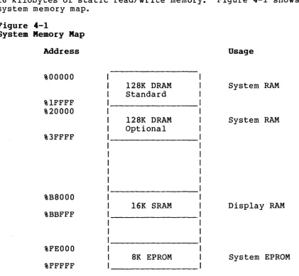
System Memory Map • • • • • • • • • • • • • •
Software-Selectable Palettes • • • • • • •
Graphic Memory Addresses • • • •
BIOS Memory Map • • • • • • • • • • • • •
ASCII Character Code Chart • • • • • • • • • •
LIST OF TABLES
2-1 I/O Port Addresses
·
·
·
·
·
·
3-1 CPU Devices
·
·
· ·
·
·
·
·
·
·
·
·
·
3-2 Main Memory Components
·
·
·
· ·
·
·
·
3-3 I/O Component
·
·
·
·
·
·
·
· · ·
3-4 Major Parallel I/O Components
·
· ·
·
·
·
3-5 Keyboard Interface Components
·
·
· ·
·
· ·
·
3-6 Floppy Disk Controller Components
·
·
·
· ·
·
3-7 Winchester Controller Interface Components
· ·
· ·
3-8 System/Controller Interface Components
· · · ·
3-9 Write from Buffer RAM •
·
· ·
· ·
·
·
3-10 Read from Buffer RAM
· ·
· ·
·
·
·
·
·
· ·
3-11 Writing from Buffer RAM
· ·
· · ·
·
·
·
·
3-12 Disk Data
.
·
·
·
·
·
·
·
·
·
·
·
3-13 Video Memory Components
·
·
·
·
· ·
·
· ·
3-14 CRT Controller and Character Generator Components.
4-1 Hardware Interrupt Listing
·
· ·
·
·
·
·
· ·
·
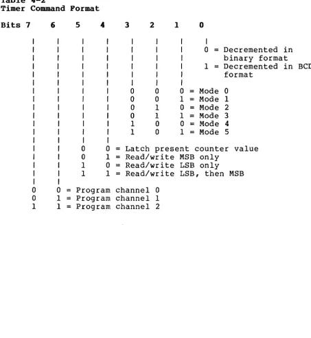
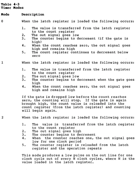
4-2 Timer Command Format
·
·
· ·
· · ·
4-3 Timer Modes
· · · ·
·
·
·
· ·
·
·
· ·
4-4 8255A-5 I/O Bit Map
· ·
·
· ·
·
·
·
·
·
·
4-5 Keyboard Scan Codes
·
·
· · ·
4-6 CRT Controller Registers
·
•· ·
·
·
·
· ·
4-7 Mode-Select Register • • • •
·
· ·
4-8 Mode-Select Register Summary
·
· ·
TS 1605/1605B Technical Reference . 4-13 4-14 4-15 4-16 4-17 4-18 4-19 4-20 4-21 4-22 4-23 4-24 4-25 4-26 4-27 4-28 4-29 4-30 4-31 4-32 4-33 4-34 4-35 4-36 4-37 5-1 5-2 5-3 5-4 5-5 B-1 E-l F-l F-2 F-3 F-4 F-5 F-6 F-7 F-8 F-9 F-IO F-ll
Medium-Resolution Byte Usage • • • • • • •
Medium-Resolution Color Selection Logic • • •
Digital-Output Register. • • • • • • • • •
FDC Status Register • • • • • • • • . • •
FDC Command Summary • • • • • .• • • • • •
FDC Command Symbols • • • • • • • • •
UART I/O Register Addresses • • • • •
Line-Control Register • • • • • • •
Divisor Latches • • • • • • •
Divisor Baud Rates • • • • • • • • • • • • • • Line-Status Register • • • • • • • • • • • Interrupt-Identification Register
Interrupt Control Functions • • • • • • • • •
Interrupt-Enable Register • • • • • •
Modem-Control Register • . • • • • • • • • • • Modem-Status Register • • • • • • • • • • • • •
Receiver Data Register • • • • • • • • • •
Transmitter Holding Register • • • • • • • • •
Data Output Port • • • • • • • • • ~ •
Output Control Port • • • • • • • • • • • • •
Control Signal Input Port • • • . • • • •
I/O Channel Signals • • • • • • • • • • • • •
TS 1605 Registers • • • • • • • • • •
Error Register Bit Assignments • • • • • •
Command Register Format •.•• . • • • • • • •
Interrupt Vectors • • • • • • • •
Character Codes • • • • • • • • •
Numeric Keypad Keys . • • • • • . • •
Keyboard Extended Codes • • • • • • •
Special Key Combinations • • • • • • •
lID Port Addresses • • • • • • • • • • • •
Glossary of Acronyms • • • • • • •
Connector PI (Serial I/O) • • • • • •
Connector P2 (Parallel I/O) • • • • • • •
Connector P3 (I/O) Channel) • • •
Connector PS (Power Supply) • • • • • • • • •
Connector P7 (Floppy Disk Controller) • • • •
Connector P9 (Programmable Interval Timer) Connector P8 (Winchester Hard Disk Controller Interface) • • • • • • • • • • • • • • • • • • Connector PII (Keyboard Interface) • • • • • • Connector VPl (Composite Color Monitor Port) • Connector VP2 (RGB Color Monitor Port) • • • • • • Connector VP3 (Standard TeleVideo Video Monitor) •
4.15 4.15 4.16 4.17 4.17 4.23 4.28 4.29 4.30 4.30 4.31 4.32 4.33 4.33 4.34 4.35 4.36 4.37 4.37 4.38 4.38 4.39 4.41 4.42 4.44 5.1 5.12 5.13 5.14 5.15 B.2 E.6 F.7 F.7 F.8 F.9 F.9 F.lO F.IO F.IO F.ll F.ll F.ll
TS 1605/16058 Technical Reference Introduction
1. INTRODUCTION
The TeleVideo TS 1605 and TS 16058 computer systems are based on the Intel 8088 microprocessor, using the same circuit board in different configurations. The 8088 microprocessor is an 8-bit external, l6-bit internal device with a 20-bit address bus.
The TS 1605 is an integrated stand-alone system with two slim
line floppy disk drives. The vertically-mounted floppy disk
drives are 48 TPI drives with a formatted storage of 360 kilobytes per drive.
The system board contains an RS-232 serial I/O port, configured for asynchronous communication. An IBM-compatible parallel I/O port is configured for a parallel printer or other general
communications device. Keyboard I/O is handled by a programmable
peripheral interface device. An IBM-type I/O channel can
interface with any I/O devices not on the system board.
The TS l605H is similar to the TS 1605, except that it features a 3 1/2-inch 10 megabyte Winchester hard disk drive and a single
floppy disk drive. The controller for the Winchester drive is
contained on a separate board.
Standard main memory for the TS 1605 is 128 kilobytes, expandable to 256 kilobytes with an expansion board or added memory chips.
Standard main memory for the TS l605H is 256 kilobytes. An
8-kilobyte system ROM device is used for system power-on self-test, disk drive bootstrap loader, and input/output drivers.
The color/graphics monitor interface, capable of operating in black and white or color, is designed around the Synertek 6845R CRT controller. Graphics memory uses 16 kilobytes of static RAM. Resolution is 640 pixels horizontal by 200 pixels vertical for the monochrome graphics display and 320 pixels by 200 pixels for
the color graphics display. The alphanumeric display is 25 lines
by 80 columns of characters, featuring hidden attributes for the monochrome display, and eight background colors and sixteen
foreground colors for the color display.
The TS 1605 and TS 16058 use an IBM-style keyboard and standard TeleVideo video driver circuits.
TS 1605/1605B Technical Reference Description
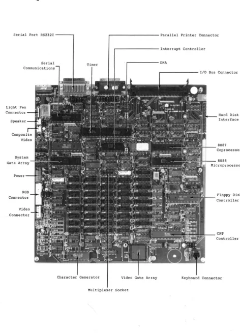
2. FUNCTIONAL DESCRIPTION
The TS 1605 and TS l605H are single-board systems (see Figure 2-1). The TS l605H has interface circuitry for a Winchester hard disk controller board.
TS 1605/16059 Technical Reference Description
Figure 2-1
TS 1605 System Board
Serial Port RS232C ---...,
Serial Communications
Light Pen Connector
Speaker
Gate Array
Power --I~'II
RGB Connector
Connector
Timer
Character Generator
, . . . . - - - -Parallel Printer Connector
, . . . . - - - I n terrupt Controller
, . . . . - - - -DMA
r - - - 1/0 Bus Connector
Video Gate Array
Hard Disk Interface
8087
~~--coprocessor
~-:---8088
Microprocessor
Floppy Disk Controller
CRT Controller
Keyboard Connector
TS 1605/16058 Technical Reference Description
SYSTEM BOARD
The system board contains circuits for control and video
processing functions. An Intel 8088 8-bit HMOS microprocessor device performs logical and computational functions of the
running software, handles graphics processing, and updates video memory.
Arithmetic and comparison operations can be handled with the
addition of an optional Intel 8087 Numeric Data Processor. The
CPU and numeric data processor operate at a frequency of 4.77 MHz, which is divided down from a 14.31818-MHz crystal through an Intel 8284A Clock Generator.
An Intel 8237A-5 DMA controller device allows external devices to
transfer information directly to or from system memory. The DMA
provides four channels of 16-bit address,space. Twenty bits of
address space can be obtained by programming a hardware latch for
the highest four bits of address. One DMA channel is used to
refresh dynamic memory. The three remaining DMA channels are used
for data transfers of the floppy disk, hard disk, and I/O channel.
All necessary signals for dynamic memory reads and writes are
generated by the TeleVideo Memory Control Gate Array. The memory
control gate array works together with an Intel 8288 Bus Controller to control timing when the DMA uses the buses.
An Intel 8259A Interrupt Controller provides eight prioritized levels of interrupt for the system.
Main memory is configured in 64K x 1 dynamic RAM chips with a
minimum data access time of 150-200 nanoseconds. Standard
main memory capacity is 128 Kbytes of dynamic RAM for the TS 1605 and 256 Kbytes for the TS 1605H. Main memory can be expanded in three ways:
*
*
*
Up to 256 Kbytes on th,e TS 1605 by adding 64K x 1 RAM chips into the existing sockets on the system board.
Up to 512 Kbytes by replacing the 64K x 1 RAM chips with 256K x 1 RAM ch ips (64K chips cannot be mixed with 256K
chips). This requires installing a multiplexer 74LS158
chip into the existing socket on the system board (see the Multiplexer Socket in Figure 2-1).
Up to 640 Kbytes by connecting an expansion board via a 64-pin ribbon cable to the expansion slot on the system board
(see the I/O Bus Connector in Figure 2-1). Before connecting
TS 1605/1605B Technical Reference Description
Read-only memory is configured in a single 8-Kbyte ROM chip. This memory contains codes for system boot and power-up
diagnostics. Graphics memory has 16 kilobytes of static RAM.
The liD ports are decoded with two devices. liD port decoder #1
enables the programmable interrupt controller, programmable DMA controller, programmable interval timer, and programmable
peripheral interface. liD decoder #2, a read-only device, enables
the floppy disk controller, serial liD port, parallel liD port,
and Winchester disk controller board.
A list of liD port addresses is contained in Table 2-1 and
Appendix B. The liD port decoders are addressed on lines XAS
through XA8 and A2 through A9. The decoder enables, along with
the internal I/O device registers, configure the system and pass
data to system peripheral devices.
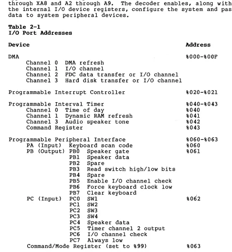
Table 2-1
I/O Port Addresses
Device
DMA
Channel 0 Channel 1 Channel 2 Channel 3
DMA refresh
liD channel
FDC data transfer or liD channel
Hard disk transfer or liD channel
Programmable Interrupt Controller
Programmable Interval Timer Channel 0 Time of day
Channel 1 Dynamic RAM refresh Channel 3 Audio speaker tone Command Register
Programmable Peripheral Interface
PA (Input) Keyboard scan code
PB (Output) PBO Speaker gate
PBl Speaker data
PB2 Spare
PB3 Read switch highllow bits
PB4 Spare
PBS Enable liD channel check
PB6 Force keyboard clock low
PB7 Clear keyboard
PC (Input) PCO SWI
PCl SW2
PC2 SW3
PC3 SW4
PC4 Speaker data
PCS Timer channel 2 output
PC6 liD channel check
PC7 Always low
CommandlMode Register (set to %99)
Te1eVideo Systems, Inc.
Address
%OOO-%OOF
%020-%021
%040-%043 %040
%041 %042 %043
%060-%063 %060
%061
%062
%063
TS 1605/16058 Technical Reference Description
DMA Page Register %OSO-%OS3
NMI Mask Register %OAO
To enable NMI, write data %SO into address %OAO To disable NMI, write data %00 into address %OAO
Serial Port (Primary)
Tx Buffer/Rx Buffer/ Divisor Latch Interrupt Enable/Divisor Latch MSB Interrupt Identification Register Line Control Register
Modern Control Register Line Status Register Modern Status Register
Floppy Disk Control Port Select drive A
Select drive B Reset 8272A FDC
Disable interrupt/DMA operation Enable interrupt/DMA operation Turn on both motors
Floppy Disk Controller
FDC Main Status Register FDC Data Register
Parallel Data Port (Read/write)
Parallel Control Port (Read/write) STROBE (-)
AUTO FD XT INIT (-) SLCT IN (-)
INTERRUPT ENABLE
Parallel Status Port (Read only) ERROR (-)
SLCT PE
ACK (-) BUSY (-)
Winchester Disk Control Register To enable interrupt:
To disable interrupt: To enable DMA operation: To disable DMA operation:
LSB
%3FS-%3FF %3FS
%3F9 %3FA %3FB %3FC %3FD %3FE
%3F2 DO = 0 DO
=
1D2
=
0 D3=
0 D3=
1D4
=
1 or D5=
1%3F4-%3F5 %3F4
%3F5
%3BC
%3BE DO Dl D2 D3 D4
%3BD D3 D4 D5 D6 D7
%OEO D6
=
1D6
=
0 D7=
1TS 1605/l605H Technical Reference Description
Winchester Disk Read Data Error flag Sector count Sector number Cylinder low Cylinder high SDH
Controller Board Task File Register Write Data
Write precomp cylinder Sector count
Sector number Cylinder low Cylinder high SDH
Status register Command register
%330-337 %330 %331 %332 %333 %334 %335 %336 %337
The serial I/O port is contained in a WD8250 serial I/O device as
a general purpose, asynchronous RS-232 port. This device can be
programmed for data rates of from 50 baud to 9600 baud. Current-loop operation is also supported in the serial port.
A general-purpose parallel I/O port provides a parallel printer
interface. Interrupts are enabled or disabled by program
control.
The I/O channel is used to interface to any I/O devices not on
the system board. The I/O channel provides data and address
lines, control signals, interrupt lines, and DMA control lines.
Devices are addressed using I/O mapped address space. The I/O
channel provides power to expansion slot Jl.
An Intel 8272A Floppy Disk Controller device and FDC9229B Data Separator support double-sided, double-density format for the system floppy disk drives.
An eight-section DIP switch pack can be read by program control through an Intel 8255 Programmable Peripheral Interface device. The DIP switch provides all system information to firmware and
software. Settings for this switch pack are given in the system
User's Manual.
Scan codes from the keyboard, which are in serial data format, are converted into parallel data format and read by the
programmable peripheral interface. The peripheral interface also controls the audio speaker tone and enable/disable I/O channel er ror check.
VIDEO MONITOR INTERFACE
The video monitor interface is configured around the Synertek
6845R CRT Controller. The interface is capable of operating in
either monochrome or color.
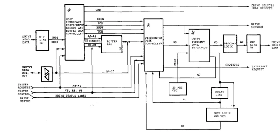
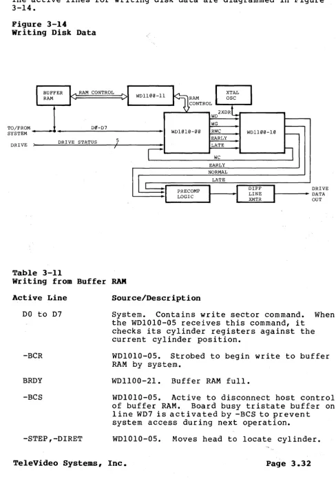
WINCHESTER DISK CONTROLLER BOARD
A Western Digital WDIOIO-05 Controller on a WDIOOO-05 3 1/2-inch Winchester Disk Controller board is used to interface with the 5 1/4-inch Winchester hard disk drive.
TS 1605/16058 Technical Reference Circuits
3. CIRCUIT DESCRIPTION
This section contains circuit descriptions of the major
functional blocks of the TS 1605 and TS 1605H system board, as well as a description of the WD1000-05 Winchester Disk Controller Board.
The system board contains the CPU, main memory, I/O ports, controllers, and video display circuits for the system.
~ Il't'Il ~
tD
...
en....
O~tD nc:
....
<I ;w.., G\
....
tD 0Q, 0 U1
tD ... ·W
"-0 S» I
....
~
....
G\en
..,
0'< S» U1
til IS
=
rt
tD, 0 ~
IS H\ tD
til n
..
rt t:rt:r CS
... tD
....
CS n
n
=-
S»• S»
....
....
CS ~
Il' H\
0 tD
DJ
..,
..,
tDc" CS
n
tD
a ~
n
....
..,
n
~ c:
S»
....
~ rt
tD til
eN
TS 1605/16058 Technical Reference Circuits
CPU CONTROLLER SECTION
The controL section block diagram illustrates the processing of
the control, data, and address buses. The 8284 time (U63) sends
three signals to the 8088 and 8087 processors. The clock signal
is a 4.77 MHz signal with a 33% duty cycle. The RESET .signal
halts CPU operation. The RDY signal inserts wait states between times T3 and T4 of the system bus cycle.
There are four signals that tie the 8088 to the 8087
co-processor. QSO and QSI are input to the 8087 so it can monitor
the status of the 8a88's internal queue. The RQ/GTI signal of
the 8088 is connected to the RQ/GTO pin of the 8087. This signal
allows the co-processor (8087) to take over the local bus to perform its functions. The TEST signal to the 8088 is examined
by a WAIT instruction. If the TEST input is LOW, execution
continues. Otherwise, the processor waits in an "idle" state.
Signals SO-S2 leave the 8088 with status information used and
decoded by the 8288 bus controller. When decoded by the bus
controller, these signals become the control bus signals lORD,
IOWC, MRDC, and MWTC. However, during a DMA cycle, bidirectional
transceiver U44 is the path for control bus signals which come from the DMA controller.
The 8288 bus controller also issues control signals DEN, DT/R,
and ALE. The DEN signal enables bidirectional transceiver U45
which enables data onto the system data bus at T3 of the bus
cycle. ~he DT/R signal controls the direction of the data flow
through bidirectional transceiver U45. When active HIGH, the ALE
signal latches address lines AO-A19 into latches U29, U30, and
U3l. These address lines are then buffered by U2l, U22, and U23.
XTAL 1 4.31818 MHZ
r1Qb
C§) 8284 -tog PI ~ tD W • ~ IOWC MRDC MWTC II
CLKI
-
8288CLK -< 8088
-
-S~ - S2
ROY r\
'---\
CONTROL BUS ~ 74LS243 MEMW---
....RST .... @D
.4
r-tf
@D
- - - - , D E N
MEMR ....
...
-lOW
-...
r+ RG/GT
r\
-ifWTR
Tt:"ST Qs0 QSl ~!
~
-_ D T / R ,...- ALE
-lORD
----
G2D
'OMA cye
1
-
0'\BUSY QS0 QS 1 r l
Cl
~ RG/GT
.:t:
R S T @ D
~
l--'- IL--.
t...
'&i\_.4
Cl__ RDY NDP
.:t: I"""'"
'11"11' If'
.~
r
{Ul3§) - )r
1:u10DI
L---:---=-=-=---~ ADDRESS BUS A~ - A19 __
... ALE ~ ~ II'
'--"---\- 7 4 L S 3 73
@Y
(I)
- - CLK
::J
-8087_ trl
H
.:t:
U
0
-
r
@) XA~ -XA~
@V
r-~
H
~
DIRI"'"
INTA
RFRESH
0 INT
CE
..
•l\r
KEYBD1
I/O CH
2 PIC
74LS245
I/O CH
- 3
-\
SERIAL P~ 4 8259
)I _lA
HARD DISK
GiD
/ J ~5
~
FLOPPY DISK _ 6
'ill'"
J - If'
PARLLEL PORT
7 DEN
-f\
t--• 1---'
A~ - A19 J
74S241
-
r~
DATA BUS D~ - 07
"
C(
-\
74LS245 AIDDt>
/ DD~
...
-....
1\
-J
TRANSCEIVERCQ~ ~
..
..
,
-
-
]
CPU CYC
n~ I-i
0
....
til CJ ~rt C
...
...
...
G\0 tD C
...
VIW
"'-till
...
tDN G\
n C
rt VI
TS 1605/1605B Technical Reference Circuits
The major components of the CPU Controller section are:
U55 U41 U63
U29,U30,U31 U45,U14 U21,U22,U23 U39
U28 U40 U27
Intel 80B8 CPU System Microprocessor Intel 8087 Numeric Data Processor Intel 8284A Clock Generator
Address Latches, #1,#2,#3 Transceivers, #1,#2
Address Buffers, #1,#2,#3
Intel 8259A Programmable Interrupt Controller Intel 8237A-5 Programmable DMA Controller Intel 2764 System ROM
Intel 8254 Programmable Interval Timer
Table 3-1 lists the devices or lines on the CPU and their description.
Table 3-1 CPO Devices
Device or Line
8088 CPU
-RD
RDY
-RQ/GTO,-RQ/GTI
-LOCK
Source/Description
Operated in the maximum mode, the CPU handles central processing functions, graphics
display-related processing, and all writes to
video memory. CPU timing conforms to the
standards shown in the Intel Component Data Catalog.
CPU. Read signal indicates that the CPU is
performing a memory or 1/0 read cycle.
CPU. Ready acknowledges that when not busy,
addressed memory or 1/0 device will
complete a data transfer. -S2,Sl,SO CPU.
Status signal is active during clock high of T4, Tl, and T2 and is returned to the passive state (1,1,1) during T3 or during Tw when ROY is high. Status signals are used by bus
controller to generate all memory and 1/0
access control signals.
RequestlGrant signals are used by other
local bus masters to force the CPU to release the local bus at the end of the CPU's current bus cycle.
CPU. This signal indicates that other system
bus masters are not to gain control of system
TS 1605/16058 Technical Reference Circuits
Numeric Data Processor
Clock Generator
Address Latch II
Address Latch 12
Address Latch 13
Data Transceiver
Data Transceiver
Address Buffer
Address Buffer
Address Buffer
Programmable Interrupt Controller
Programmable DMA Controller
System ROM
Programmable Interval Timer
Provides instructions and data types for high-performance numeric applications. Serves as a co-processor to the CPU.
Generates the system clock for the CPU. Using a l4.3l8l8-MHz crystal, the clock generator divides down a 4.77-MHz frequency source for the CPU and numer ic da ta
processor.
Address latch II converts CPU lines ADO through AD7 to address lines AO through A7.
Address latch '2 converts CPU lines AA8
through AA15 to address lines A8 through A15.
Address latch
'3
converts CPU lines AS16through AS19 to address lines A16 through A19.
Converts CPU lines ADO through AD7 to data ' I lines DO through 07.
Converts data lines DO through 07 to data '2 lines 000 through 007.
Buffers address lines AO through A7, which II become XAO through XA7.
Buffers address lines A8 through A15, which '2 become XA8 through XA15.
Buffers address lines A16 through A19, which #3 become XA16 through XAI9.
Handles vectored interrupts for the CPU,
accepting interrupt requests from peripherals and determining priority.
Allows peripheral devices todirectly transfer information from or to system memory.
Addressed on lines XAO through XA7, XA8
through XA13, and data lines 000 through 007, system ROM allows CPU to operate without
generating wait states to the system.
A three-channel,counter-timerdevice. Channel 0 is used for time-of-day
implementation, and channel 1 times out dynamic memory refresh. Channel 2 supports tone generation for the speaker.
TS 1605/16058 Technical Reference Circuits
MAIN MEMORY
The addresses on the TS 160S/160SH RAM are multiplex. The RAM
address MUX signal selects either the Row address (RAS> or the column address (CAS> lines. For 64K x 1, U60 is not used. The total address is 16 bit - the upper 8 bits are used for column, and the lower are used for row. READ comes from memory to the
cpu. WRITE comes from the cpu to memory. Refer to Figure 3-3
t-i tD
....
tD<
....
Q, tD o til ~ m rt tD II m 'III....
::s n • MEMRRAM SEL
AIIo
D0 - 07
""
CAS"i RAS1"
RAM ADDR MUX
-XAI6 - XA3
XA8 - XAll
XA4 - XA7
XA12 - XA15
XA16 - XA17
CASl RASl CAS2 RAS2 CAS3 RS3 WE
G OIR
74LS245
~""
~
~ U96 !\
-...
I
~ S
"
~ Ul18.~
"
J 74LS158
...
I
-\
S~
~ U107
~ AI6- A8
~
"
~ 74LS158..
..
1
S
~
,
ul19~
..
7 4LS 158"
DATA BUS 016 - 07
~ 64KX8
AI6 - A8
,
or..4 (256kz8)
V'-..
016 07 !\ CAS 16 "!II :: RASI6--<: WE
~
AI6 - A8
,
... 64KX8or
... (256kz8) 016
y..
07 !\ '" CAS1 ...
- RAS1
4~ WE
~
Ar6 - A7
,
... 64KX8...
016
;a
07\ :: CAS2..
I'I~
4...-.<l WE
~ 64KX8 AI6 - A7 ~
...
016 V AI
!: CAS3 071\ -" RAS3 ~
4~ WE
)
...
t\
,
016 - 07 ~
...
-\
0r6 - 07
J
..
~
016 - 07
,
..4
.,
1\
016 - 07
..4
...
-=~
c::TS 1605/1605B Technical Reference Circuits
The major components of main memory are:
U50 U51
U128,U93,Ul19, U86,U110,U77, U101,U69
U127,U92,Ul18, U85,U109,U76, U100,U68
U126,U91,Ul17, U84,U108,U75, U99,U67
U125,U90,Ul16, U83,U107,U74, U98,U66
Te1eVideo Memory Control Gate Array Intel 8288 Bus Controller
Bank 0 Dynamic RAM
Bank 1 Dynamic RAM
Bank 2 Dynamic RAM
Bank 3 Dynamic RAM
Table 3-2 lists the components of the main memory and their description.
Table 3-2
Main Memory Components
Device or Line
Memory Control Gate Array
A16-A19
SO,Sl
-RASO, -RAS1 -RAS2, -RAS3
-CASO,-CAS1, -CAS2,-CAS3
-RAM SEL
Bus Controller
Source/Description
Generates all necessary signals for reads and writes to dynamic memory.
CPU address latch #3. Address lines to
memory control gate array. Provide address for memory data bus exchanges.
CPu. Status lines to memory control gate
array. Memory control gate array. Row
select -RAS2,-RAS3 signals to main memory. -RASO selects row address for bank 0, -RAS1 for bank 1, -RAS2 for bank 2, and -RAS3 for bank 3.
Memory control gate array. Column select signals to main memory. -CASO selects column address for bank 0, -CAS1 for bank 1, -CAS2 for bank 2, and -CAS3 for bank 3.
Memory control gate array. Control signal selects one of four banks of main memory.
TS 1605/16058 Technical Reference Circuits
-MEMR
-MEMW
INTERRUPT SYSTEM
Bus controller. Control signal into memory control gate array to generate memory reads to main memory.
Bus controller. Control signal into memory control gate array to generate memory writes to main memory.
The system can generate one of eight designated interrupts to the 8259 interrupt controller. The INT controller then issues an
interrupt signal to the CPU. Status lines -SO, -Sl, and -S2 go
from the CPU to the 8288 bus controller. The signal tells the
8259 to run an interrupt. The 8288 issues an INTA (two signal
pulses) to the 8259. The first pulse freezes the interrupt
priority in the 8259. The second pulse causes the 8259 to put an
a-bit word on the data bus to the CPU. This is a partial address
of the interrupt vector in the lower lK of system RAM.
The CPU issues a lO-bit address that accesses one of a possible
256 locations in memory. Each of these 256 memory locations
consists of 32 bits of memory. These 32 bits are segmented to
establish the current address of the interrupt subroutine.
See Figure 3-4 for a diagram of the interrupt system.
ttl
PI
\Q
tD
MEMORY CONTROL GATE ARRAY
NMIEN 19
050
8087 NP IRQ I/O CHANNEL CK
CH0 TIMER COUNTER KYBD
I/O CH I/O CH SERIAL PORT HARD DISK
8088
t - - - t N M I CPU
. . - - -... ~INTR
055
8259 HIGHEST LEVEL
a
INTERRUPT CONTROLLER 2
INTR
AVAILABLE ON THE BUS
5
SUMMARY OF INTERRUPT LEVELS
NMI I/O CHANNEL CHECK, NUMERIC PROCESSOR IRQ 0 SYSTEM TIMER OUTPUT 8254 CHANNEL 0 IRQ KEYBOARD SCAN CODE INTERRUPT IRQ 2 I/O CH
IRQ I/O CH
IRQ 4 RS-232-C SERIAL PORT
.... toa:I
::I ~.
rt'\Q tDC
...
... tD
C
ttjW
rtl
...
tn
'< rn
rt
tD
S
~ tn
....
0\0
Ut
"-....
0\0
Ut
=
~tD n
cr
::I
~.
n
PI
....
~
H'I
tD
...
tD::I
n tD
n
~.
...
n c
....
rt
TS 1605/16058 Technical Reference
DNA
There are four OMA channels, 0, 1, 2, and 3.
o
= refresh1 = optional I/O channel
2
=
floppy disk controller3
=
optional I/O channelCircuits
The OMA cycle is ini tia ted by a OMA request from one of the four
above channels. For example, if the FOC requests a OMA request,
it sends an FOC ORQ signal to the memory control gate array. The gate array issues a signal to the OMA controller. See Figures
3-5 and 3-6 for diagrams of the OMA.
t-3 tD
....
tD<
....
c" tD o en'< en
rt tD lEI en
..
....
::s n•
(.
\
V
~CPU CYC
I/O CH FDC
woc
8237CS
DMA CYC
XAg XAI 74S245 • • ~ U132 DIR
DDH
DDg
-AfJ - A19
DD.0' - DD7
+5 U26
FF REFRESH TIME OUT
CK CLR DACK .d 't
DREQ Z DACK 1 I
DD~
DACK 28237-5 DACK 3
~
V'-
\
DREQ 1
Air - A7 DREQ 2
\l-
iDREQ 3 HRQ
.,
: CS Ul28 ADSTB
I
~ G
DD{\
J 74L5373 A8 - A15
.,
U131 GR
I
OE WA
RA WB
RB
~
Q U
m
l74LS245
Vt
1\
• • Af,r - A7
~
V
U130
. DMA CYC
J
0\ r-f..x: I ~ ..x:
1\
./
~
~ ~...., ~~. cn..,
OtD ::sJ
rtw .., IOU1
....
.,
DACK .11
DACK 1 DACK 2 DACK 3
TS 1605/16058 Technical Reference
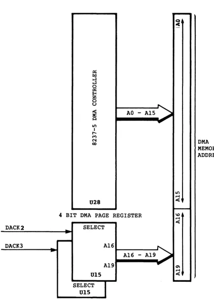
Figure 3-6
DMA Memory Address Generation
~ rz:J ~ ~ 0 ~ 8
Z
0
u
II( :E:
t:l
Ltl
I
...
('t')
N
ex)
028
Circuits
OJ
.c
-AO -
A15~
-....
Ltl r-t
11('
DMA MEMORY ADDRESS
4 BIT DMA PAGE REGISTER \OJ
r-t II(
DACK2
-
SELECT~
DACK3
-
A16A19~
~
A16
-A19
...
0\r-t
015 II(
SELECT
015
TS 1605/1605B Technical Reference Circuits
SERIAL I/O
The serial communications port interfaces with an RS-232
asynchronous communications-type device at 50 - 9600 baud rate, such as a serial printer or modem. There is a transmit and
receive line, and handshaking protocol. Figure 3-7 shows a
....
::s o•
ADDRESS BUS ADDRESS
DECODE
CHIP SELECT
DATA BUS
~
----~V
OSCILLATOR 1.8432 MHZ
EIA RECEIVERS
A
-'"
8250
ASYNCHRONOUS COMMUNICATIONS ELEMENT
CURRENT LOOP
A
25-PIN D-SHELL CONNECTOR
IRQ4
..
EIADRIVERS
~:! to<\Q
::s r:: o..,
trCD
..,
ow
::s I
0"-001 r::
en
n
I
::s....
0
At
rt-....
0
::s en
t-3
en
t-G\ 0 U1
'"
t-G\ 0 U1
tel
t-3
to
0
tr
::s
....
0
At
t-~ CD t-h CD
..,
CD::s
0
CD
n
....
..,
o
r::
....
rt
TS 1605/16058 Technical Reference Circuits
The major serial I/O component is:
Ull WDS250 or INSS250BSerial I/O Controller
A block diagram of the serial I/O port is shown in Figure 3-S.
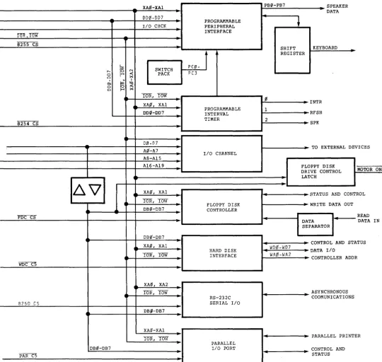
Figure 3-8
I/O Interface Diagram
XA0-XAI PB(1-PB7 SPEAKER
DATA
000-007 PROGRAMMABLE
1/0 CHCK PERIPHERAL
m. T"Q"W0 INTERFACE 8255 CS
SHIFT KEYBOARD ~
REGISTER
\8 SWITCH
PC0-t-- N
PC3 0 <t: PACK
0 :><
I
~
I(So. lSI
0 <t: 0 :><
lOR, lOW
~ INTR
XA~, XAI
PROGRAMMABLE 1
DD(.J-DD7 INTERVAL RFSH
TIMER 2
8254 CS SPK
D0-07
TO EXTERNAL DEVICES
Art-A7 1/0
CHANNEL A8-A15
A16-A19 FLOPPY DISK
MOTOR ON DRIVE CONTROL
LATCH
~\l
XA~, XAI STATUS AND CONTROLlOR, lOW
FLOPPY DISK WRITE DATA OUT
DB0-DB7 CONTROLLER
FDC CS READ
DATA DATA IN
SEPARATOR DBrt-DB7
CONTROL AND STATUS
XA0, XAI WD0-WD7
DATA 1/0
HARD DISK
lOR, lOW INTERFACE W,ll,0-WA2
CONTROLLER ADDR WOC C5
XA0, XA2
lOR, lOW ASYNCHRONOUS
RS-232C COOMUNICATIONS
8250 CS SERIAL 1/0
DB~-DB7
XA~-XAI
TS 1605/1605B Technical Reference Circuits
Table 3-3 lists the major component of the serial I/O and its description.
Table 3-3 I/O Component
Device or Line
Serial I/O Controller
Source/Description
An RS-232Cdevice thatis usedfor
asynchronous communications only, but is
capable of supporting current loop operation. Enabled by CPU lines XAO through XA2 and DBO through DB7 and control signals -lOR, -lOW,
and -8250 CS. This device can be programmed
from 50 baud to 9600 baud.
PARALLEL PRINTER PORT
The parallel port is a general purpose I/O port configured on the
TS 1605/l605H to interface to a parallel printer. Interrupts can
be enabled or disabled under program control. Since a 25-pin,
0-type connector is used in this system, a special cable is required for interface to a standard Centronics-type printer. See Figure 3-9 for a diagram of the parallel printer port.
U8 is a bidirectional receiver with the direction controlled by the parallel chip select or an I/O read.
Write data in U6 is read back through UIO. Then write control
and write information goes into INIT, SLST N, AUTO FD XT, STROBE.
Read control is enabled to read those control signals. Once
read, the system and hardware are functioning properly. Then status is read from the printer for error, busy, ACK, PE, or
select. Then write data is sent to the printer. STROBE then
goes to low. This initiates read status to read busy and ACK
signals from the printer. When okay, reads information into the
CPU via the data bus. Then a write data into U6, then strobe
data with write control signal into parallel printer. Then
another read status cycle. This process continues until all of
the data is transferred.
NOTE! Read control is performed for the data latch only when
the system is first booted up.
~
D~1\
..
74LS245..
r
- D7
J U13 DB~ - DB7
..
..
~DIR
PAR RD ... U89
AAAAA
74LS155 C""""" '" '" '" "'-+5U
XA~ 13 A 7 READ DATA lYO
XAI 3 lYl 6 READ CONTROL
1
B U202
IG .2...READ STATUS
)U97 lY2
PAiiCS 9 WRITE
T
14 2G 2YO DATAI
15 11 WRITE
lOW
2C 2Y2 CONTROL
U29
3BD
-P2-25 ERROR
tL
1 DB3
OEA P2-11> BUSY
ACK DB~ - DB7
P2-10 ...
-
U12P2-12) PE
~
SLCT
P2-13~ 74LS240
SLCT IN
INIT ....
~
74LS374..
~ ".~..
U6
3BC f CK 74LS244 ~
..
~..
l -t:O0 U18
11G I
"& 3BC
-
t:O0
3BE
lCK
i'... DB~ 74LS374
V ~_ DBI
V
DB2
\
~1>""
DB3..
...
DB4DB4 U!l
~,
~ P2- 2
DATA~ - DATA7 ) : -
..
P2- 9All I \ .... 2G STROBE
-AUTO FD XT
-INIT
-SLCT IN
--IRQ ENABLE
P2-1
P2-14
P2-16
P2-17
togt;2
PI ....
"''-0
PIC 1-1 ...
I-ItD tD I-IW I tog\G
...
....
::s rt tD...
~ 0'-0
....
TS 1605/16058 Technical Reference Circuits
The major parallel
U6 UIO U12 U9 U20
The major parallel
Table 3-4
Major Parallel I/O
Device or Line
Data Latch
Data Buffer
Status Buffer
Control Latch
KEYBOARD INTERFACE
IIO components are:
Data Latch Data Buffer Status Buffer Control Latch Multiplexer
IIO components are in Table 3-4.
Components
Source/Description
Used as a temporary storage buffer for data transmitted to the parallel printer on output
lines DATAO through DATA7. Data is written
into the data latch by the CPU when signals -PAR CS and -lOW are activated. Data lines DBO through DB7 carry data transfers to this
latch.
Buffers output lines DATAO through DATA7 into data lines DBO through DB7.
Buffers status signals, -ERROR, SLCT, PE,
-ACK, and BUSY that go from the parallel
printer to the CPU. These signals are read by
the CPU when -lOR and -PAR CS are activated.
Control signals -STROBE, -AUTO FEED, -INIT, and -SLCT IN are transmitted to the parallel printer when the CPU enables lines -lOW and -PAR CS.
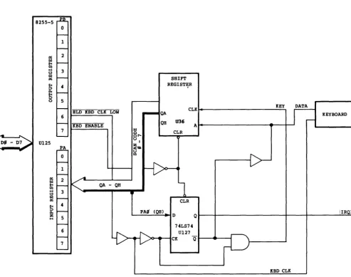
The TeleVideo and IBM keyboards are not plug-compatible. A TeleVideo keyboard must be used with the TeleVideo system.
Under normal keyboard conditions, the output register of 8255, PB bits 6 and 7, control the keyboard-enabling circuit - bit 6 is
high, bit 7 is low. In this condition, the keyboard circuit can
receive data from the keyboard. Whenever the key is pressed, the
data goes from the keyboard to input A of the Ul16 input register
(see Figure 3-10). At the same time, the keyboard clock sends
information through inverter U19 and through AND gate U25 and
then to the clock of the shift register. This clocks the 8-bit
code representing the number of the key that was pressed. The
start bit is the MSB (QH). When the information is stored in the
shift register, QH is fed back to the data input of D flip-flop
U127. When the clock goes in, it generates interrupt IRQ1. This
sends the microprocessor into the interrupt service routine which processes the key.
TS 1605/1605B Technical Reference Circuits
When the interrupt is generated at the Q output with a logic
high, the Q is a logic 0 which is sent back to the keyboard data input via U7 and that prevents the keyboard from sending more
data. It also inhibits U25 to prevent the keyboard clock from
shifting more data into the shift register.
Figure 3-10
Keyboard Circuit
8255-5 ~
0
r
-1
l "
-ll:: 2
1&1 r
-Eo<
til
~
3
(.!)
1&1 r -Il::
Eo< 4
0
Po r
-Eo<
0
0 5
t
-SBIFT REGISTFtR
CLK KEY DATA
BLD KBD CLK LOW
I
, - -OA KEYBOARD
6
r
-OB 036
t - - KBD ENABLE A
7 1&1
CLR
~
" - - - §"Dlf - D7 U125 u.
~ ~\Sl
..
U0 til
r
-~
1 I "
-~
Il:: 2 1&1
1
Eo< r - OA - OB
til
~ 3
(.!)
1&1 r
-Il:: CLR
Eo< 4
0 t
-PA~ COB) iIROl
Po
z 5 D 0
~
t - - 74LS74
6
lCrrl>
U127t - - CK 0"
7
~
TS 1605/1605B Technical Reference Circuits
The major components of the keyboard interface are:
U37
U38
Intel 8255A-5 Programmable Peripheral Interface (PPI)
Serial Shift Register
The major components of the keyboard interface and their description are listed in Table 3-5.
Table 3-5
Keyboard Interface Components
Device or Line
Programmable
Peripheral Device
PAO-PA7, PBO-PB7, PCO-PC7
AO-AI
Serial Shift Register
Source/Description
Programmedby system software, this device reads the eight-position DIP switch and interfaces to keyboard receiving and
transmitting scan code. Controls audio
speaker tone and enable/disable I/O channel
error check. Enabled by address lines XAO
through XAI, data lines DDO through DD7, and control signals -lOR, -lOW, and -8255 CS.
PPI. Ports A, B, andC. Each port is
composedof eightbits, configured by system software. Accepts commands from read/write control logic, receives control words from the internal data bus, and issues the proper commands to the associated ports.
Cpu. Port select input signals, in
conjunction with -RD and -WR signals, control the selection of one of three ports or the control word registers.
Permits complete control over incomingdata
lines PAO through PA7. Data at serial inputs
may be changed while clock is high or low, but only information meeting set-up
requirements is entered. Clocking occurs in low-to-high transition of clock input.
SPEAKER DRIVE SYSTEM
You can control the frequency of the speaker output by
programming the different frequencies coming from timer 8254 (see
Figure 3-11). The speaker frequency is controlled by the
frequency divider in the 8254 timer 2. The frequency can be
controlled by programming so you can change it through software. Bit 0 of the output register PB of the 8255 is used to control the speaker gate so you can turn the timer on and off. The timer
clock is ANDed with the 8255 output register PB bit 1. The
output of U26 provides the information to speaker drive Q25.
TS 1605/1605B Technical Reference Circuits
The speaker driver is controlled by 8255. 0 enables the speaker
interface. Channel 2 timer clock is used to supply the oscillating frequency to control the speaker.
When you want to turn on a speaker, use 8255 PB 1.
8255 PPI
U37
PB 0
1
2
6
7
8254 CLK
SPEAKER GATE
SPEAKER DATA
TYPE 8 INTERRUPT
TO 8088
U27
8254 TIMER
TIMER CLOCK
GATE 2
01
SPKR DRIVE (PBa)
(PBI)
en~
"0 ....
tD~
AlC
~..,
tDtD
..,
W
c;,1
.., ....
...
<I
tD en
~
en
rT
tD
IS
t-3
en
....
G\
C)
U1
""
....
G\
C)
U1
=
t-3
tD
n ::r
::I
....
n AI
....
~
tD t-h tD
..,
tD
::I
n
tD
n
....
..,
n
C
....
rT
TS 1605/1605H Technical Reference Circuits
INPUT/OUTPUT CHANNEL
The input/output channel, located on the system board, provides
interface to I/O devices external to the system board. This
channel consists of a connector with data and address buses, control signals, interrupt lines, DMA control lines, and power
and ground lines. The I/O channel pin configuration is listed in
Appendix F. A block diagram of the input/output channel is shown in Figure 3-8.
FLOPPY DISK CONTROLLER
The floppy disk control circuitry is based around the 8272A (U96)
floppy disk controller chip. The 9229B FDe does all write
precompensation functions. The 8272A keeps track of where the floppy heads are currently located and stores more internal memory than previous floppy disk controllers. Also, data being read from the disk is intercepted by a 9229B (U81) Data
Separator. The Data and Clock pulses that compose MFM data on
the diskette are separated and synchronized with the 8272A
internal clock to ensure accurate data exchanges. The 8272A FDe
is programmed to operate in the burst transfer mode at system initialization by the EPROM.
The other important support Ies are the bidirectional buffer
(U13) and the floppy disk latch (U42). They control the
selection of the disk drive and the turning on of the floppy
motor. These are taken as control words from the system data
bus.
The basic functions of the floppy disk controller circuitry are 1) writing data to the diskette, 2) reading data form the
diskette 3) determining where to write on the diskette, and 4)
turning the drive off and on and selecting drive A or B. 1, 2,
~ tD
...
tD<
....
C. tD o fn'< en
rt tD IS en ... H ::s n •
:
\Q tD W • ~ G\ r"I
16 MBZH
~
TIMINGosc.
2
.
WRITE 03 PRECOMP.DATA SEPARATION
~ DATA BOS
~ BOFFER f----.,...
_ _ ...;0..;,8_ ...
rY.
DB7 A ,,~
~
.---READ DATA WRITE DATA I I 1 I I1 _ _
-J
j
f'PT SENSOR WRITE G~~~~ SIDE SELECT <....
Ir=>
READ/ WRITE AMPLIFIERHEAD READ
FILE PROTECT SENSOR (WRITE PROTECT) HEAD WRITE
I
iC-.FILE PROTECT SENSOR
INDI-CA,\R ~ FILE PROTECT SENSOR LED
r---;::P~S-9-,R-W--... ~ PS1,RDD
CLK,MFM WCB,WD
WRITE GATE J
WRITE DATA, ~ ERASE GATE
INDICATOR
I / ~~INDF.X SENSOR LED
n
I
t>~'~'
r - : : : : X SENSORL _ _ _ _ _ .I FRONT PANEL LED II ,/ ",:,XS:. 0-...':, or SPINDLE MOTOR
-
INDEX ::::: TRACK nil... ~
WRITE PROTECT '" ~ DBB - DB7
0,...--... '1 HEAD SELECT
al
~
~
DIRECTION DRIVE SELECT If
r
STEP
~
f:;
al
FDC 8272 v
MOTOR ON
v
07
I
L ..
~ LT~IL---.,
l . . . ,
I
- " eo"
"'~ ,=~" ~
---~,~ ~~
• 024 I- 034
,m,,,,,
~'"''''
_ ""
r
~~~"-<..<Et--FLOPPY DISK DRIVE
1
I
I
1
I
POWER SENSE READ DATA
MFD CONTROL 5V OV I~-""'" 1 I I I 1 I I
MOTOR ON
PHASE CONTROL TRACK «« SENSOR HEAD LOAD SOLENOID INDEX SENSOR INDEX SENSOR LED F' .F. PIlOTE:T SENSOR .ED
(DRIVE SELECT)
'----'==-.;..:~::.::.::..:---+-+----I 1
\0
~l~-=-~~::, ~;, {){!~'>6:~r
MAGNETIC BEAD BEAD LOAD SOLENOID
TRACK Oil SENSOR
STEPPING MOTOR I
FLOPPY DISK CONTROLLER CIRCUIT
TS l605/l605H Technical Reference Circuits
The major components of the floppy disk controller are:
U96 U42 U8l
Intel 8272A Floppy Disk Controller Device Floppy Disk Drive Control Latch
FDC9229B Data Separator
The floppy disk controller components and their description are listed in Table 3-6.
Table 3-6
Floppy Disk Controller Components
Device or Line
Floppy Disk Controller
-COMP READ DATA
-COMP WR DATA
Floppy Disk Drive Control Latch
Data Separator
Source/Description
Pr