ABSTRACT
CHANG, TZU-HSUAN. In-situ Scanning Electron Microscopy Mechanical Characterization of Crystalline Nanowires using MEMS Devices. (Under the direction of Dr. Yong Zhu).
The nanostructures such as nanoparticles, nanowires (NWs), nanotubes and graphene are important building blocks for a broad spectrum of nanotechnology applications including energy harvesting and storage, nanoelectromechanical systems (NEMS), flexible electronics and stretchable electronics, where the ultrahigh strength is of direct relevance. Therefore, it is of important to accurately characterize their mechanical response. Microelectromechanical systems (MEMS) is the reliable platform while performing the in-situ characterization of nanostructure. It can measure not only the mechanical properties of nanomaterials but also other significant physical properties such as electrical or thermomechanical. In this thesis, we conduct the MEMS tensile stage to study the mechanical behaviors of two important NWs: Si NWs and Ag NWs.
We start with an overall review on recent advances in experimental techniques conducting MEMS devices for nano-mechanical testing. Such platforms have been used for basic tensile testing, fatigue, thermomechanical testing, multiphysical testing, and true displacement-controlled testing via feedback control. A large number of nanostructures have been characterized including carbon nanotubes, crystalline NWs, metallic glass NWs, and polymer nanofibers.
ambiguous results on either brittle or ductile failure of Si NWs are found, which are going to be clarified in this report. A novel temperature controllable MEMS tensile platform for NWs characterization is therefore designed and carefully calibrated. Multiphysics finite element analysis (coupled electrical-thermal-mechanical) was carried out to optimize the structure design and minimize undesired thermal displacement during heating. The simulation results of temperature distribution on MEMS device are confirmed by the in-situ Raman spectroscopy. The Si NW clamped on the MEMS tensile platform is able to be heated up close to 600 K.
Using this device, we thoroughly study the thermomechancical properties of Si NWs. Both Young’s modulus and fracture strength of the Si NWs decrease with the increasing of the temperature. In addition to the experimental finding, a new approach in order to assess the BDT of crystalline Si NWs is proposed in this report. The activation volumes of dislocation in crystalline Si NWs acquired from in-situ SEM tensile testing and thermal activation analytical model show a clear deformation mechanism transition. The dislocation nucleation induced shear band and diameter reduction were confirmed by TEM postmortem imaging which strongly support that the Si NWs were undergoing plastic deformation at temperature of 600 K.
In-situ Scanning Electron Microscopy Mechanical Characterization of Crystalline Nanowires using MEMS Devices
by
Tzu-Hsuan Chang
A dissertation submitted to the Graduate Faculty of North Carolina State University
in partial fulfillment of the requirements for the degree of
Doctor of Philosophy
Mechanical Engineering
Raleigh, North Carolina 2016
APPROVED BY:
_______________________________ _______________________________
Dr. Yong Zhu Dr. Chih-Hao Chang
Committee Chair
_______________________________ _______________________________
DEDICATION
BIOGRAPHY
Tzu-Hsuan was born in Taipei, a city in northern Taiwan. It is the capital, economic center and the largest city of Taiwan. He received his B.S. degree in Civil Engineering on 2007 from National Taiwan University, which is ranked as the No.1 university in Taiwan. He continued his study as a master student in Civil Engineering at National Taiwan University and graduated on 2009 under the advisory from Dr. Chuin-Shan Chen and co-advisory from Dr. Long-Sun Huang at Institute of Applied Mechanics. During his master study, he measured and characterized the alkanethiols absorption behaviors on a gold-coated MEMS cantilever. After finishing the mandatory military service as Taiwanese citizenship, he started his PhD program at NC State under the advisory of Dr. Yong Zhu in August 2012. His PhD research focuses on the mechanical properties characterization of crystalline nanowires.
ACKNOWLEDGMENTS
First of all, I would like to thank my advisor Dr. Yong Zhu who leads me into the fascinating field of the nanomaterials and related technologies and have been always there to share with his knowledge and help with all aspects of my study. It has been an invaluable experience for me to learn and work with him. This work could never be done without his guidance and encouragement.
Many appreciation to my committee members, Dr. Chih-Hao Chang, Dr. Mark Pankow and Dr. Joseph Tracy for their effort on keeping providing precious suggestions and critical questions to make this work more fulfilled during the time of preliminary exam and final oral.
I am deeply thankful of help and friendships of my fellow group mates, both the current and former members of the Zhu group. I would especially like to recognize Guangming Cheng, who has been worked with me on the nanowire manipulation and in-situ experiments since the beginning. All the TEM images showed in this thesis are taken with his help. I am also grateful for the time Qingquan Qin was in the group, as he was one of the first students of Zhu group and helped me a lot when I joined. Other members, post-doc fellows Tao Jiang, Alper Gürarslan and Qijin Huang; senior PhD student Shanshan Yao; younger students Zheng Cui, Jianxun Cui, Chengjun Li and Felipe Poblete, it is a great pleasure to share many good times and bad times with you guys.
I would like to thank my master thesis advisor Dr. Chuin-Shan Chen at National Taiwan University for encouraging me to go to the US and sharing his experience when I got lost. I am also truly grateful for the friendships with my roommates, Chian-Ting Tang and Wei-Ting Chen. It was a wonderful moment to share time with you guys on baseball court in many weekends outside of the work.
Last but not the least, I want to express my appreciation and love for my family in Taiwan, especially my mom and wife who spent lots of time on phone to encourage me when I felt frustrated. I could never have accomplished this without their support.
TABLE OF CONTENTS
LIST OF TABLES ... ix
LIST OF FIGURES ... x
Chapter 1. Introduction ... 1
1.1. Silicon nanowires ... 3
1.1.1. Synthesis ... 4
1.1.2. Mechanical characterization ... 7
1.2. Silver nanowires... 9
1.2.1. Synthesis ... 9
1.2.2. Mechanical characterization ... 12
1.3. Thesis outline ... 15
Chapter 2. Review of Microelectromechanical Systems for Nanoscale Mechanical Characterization ... 16
2.1. MEMS tensile testing platform: Actuator and sensor ... 17
2.2. Sample preparation ... 22
2.3. Displacement/strain measurement ... 24
2.4. MEMS device configurations ... 26
2.5. Platforms for Multiphysical Testing ... 32
Chapter 3. A Microelectromechanical System for Thermomechanical Testing of
Nanostructures ... 38
3.1. Introduction ... 38
3.2. MEMS tensile stage for thermomechanical testing of nanostructures ... 40
3.3. In-situ tensile testing of SC silicon nanowire ... 49
3.4. Summary ... 50
Chapter 4. Temperature Effect on Mechanical Properties of Silicon Nanowires ... 52
4.1. Introduction ... 52
4.2. Brittle-to-ductile transition of silicon... 53
4.2.1. BDT of bulk silicon ... 54
4.2.2. BDT of silicon at micro/nano scale ... 61
4.2.3. Conclusion ... 70
4.3. Brittle-to-ductile transition of bi-crystalline Si NWs... 74
4.3.1. Experimental section ... 74
4.3.2. Results and discussion ... 76
4.3.3. Summary ... 89
Chapter 5. On the Size-Dependent Elasticity of Penta-Twinned Silver Nanowires .. 91
5.1. Introduction ... 91
5.2. Materials and methods ... 94
5.3. Results and discussion ... 97
Chapter 6. Conclusion and Future Work ... 109
6.1. Conclusion ... 109
6.2. Future work and outlook ... 112
REFERENCES ... 114
APPENDICES ... 147
APPENDIX A. Derivation of the formula for the evaluation of thermal activation process ... 148
APPENDIX B. Error analysis of Young’s modulus ... 149
LIST OF TABLES
Table 2-1 Summary of MEMS platforms for tensile testing of 1D nanostructures. ... 37
Table 3-1 Material parameters used in the simulations ... 44
LIST OF FIGURES
Figure 1-1 (a) Illustration of Si NW-based thin film transistor on a plastic substrate [22]. (b) Schematic illustrating the conversion of NW-based FET into a pH sensor [26]. ... 4
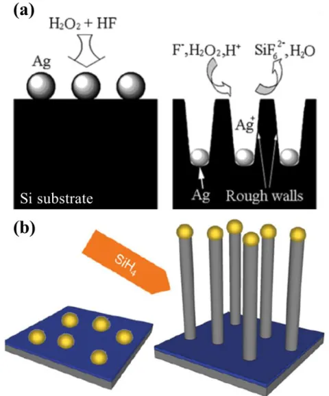
Figure 1-2 Schematic elucidations of the formation mechanism of SiNWs arrays via: (a) metal-assisted chemical etching [29]; (b) VLS growth [20]. ... 6
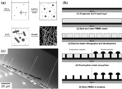
Figure 1-3 (a) Schematic drawing of the process that synthesis silver nanowires via a Pt-seeded polyol method [44]. (b) Schematic illustration of the fabrication process for metal nanowires through membrane-based synthesis [50]. (c) SEM image of Cu nanowires grown on the Si substrate [51]. ... 11
Figure 1-4 Stress-strain curve for penta-twinned Ag NWs: (a) For various diameters. Inset shows the microstructure of penta-twinned built by MD simulation [66]. (b) During loading, relaxation, unloading and recovery [55]. ... 14
Figure 2-1 Schematics of common in-plane mechanical actuators. (a) Comb drive actuator, (b) V-shaped thermal actuator, (c) Z-shaped thermal actuator. The black and grey colors represent anchors and moveable parts, respectively. ... 20
Figure 2-3 (a) The MEMS platform consisting of a loadcell, actuated by an external actuator for nanofiber testing [140]. (b) DIC displacement measurement [136]. (c) The push-to-pull MEMS platform by Haque and co-workers. An external piezo actuator pushes from the left side [135]. ... 30
Figure 2-4 A MEMS platform including a thermal actuator (a) or comb drive actuator (b), a capacitive load sensor and a specimen in between (fabricated by Poly-MUMPs) [89]. (c) A platform consisting of a thermal actuator, a specimen gap, and a capacitive load sensor (fabricated by SOI-MUMPs) [142]. (d) A platform including a comb drive actuator and a beam load sensor [111]. Inset shows a magnified view of the three-beam structure, which is attached to the device in the boxed area. ... 32
Figure 2-5 (a) Schematic of the vacuum cryostat system for temperature control [143]. (b) Schematic of a MEMS thermomechanical platform made of SiC including a co-fabricated temperature sensor [144]... 34
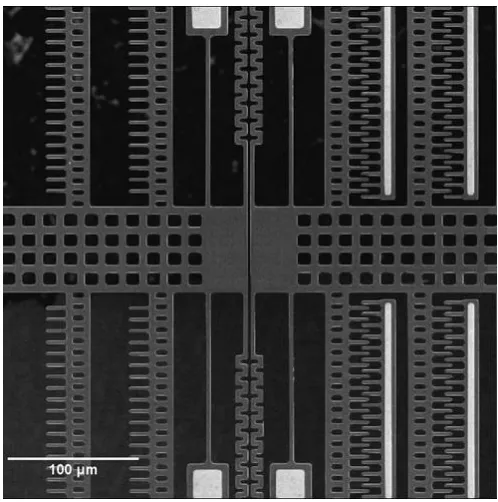
Figure 3-1 (a) SEM image of the entire MEMS device that consists of three parts: comb drive actuator, capacitive load sensor and heater. (b) Magnified view of the heater as boxed in (a). The arrows indicate the current direction. ... 40
Figure 3-2 SEM image showing the fabricated MEMS thermomechanical testing device that has a serpentine heating coil that can be resistively heated. ... 42
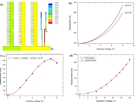
Figure 3-3 (a) Simulated temperature distribution under 4 volt heating voltage in vacuum, (b) simulated temperature profile at points A and B as functions of heating voltage, (c) measured thermal displacement as a function of heating voltage, (d) displacement of comb drive actuator as a function of actuation voltage at room temperature (theoretical calculation according to Eq. (3-1)) ... 45
Figure 3-4 (a) Simulated temperature distribution under 4 volt heating voltage in air, (b) temperatures profile at points A and B as functions of heating voltage in air. ... 47
Figure 3-5 (a) Temperature contour of MEMS device and mounted nanowire. (b) Raman spectra of point B and C under 8 V heating voltage in air. ... 48
Figure 4-1 Schematic drawing of single crystalline Si specimens for BDT testing, (a) tapered-double-cantilever-beam, and (b) four-points-bending. ... 56
Figure 4-2 Stress intensity factor (K) versus temperature; black dot line represents brittle cleavage; red solid line represents brittle-to-ductile transition region; blue dash line represents ductile failure. ... 59
Figure 4-3 (a) Force-displacement curves in AFM bending tests for NWs with 200 nm in width at elevated temperature [200]. (b) Force-displacement curves of single crystalline silicon beam with different sample size [167]. (c) SEM images of plastic deformation of single crystalline silicon under bending. ... 62
Figure 4-4 (a) Illustration of the single crystalline silicon sample with single edge notched. (b) SEM and TEM image of single crystalline silicon sample fracture at 300 °C. ... 64
Figure 4-5 (a) A series of TEM images show severe plastic deformation of a single crystalline Si NW under tensile stress. (b) Stress-strain response of a single crystalline Si NW with diameter of 23 nm under repeated loading and unloading. Inset shows a SEM image of the broken end of the Si NW... 66
Figure 4-7 Plot of temperature versus sample size [12], [38], [142], [161], [169], [170], [186], [187], [196], [200], [167], [202]–[206], [208], [214], [222]. The open symbols represent a ductile deformation while the solid symbols represent only brittle failure. ... 70
Figure 4-8 (a) SEM image of a Si NW attached to the lacey carbon TEM grid. The nanomanipulator was trying to approach the Si NW from the underneath to lift it off. (b) The corresponding HRTEM image and SAED pattern of the red squared area in Figure (a), showing bi-crystalline structure, which consist of two {111} planes with growth direction of <112>. (c) The Si NW was lifting off from the lacey carbon grid by the nanomanipulator. (d) SEM image of the Si NW across the actuator and sensor. Two white arrows indicate the EBID-Pt strain marker. ... 75
Figure 4-9 Stress-strain response of the Si NWs (a) with diameter of 60 nm under repeated loading and unloading at room temperature, (b) with diameter of 58 nm at elevated temperature. ... 78
Figure 4-10 (a) Measured Young’s modulus of crystalline Si as a function of temperature. (b) The binding energy between atoms as a function of inter-atomic distance, replot from DoITPoMS, University of Cambridge. ... 81
Figure 4-12 TEM postmortem images showing crack behavior of Si NWs with similar diameters failed at different temperature, (a) room temperature and 105 nm in diameter; (b) 564 K and 107 nm in diameter. ... 88
Figure 5-1 (a) SEM image of a penta-twinned Ag NW with one end welded on the tip of the tungsten probe. (b) SEM image of the same penta-twinned Ag NW under resonance. (c) SEM image of the MEMS testing stage with the same penta-twinned Ag NW. Inset shows the NW across the actuator and load sensor. The two small arrows indicate the deposited strain markers. Scale bar, 500 nm. ... 96
Figure 5-2 A series of SEM images showing the process of transferring penta-twinned Ag NW. (a) Use the second probe to approach the NW that attached on the first probe. (b) Detach the NW from the fixed end of the first probe. ... 97
Figure 5-3 (a) The amplitude versus frequency plot of a penta-twinned Ag NW with diameter of 62 nm. (b) Stress-strain of the same penta-twinned Ag NW under tensile loading. ... 98
Figure 5-4 (a) Apparent Young’s modulus as a function of NW diameter without any cross-sectional shape modification. (b) Modified Young’s modulus as a function of NW diameter. The measured Young’s modulus was normalized by the bulk modulus of 84 GPa. The tension data using AFM cantilever (in blue open triangle) were reported in a previous paper [64]. ... 100
Figure 5-6 Summary of the elastic modulus obtained by experiments and simulations [60], [61], [65], [247]–[249], [251], [255]. The dashed line represents the Young’s modulus of bulk Ag... 104
Figure 5-7 Young’s modulus as a function of NW diameter for those NWs on which both resonance and tension tests were performed. ... 105
Chapter 1.
Introduction
Recent advance in nanotechnology has brought forth a host of nanostructures, such as nanoparticles, nanowires (NWs), nanotubes and graphene that exhibit ultrahigh mechanical strength (e.g., sample-wide stress > 1/10 of their ideal strengths) [1]. Such nanostructures are important building blocks for a broad spectrum of nanotechnology applications including energy harvesting and storage [2–4], nanoelectromechanical systems (NEMS) [5,6], flexible electronics [7,8] and stretchable electronics [9–11], where the ultrahigh strength is of direct relevance. It is known that electronic band gaps change with elastic strain, so do phononic band gaps, thermal transport and other physical and chemical properties. Therefore, the ultrahigh strength offers unprecedented opportunities to tune the functional properties of nanostructures through the elastic strain engineering [1]. As an example, Si NWs were found to exhibit an enormous range of elastic strain (e.g., > 10%) [12], which is promising for future semiconductor engineering such as field effect transistor built via Si NW arrays [13,14].
nanoscale mechanical behavior from both computational and experimental perspectives. Indeed, recent rapid advance in nanoscale manipulation/mechanical testing [17,18] and in-situ characterization tools such as electron microscopies [19,20] has enabled real-time observation of deformation and defect dynamics. As the number of atoms in these nanostructures comes increasingly within the reach of the state-of-the-art computational modeling capabilities, direct comparison between nano-mechanical tests and atomistic simulations side by side has become closer to reality and hold great promises for important new discoveries in materials science.
Among these, Si NWs and Ag NWs are two of the most applied nanomaterials since they can be massively produced with high quality and are mechanically, electrically and thermally outstanding [21,22]. For Si NWs, clear evidences of enhancement on mechanical behavior have been reported by various approaches [12,23–25]. In contrary, the thermal-mechanical response of Si NWs still remains inconsistency due to the experimental difficulty in performing in-situ mechanical testing with various temperatures for such small specimens. One particular interest from engineering view is the temperature range for triggering brittle to ductile transition (BDT) of Si NWs. It is of important because Si NWs have been considered as the building blocks of future NEMs sensors and anodes for Li battery [3] where high temperature will be often involved.
research and application aspect. For the studies on mechanical response, increased Young’s modulus and yield strength with decreasing NW diameter have been recently discovered via tension [29,30] and bending [31,32]. However, the elasticity size effect of penta-twinned Ag NWs was found to be more pronounced under bending than tension and resulted in ambiguous conclusions in literatures. Understanding the origin of size effect will not only provide the guidance for the application design but also help to probe the fundamental physics.
Therefore, in this thesis, we are going to address these important mechanical issues mentioned above of Si NWs and Ag NWs. For Si NWs, we developed an integrated MEMS platform that can perform mechanical testing with various temperatures inside a SEM and combined in-situ tensile testing with ex-situ TEM observation of dislocation activities to unveil the BDT of Si NWs. For the Ag NWs, we conducted two independent experiments on the same NW, in-situ resonance test and tensile test in a SEM, to measure the Young’s moduli in order to compare the difference under different loading mode and solve the discrepancy in the literatures.
1.1. Silicon nanowires
oscillators [5], mechanical sensor [34], field effect transistors (Figure 1-1(a)) [35,36], photovoltaics [37] and lithium batteries [3,38]. In addition, because of the extremely high surface to volume ratio combined with excellent ion sensitivity, Si NWs became a great candidate of chemical and biochemical sensors as well (Figure 1-1(b))[14].
Figure 1-1 (a) Illustration of Si NW-based thin film transistor on a plastic substrate [35]. (b) Schematic illustrating the conversion of NW-based FET into a pH sensor [14].
1.1.1. Synthesis
Numbers of synthesis techniques nowadays exist to fabricate Si NWs. In general, these can be classified into bottom-up and top-down methods. The top-down approach usually involves in lithography, etching, and deposition, which utilize to pattern bulk materials to small scale. One of the most attraction ways to prepare large area arrays of nanowires via etching-based of top-down strategy was demonstrated by Zhu and co-workers [39,40], and extensively developed by others later [41,42]. The way of fabrication is based on
induced excessive local oxidation and dissolution of a silicon wafer substrate in HF/Fe(NO3)3
solution. Such method was utilized previously to prepare porous silicon. Details of fabrication are schematically shown in Figure 1-2(a). First of all, Si wafer was electroless deposit silver (Ag) nanoparticle layer. The distribution of Ag particles on the Si surface determines the density and size of the Si NWs after etching. The Si wafer covered by Ag particles is then immersed in an aqueous HF/Fe(NO3)3 solution at 50 °C. In general, the
etching process of normal Si wafer in HF/Fe(NO3)3 is very time consuming. But with the
Figure 1-2 Schematic elucidations of the formation mechanism of SiNWs arrays via: (a) metal-assisted chemical etching [41]; (b) VLS growth [33].
to millimeter [47]. VLS synthesis requires a catalyst on the grown substrate, which usually were liquid gold (Au) nanoclusters. Then the target material compound (i.e. SiH4 for Si NWs
[48]) is introduced in gas phase to saturate nanoclusters. Once reaching supersaturation, the nanocluster started displaced from the surface of the substrate and sat on the top of growing nanowires, as illustrated in Figure 1-2(b). The nanowire diameter is mainly determined by the size of nanocluster and the length can be simply tuned by controlling the exposure time.
1.1.2. Mechanical characterization
Silicon NWs so far is one of the most studied semiconductor materials since it is the fundamental building block for nanoelectronic and nanoelectromechanical devices. A particular concern is the size effect on mechanical properties, such as Young’s modulus, failure strain and stress, which highly affect the reliability and performance of device. One predicament scientists have encountered was uncertain growth direction of the NWs and hard to characterize before test. They could be randomly grown along either [100], [110], [111], or [112]-oriented even using the same synthesis method on the same substrate [48–50]. Anisotropic material properties further increased the difficulty for researchers to interpret the equivocation in nano-scale.
bulk value while the diameters of NWs are below 30 nm, and the smallest value was around 80 GPa. Meanwhile, the elastic strain of NW was keeping increase and could sustain fracture strain as high as 12%. Although the authors did not characterize the growth direction for every NWs in the report, compare to bulk value, the softening in the Young’s modulus of Si NWs is clear no matter what the growth direction is. The results are most likely due to the surface effect, which was correlated with the surface reconstruction that lead to bond saturation, bond contraction or elongation, and loss of bonding neighbors.
Steighner et al. developed a method to pick and mechanical test a single NW with desired orientation [51]. The NWs were first placed on the lacey carbon TEM grid and the growth orientation was defined by TEM. The chosen NW was then picked up from grid and transfer to a MEMS tensile test stage inside SEM by pick and place method. They test seven NWs with diameters range from 268 to 840 nm, and three different growth direction, which are [110], [111], and [112]. A similar size dependent strength was found in these NWs. In addition, the growth direction dependent strength has been discovered as well. The failure stress and strain increased with the decrease of NW diameters, while [112]-oriented NWs possessed the highest failure strain and stress, followed by [110], and the smallest one is [111]. Besides, in both reports, all of the stress-strain behavior showed only linear without potential plastic deformation.
in-situ test nanowires with elevated temperature is still a challenge. In Chapter 3, we design a temperature controllable MEMS device which is able to perform in-situ SEM/TEM material characterization. In Chapter 4, we will first briefly review the current studies on the BDT of single crystalline silicon, and then conduct in-situ tensile testing to unveil thermomechanical properties of single crystalline Si NWs using the MEMS device we fabricated in Chapter 3.
1.2. Silver nanowires
Face-center-cubic (FCC) metal NWs, including gold, silver and copper play especially important role in the field of stretchable and flexible electronics due to their extraordinary electrical conductivity and mechanical ductility [11]. Among all these materials, silver has the highest conductivity. As such, Ag NWs became the most extensively studied and utilized metal nanostructures as conductors. In addition to its advantage on electrical conductivity, Ag NWs also possess a noticeable surface plasmon resonance property [52,53], which makes them become the great candidate of biosensor [54] and plasmonic waveguiding [55].
1.2.1. Synthesis
with ethylene glycol (EG) heated to 160 °C. The reason of forming a decahedra shape is due to the most thermodynamically stable seed, since it is bound entirely by the lower energy {111} facets [58]. These Ag/Pt nanoparticles could serve as seeds for the heterogeneous nucleation and growth of crystalline Ag NWs. Since the twin boundaries possess the highest energy on the surface of nanoparticles, silver atoms will tend to crystallize on those sites. As a result, the decahedra nanoparticle will elongate into a pentagonal nanowire with five-fold twinned grain boundary running along the length direction. The processes are illustrated in Figure 1-3(a).
Martin and co-workers developed a method called “template synthesis” for fabricating micro/nano structures via membrane-based synthesis [59]. This method involves synthesis of the nanostructures within the pores of a nanoporous membrane. Two types of membranes, track-etch polymeric and porous alumina membranes, are the most often carried out to fabricate nanostructures. The most advantage of this method is easy to synthesis various types of materials in addition to silver [60], including other metals [61,62], semiconductors, ceramics and organic polymers. Figure 1-3(b) illustrates an overall process to synthesis Cu nanopillars using PMMA layer as a template. The only restriction of sample selection is the desired material must be able to load into the pores based on vapor-phase sputtering, liquid-phase injection, or solution-liquid-phase chemical or electrochemical deposition.
deposited under ultra-high vacuum condition (<2
10-10 mbar) by molecular beam epitaxy. Substrate temperatures are controlled case by case for each material, e.g., 650 °C for cupper and 680 °C for gold. The deposition rate was set to be 0.05 nm/sec for all materials. Using this method, they have successfully grown high aspect ratio single crystalline nanowires of Cu [63], Au [65], Pd [64], Ag [67] and Au-Ag nanotubes [68]. Figure 1-3(c) shows a SEM image of single crystalline Cu nanowires grown on the Si substrate.Figure 1-3 (a) Schematic drawing of the process that synthesis silver nanowires via a Pt-seeded polyol method [57]. (b) Schematic illustration of the fabrication process for metal nanowires through membrane-based synthesis [62]. (c) SEM image of Cu nanowires grown on the Si substrate [63].
(a)
(c)
1.2.2. Mechanical characterization
The mechanical behavior of crystalline metals in small scale had received lots of interest over fifty years started from pioneering works which were done S. S. Brenner during 1950s [69–71]. Since then, numerous studies tried to approach by either tensile, compressed or bending experiments, and a few dedicated reviews had been published recently for experiments [15] and simulations [16].
In the field of nanoscale, the most well addressed material probably is penta-twinned Ag NWs since it is much more accessible with high quality and quantity than others. Early reports on mechanical testing of penta-twinned Ag NWs usually carried out an AFM-bending [32,31] test or nanoindentation [72,73] because they are easy to be manipulated. All of the above studies found a strong size dependent Young’s modulus in penta-twinned nanowires. For instance, for the NWs with large diameters (> 70nm), the Young’s modulus is close to the bulk value of 84 GPa. But the modulus increases with the decrease of size, which could be higher than 160 GPa. Recently, Zhu et al. [29] and Filleter et al. [30] reported the similar stiffening effect of increased Young’s modulus and yield strength with decreasing NW diameter. These NWs can sustain tensile stress as high as 2.64 GPa without apparent plastic deformation, which was close to the theoretical tensile strength of silver in the <110> direction based on the Schmid factor analysis of {111}/<112> system (3.5 GPa) [29].
hardening and multiple necking deformation mechanism via in-situ TEM observation [30]. With the assist of molecular dynamics (MD) simulations, they found out that the whole process was controlled by dislocation nucleation from a local stress concentrator, which leads to the formation of a linear chain of stacking fault decahedrons. Twin boundaries along the NW length can cause the formation of stacking fault decahedron chain and confine dislocation activities that locally harden the NW, resulting in enhanced flow stress and ductility. Narayanan et al. later reported a similar size dependent strain hardening effect through stress-strain relationship of both in-situ SEM tensile testing and MD simulation, as shown in Figure 1-4(a) [74].
between dislocations and existing twin boundaries during the relaxation step and the dislocation annihilation during the recovery step. Since the relaxation strain is rather small, a highly stable testing system (e.g. the MEMS platform used) is the key to observing such a fine behavior. Other testing systems such as those involving a nanomanipulator might not work due to the inevitable drift of the nanomanipulator. Similar recoverable plasticity on penta-twined Ag NWs has been reported in terms of athermal manifestation [75].
Although there is a general consensus regarding size effect elasticity of penta-twinned Ag NWs, the reported values were showing conflict in a certain degree. In Chapter 5, we will carefully address the discrepancy through a thorough literature review and cross-sectional TEM experiments.
Figure 1-4 Stress-strain curve for penta-twinned Ag NWs: (a) For various diameters. Inset shows the microstructure of penta-twinned built by MD simulation [74]. (b) During loading, relaxation, unloading and recovery [67].
1.3. Thesis outline
Chapter 2.
Review of Microelectromechanical Systems for Nanoscale Mechanical
Characterization
Characterizing mechanical properties of individual one-dimensional (1D) nanostructures is still challenging because of the following requirements: (1) constructing appropriate tools to manipulate, position and align specimens, (2) applying and measuring forces with nano-Newton resolution, and (3) measuring local deformation with nanometer resolution. Existing experimental methods for mechanical characterization of 1D nanostructures include vibration/resonance in scanning or transmission electron microscopes (SEM or TEM) [76– 80], bending using an atomic force microscope (AFM) in different operation modes [81–86], tension/bending/buckling in an SEM with the aid of a nanomanipulator [63,29,87–90] as well as nanoindentation [72,91]. Among all these methods tensile testing is the most straightforward one and it can measure a full spectrum of mechanical properties such as elasticity, plasticity and fracture.
such, MEMS have been employed in various nanotechnology-related applications ranging from nanomanufacturing [93] to cell manipulation [94]. Similarly, MEMS could have potential to impact the nanomechanical characterization through controlled actuation, high-resolution force/displacement measurements, integrated multi-functions and tiny size for in-situ electron microscopy testing. Zhu and Espinosa have developed an integrated nanoscale testing system using MEMS technology [95–98]. In the past decade, there has been extensive interest in developing MEMS-based instrumentation for experimental nanomechanics that will be reviewed in this article.
In this Chapter, we summarize the recent advances in the field of mechanical characterization of 1D nanostructures using MEMS platforms. We start with three commonly used device configurations and other design considerations such as actuation and load sensing mechanisms, device fabrication, sample preparation and displacement/strain measurement. After that, representative MEMS platforms are reviewed in accordance with the device configurations. Such platforms have been used for basic tensile testing, fatigue, thermomechanical testing, multiphysical testing, and true displacement-controlled testing via feedback control.
2.1. MEMS tensile testing platform: Actuator and sensor
(MTS) or screw-driven (Instron) actuator, a load cell (sensor), and a pair of grips. The same concept prevails at the small scale. There have been considerable efforts in developing instrumentation for micro/nano-scale tensile testing. However, the methods for actuation, sensing and even sample gripping are much different from the large-scale ones. In this section, we present brief review of utilizing MEMS devices as tensile testing platforms for 1D nanomaterials.
A number of actuation mechanisms have been implemented in MEMS including electrostatic actuation, thermal actuation, piezoelectric actuation, and shape memory alloy actuation [99,100], among which the former two have been widely used for MEMS-based mechanical testing due to their compatibility with conventional microfabrication techniques.
An electrostatic actuator is based on the attraction of two oppositely charged plates. In particular, a comb-drive-type electrostatic actuator makes use of a large number of interdigitated “fingers” that are actuated by applying a voltage between them [101,102] (Figure 2-1(a)). A comb drive actuator can generate relatively large travel range (~ 10 µm or more). A distinctive feature of the comb drive actuator is that the electrostatic force is nearly constant over the travel range at a given voltage. The comb drive actuator has been widely used in the MEMS field. However, an undesirable feature as an actuator for mechanical testing is that it requires a large actuation voltage (often > 50 V), which might cause instability (pull-in) of the comb structure.
Figure 2-1 Schematics of common in-plane mechanical actuators. (a) Comb drive actuator, (b) V-shaped thermal actuator, (c) Z-shaped thermal actuator. The black and grey colors represent anchors and moveable parts, respectively.
A load sensor typically consists of a flexible member, so the load is measured as the sensor displacement multiplied by the sensor stiffness. Displacement sensing mechanisms commonly used in MEMS include capacitive sensing, piezoresistive sensing, piezoelectric sensing and tunneling sensing [99,100]; the former two have been used for MEMS-based mechanical testing, again due to their compatibility with conventional microfabrication techniques.
Folded beams
Shuttle
Inclined beams
(a)
(b) (c)
Shuttle
Shuttle
Capacitive sensing is perhaps the most popular sensing mechanism in MEMS with commercial chips available for data acquisition. In principle any structure consisting of two plates separated by a gap is a capacitor. It is very difficult to measure the absolute capacitance in MEMS and the capacitance change does not readily correlate with the sensor displacement due to the presence of parasitic capacitances and stray capacitances. So typically a differential capacitive sensor is used in a MEMS testing platform. Capacitive sensors are typically insensitive to temperature. For these reasons, differential capacitive sensor have been widely used in many MEMS devices such as accelerometers [109]. Parasitic capacitances can be mitigated by a commercially available sensing module (MS3110, MicroSensors) [96,110,111]. In addition, the MEMS package is suggested to be placed as close as possible to the sensing module in order to diminish stray capacitance and electromagnetic interference [96].
2.2. Sample preparation
A key step in nanoscale mechanical testing is to position specimens at desired locations with nanometer resolution and high throughput. For tensile testing, this step becomes even more challenging compared to other types of testing methods as the specimens must be freestanding, aligned with the loading direction and clamped at both ends. Methods for manipulation and positioning of nanostructures onto MEMS devices mainly include “pick-and-place” by nano-manipulation [96] and dielectrophoresis [113,114] in addition to co-fabrication and direct synthesis. Here we briefly discuss these sample preparation methods, while more details can be found elsewhere [17,115].
method) depends on the clamping [78]. But they pointed out true Young’s modulus can be measured if the critical clamp size is reached. The critical clamp size is a function of the NW diameter and modulus ratio of the clamp material and the NW. Note that their work was for resonance (or bending). Further investigation on the effect of clamping on mechanical behavior measured under tension is warranted. Meanwhile, displacement markers deposited along the NW length have been used for local displacement measurement [67,120,121]. To alleviate the issues of EBID, adhesives (e.g., epoxy) have been used to clamp polymer nanofibers [122], CNTs [123] and Au nanobeams [124]. With adhesives manipulating individual specimen can only be done in air under optical microscope, which might limit this method to relatively large specimen size. Compliance of the adhesives could also be of potential concern.
Dielectrophoresis has been used to mount CNTs [113] and GaN NWs [114] onto MEMS devices. While this method is more scalable than the “pick-and-place” one, the yield is typically low and contamination during the process is quite common.
Directed synthesis is a promising method that could potentially eliminate the issues with the “pick-and-place” approach. The boundary conditions are supposed to be robust. Mass production could be possible that avoid the tedious manipulation process. However, so far only limited materials have been synthesized, including Si NWs [34] and Ge NWs [125] between microfabricated Si posts. In addition, no direct synthesis into movable MEMS devices has been reported. Co-fabrication is another method while the materials that can be co-fabricated are typically limited. C60 NWs [126], Au NWs [116], and Pt ultra-thin films
2.3. Displacement/strain measurement
Accurate and non-contact displacement/strain measurement is critical in mechanical testing of nanostructures. The simplest method is to compare images of two markers on the specimen before and after the deformation. For 1D nanostructures, the markers can be made by EBID of carbon or platinum on the specimen surface [67]. The gap between the actuator and the load sensor can also be used to measure specimen displacement without the local markers, provided that there is no sliding between the specimen and the MEMS device. Since the nanomechanical testing is typically conducted inside SEM or TEM, high-resolution images of the specimen can be readily obtained. The displacement resolution can be as high as half pixel.
the microscale to the nanocale with the caution that high electron beam could introduce radiation damage to nanostructures.
Naraghi et al. obtained the specimen displacement and strain by measuring the displacements of the MEMS structures (not directly of the specimen) using DIC of optical images [134]. FIB milling was used to introduce the random features on the otherwise smooth surface of the MEMS structures. Yilmaz and Kysar used the same DIC method but with SEM images [116]. Gianola et al. applied DIC directly on a single NW, where the natural contrast along the length of the NW, presumably from a carbonaceous layer that had formed as a result of SEM imaging, was used as the random features [135]. In this case, DIC can provide displacement/strain information along the entire NW, which could be useful to indicate if the strain is uniform or there exists localized necks or slip lines. The accuracy of DIC can reach 1/8 of a pixel or better.
displacements measured by the two sensors is the specimen displacement. Pierron and co-workers implemented such a two-sensor scheme to study Ni nanobeams [111] and later applied on fatigue behavior study of nanostructures, both in situ and ex situ [124].
2.4. MEMS device configurations
MEMS devices can be outlined as three typical configurations for tensile testing: 1) without a direct load sensor, 2) with a direct load sensor and an external actuator, and 3) with a direct load sensor and an on-chip actuator, which comprises a complete material testing system.
For the first configuration, a specimen is positioned between the actuator and a fixed post. Before the specimen is positioned (or after it is failed), the actuator displacement δ0 is
recorded as a function of the applied voltage. During the testing, another set of displacement δ (=L’– L), which should be smaller than δ0 due to the finite stiffness of the specimen, is
recorded as a function of the same applied voltage. Both specimen displacement (elongation) and load (thus strain and stress) can be measured based on δ and δ0 that can be obtained from
images or other methods – the elongation is equal to δ, while the load can be calculated based on δ and δ0 provided the stiffness (or spring constant) KA of the actuator is known, i.e., F =
KA (δ0- δ).
consisting of a comb drive actuator (1000 – 5000 pairs of combs) using the SOI process. A unique feature of this platform is a cantilever that serves as an amplification system for measuring tensile displacement of the specimen. The amplification system was able to magnify actuator displacement over 90 times. Using optical microscopy, a resolution of 30 nm in cantilever deflection was acquired, translating to 0.29 nm in the actuator displacement.
Of particular note is the “push-to-pull” concept that has been applied to the MEMS platforms. Such a platform typically involves an existing transducer (e.g., nanoindenter) and a micro-fabricated structure that can convert compression from the transducer to tension on the nanostructure. Hysitron developed a push-to-pull platform that can be used together with their TEM nanoindentation holder to perform in-situ TEM tensile testing [138]. As shown in Figure 2-2(a), the platform consists of a fixed part and a freestanding part that is supported by four folded beams. While an indenter head pushes the freestanding part from the left-hand side, the gap between the fixed and freestanding parts expands and applies a tensile load to the specimen that is bridged across the gap. Guo et al. employed this platform to study phase transition of VO2 NWs by in-situ TEM [120,139]. Lu et al. developed another type of
Figure 2-2 (a) SEM image of the push-to-pull platform by Hysitron for in-situ TEM testing [120]. A nanoidenter head pushes the movable part from the left side. (b) SEM image of the push-to-pull platform by Lou and co-workers [140]. A nanoidenter header pushes from the top.
For the second configuration, the stage consist of an external actuator and a direct load sensor, which is supported by spring leafs and gripping pad. An external actuator can be either hooked [143] or glued [144] to the gripping pad to impose the displacement, while a specimen is positioned between the load sensor and the gripping pad. The load applied on the specimen is equal to that on the load sensor; i.e., F = KSδ, where KS is the stiffness of the
load sensor and δ is the load sensor displacement. Naraghi et al. have developed a MEMS platform that is actuated by an external piezoelectric actuator [144], see Figure 2-3(a). The platform includes a leaf-spring load sensor, a gripping pad and a gap in between to mount the specimen. A tipless AFM cantilever connects the three-axis piezo-actuator and the gripping
pad. Both load and elongation of the specimen were obtained from optical images of the MEMS platform using DIC, as shown in Figure 2-3(b).
Figure 2-3 (a) The MEMS platform consisting of a loadcell, actuated by an external actuator for nanofiber testing [148]. (b) DIC displacement measurement [144]. (c) The push-to-pull MEMS platform by Haque and co-workers. An external piezo actuator pushes from the left side [143].
The third device configuration consists of both on-chip load sensor and actuator. The load and displacement of the specimen are measured similar to those discussed for the second device configuration. The major difference is involvement of an on-chip actuator – both comb drive actuators [97,149] and thermal actuators [95] have been used. Generally speaking, comb drive actuators can provide force-control loading condition while thermal actuators is displacement control assuming the comb drive has low stiffness while the
(c)
thermal actuator has large stiffness. Displacement control and force control are the two common options available for large-scale machines.
Using the third device configuration, Zhu and Espinosa have developed a MEMS platform that includes an on-chip actuator and an electronic load sensor with a gap in between [42]. Two types of MEMS actuators were used, thermal actuator for displacement control as shown in Figure 2-4(a) and comb-drive actuator for force control as shown in Figure 2-4(b). A major advance in their work was the introduction of a capacitance load sensor that measures displacement electronically based on differential capacitive sensing rather than microscope imaging. Since then, a large number of MEMS platforms using this configuration have been reported. For instance, Steighner et al. fabricated a platform that includes a V-shaped thermal actuator and a capacitive load sensor for in-situ SEM tensile testing of Si NWs [51], as shown in Figure 2-4(c).
Figure 2-4 A MEMS platform including a thermal actuator (a) or comb drive actuator (b), a capacitive load sensor and a specimen in between (fabricated by Poly-MUMPs) [97]. (c) A platform consisting of a thermal actuator, a specimen gap, and a capacitive load sensor (fabricated by SOI-MUMPs) [150]. (d) A platform including a comb drive actuator and a beam load sensor [119]. Inset shows a magnified view of the three-beam structure, which is attached to the device in the boxed area.
2.5. Platforms for Multiphysical Testing
1D nanostructures have been demonstrated as the building blocks of next-generation electronics and sensors. For device applications it is inevitable for nanostructures to
(a)
(b)
thermomechanical behavior. Chen et al. integrated their MEMS platform inside a vacuum cryostat including a heater, a cooling channel with liquid nitrogen circulation and a PID temperature controller [151]. The vacuum chamber has a fused silica window on top so that the MEMS platform inside can be viewed by an optical microscope. The experimental setup is shown schematically in Figure 2-5(a). Their setup is capable of achieving temperature range from 77 to 475 K, with the largest 0.035 K/min drift. Defect-free <110> Pd NWs were tested to demonstrate the capability of the setup. Temperature dependent stress-strain behavior was found in these Pd NWs.
Figure 2-5 (a) Schematic of the vacuum cryostat system for temperature control [151]. (b) Schematic of a MEMS thermomechanical platform made of SiC including a co-fabricated temperature sensor [152].
It is of fundamental and technological importance to understand how mechanical strain can alter other physical properties including charge carrier transport and phonon transport among others – so-called elastic strain engineering. Nanostructures typically exhibit ultrahigh mechanical strength, thus offer unprecedentedly large room for elastic strain engineering. Bernal et al. has developed a MEMS platform using MUMPs-PLUS to characterize electromechanical coupling of NWs, by integrating four-point electric measurement and tensile loading [155]. Based on the original design that consists of a thermal actuator, a specimen gap and a capacity load sensor, four conductive support beams were added to form electrical paths to the interconnects on the device shuttles where the specimen is positioned, as shown in Figure 2-6(a) and (b). Penta-twinned Ag NWs and Si NWs were tested representative of metallic and semiconductor NWs, respectively.
Zhang et al. [156] fabricated an electromechanical MEMS platform based on standard SOI process, but with a SiO2 layer beneath the structural layer for insulation, as shown in
Figure 2-6(c) and (d). Piezoresistivity of Si NWs was reported. Kiuchi et al. fabricated an electromechanical MEMS platform based on their previous mechanical platform [157]. An external Kelvin bridge method was used for resistance measurement.
Figure 2-6 (a) SEM image of a MEMS platform with four-point electric measurement of single NW [155]. (b) Interconnects sit on the silicon nitride shuttle provided electrical connection (magnified view of the box in panel a). (c) Schematic of a MEMS platform with two-point electrical measurement [156]. (d) 3D schematic of the platform showing buried oxide layer beneath the device serving as mechanical connection and electrical isolation.
2.6. Conclusion
In this chapter, we have reviewed the exciting advances in the field of mechanical characterization of 1D nanostructures, especially using MEMS platforms in the past decade. A large number of nanostructures have been characterized including carbon nanotubes, crystalline NWs, metallic glass NWs, and polymer nanofibers. Representative references are list in Table 2-1 below. These MEMS platforms and related nanomechanics studies have contributed tremendously to our understanding of the nanoscale mechanical behaviors.
(a)
(b)
(c)
Table 2-1 Summary of MEMS platforms for tensile testing of 1D nanostructures.
Device
type Fabrication method Thickness (μm) Actuator type Strain measurement Load sensing Tested materials
1st
SOI 35 Electrostatic Optical image Optical image with cantilever
amplifier (0.3 nm) Carbon[137]
Poly-MUMPS 3.5 Thermal SEM image (40 nm) SEM image Carbon NF[161], GaN[114]
SOI 5 Indenter SEM DIC Nanoindentor readout VO2[120,139], MO[162]
SOI 9.5 Indenter Nanoindentor readout Nanoindentor readout Carbon NT[123], Ni[163], Cu[164]
2nd
LPCVD Poly-Si 5.2 Piezo Optical DIC (25 nm) Optical DIC Polymeric NF[144,148], carbon
NF[165]
SOI 10 Piezo SEM image (1 nm) SEM image ZnO[147]
3rd
Poly-MUMPS 3.5 Thermal
Electrostatic SEM/TEM image Capacitance (0.05fF = 1 nm)
Pd[96], carbon NT[117,166],
ZnO[118,167], Ag[30], GaN[168]
SUMMiT 6 Electrostatic Optical DIC (20 nm) Optical DIC Polymeric NF[134]
SOI-MUMPs 10 Thermal Capacitance Capacitance (0.05fF = 0.25 nm) Ni[108,111], Au[124]
SUMMiT - Thermal SEM DIC (2 nm) DIC Pd[64]
SOI 100 Electrostatic SEM image SEM image (<10 nm) Co[119], Si[169]
SOI 25 Electrostatic Capacitance Capacitance (1.5 nm) Si[156]
SOI-MUMPs 25 Thermal SEM image (6 nm) SEM image Si[51,150]
SOI 5 Electrostatic Capacitance Capacitance (0.1 fF = 1nm) C60[126,170]
SOI 20-25 Thermal Optical DIC (15 nm) Optical DIC Pt (ultrathin film)[109]
SOI No Electrostatic SEM DIC (7.5 nm) SEM DIC Au[116]
SOI-MUMPs 10 Thermal SEM image (1 nm) Capacitance Si[171], SiC[172], Ag[67]
Chapter 3.
A Microelectromechanical System for Thermomechanical Testing of
Nanostructures
3.1. Introduction
elucidate the nanoscale BDT and other thermally-activated deformation mechanisms at the nanoscale [1].
In-situ mechanical testing at high temperatures is challenging at small scale. The most straight forward way is to control ambient temperature. Zupan et al. performed tensile testing of millimeter scale samples using resistive (Joule) heating of the samples [179]. Sharpe et al. measured the fracture strength of SiC samples (a few hundred micrometers in width) in a furnace [180]. Nakao et al. studied plasticity in microscale SCS under bending on top of a hot plate [178]. Haque and Saif measured thermomechanical properties of nanoscale Al films also on top of a hot plate [181]. All above devices so far were designed for testing samples with micro-scale size.
Kang and Saif developed a novel MEMS platform for in situ uniaxial test of micro/nanoscale samples at high temperature [152], which has been introduced in previous chapter. Yet the system is quite complicated and the smallest sample was 720 nm in width and 6.5 µm in depth. Although resistive heating of the samples is relatively easy to implement, it was found to cause nonuniform temperature distribution and as a result reduction in yield and ultimate tensile strengths [182].
3.2. MEMS tensile stage for thermomechanical testing of nanostructures
The integrated testing stages were fabricated at MEMSCAP (Durham, NC) using the Silicon-on-Insulator Multi-User MEMS Processes (SOI-MUMPs). The microfabrication process is simple and does not add any extra step compared to that for fabricating the pure mechanical testing stage. The stage is made of one layer of SCS with thickness of 10 µm. As shown in Figure 3-1, the actuator is a comb drive based on electrostatic force and the heater is based on Joule heating of the SCS structure itself (i.e., no additional metal layer).
Figure 3-1 (a) SEM image of the entire MEMS device that consists of three parts: comb drive actuator, capacitive load sensor and heater. (b) Magnified view of the heater as boxed in (a). The arrows indicate the current direction.
In order to achieve independent control of the actuation and heating, the comb drive actuator is used in our design instead of the widely used thermal actuator. Under actuation voltage V, the comb drive generates electrostatic force F:
2 0tV
F N
d
(3-1)
Figure 3-2 SEM image showing the fabricated MEMS thermomechanical testing device that has a serpentine heating coil that can be resistively heated.
Table 3-1 Material parameters used in the simulations
Parameter Symbol Value Unit
Young’s modulus E 170 GPa
Poisson ratio v 0.28
Thermal conductivity of Si KSi(T) 210658×T-1.2747 W/(mK)
Thermal conductivity of air Kair 0.026 W/(mK)
Free convection coefficient of air Cair 20 W/(m2K)
Thermal expansion coefficient -4×10-12T2 + 8×10⁻⁹T+4×10⁻⁷ K-1 Resistivity 5.1×10⁻⁵[1+3×10⁻³(T-273)] Ωm
nanowires. This is the best scenario we have been able to obtain over the entire temperature range from room temperature to 599 K. By contrast, this thermal displacement in a conventional serpentine-type heater is shown in Figure 3-2, which is about 6 times of that in our present design.
Figure 3-3 (a) Simulated temperature distribution under 4 volt heating voltage in vacuum, (b) simulated temperature profile at points A and B as functions of heating voltage, (c) measured thermal displacement as a function of heating voltage, (d) displacement of comb drive actuator as a function of actuation voltage at room temperature (theoretical calculation according to Eq. (3-1))
(d) (c)
(b) (a)
B A
3 2
Still the thermal displacement is undesired and should be compensated. Figure 3-3(d) plots the measured displacement of the comb drive actuator as a function of the actuation voltage, which agrees very well with the theoretical predication, via Eq. (3-1). The thermal displacement versus the heating voltage can be fitted with a polynomial equation, see Figure 3-3(c). So by comparing the fitting equation and Eq. (3-1), it is possible to compensate the undesired thermal displacement with the comb drive motion following
3 2
0.02 0.23 6.47 0.56
A H H H
V V V V
(3-2) where VH is the heating voltage of the heater and VA is the actuation voltage of the comb
drive. As an example, to achieve 599 K temperature in the specimen, 8 V heating voltage is required. Thus the comb drive should be actuated at 25 V simultaneously to eliminate the undesired thermal displacement.
0 1
0.0242
K T
cm
(3-3)
where Ω0 and Ω are the measured peak positions at the laboratory temperature of 296 K and
at the operating temperature, respectively. Simulated and measured temperatures at points A and B agreed very well (Figure 3-4(b)), which indicates the accuracy of the FEA simulations and verifies the predicting power of the simulation performed in vacuum (for in-situ SEM testing). The verification is important, as we are currently not capable of measuring temperature in SEM with the required spatial resolution on the order of µm.
Figure 3-4 (a) Simulated temperature distribution under 4 volt heating voltage in air, (b) temperatures profile at points A and B as functions of heating voltage in air.
In order to check if the temperature on the nanowire is the same as that on at point B and if the temperature is uniformly distributed along the SCS nanowire, we conducted Raman-based temperature measurement and ANSYS. As shown in Figure 3-5(a), the nanowire is attached on the middle of the shuttle between actuator and force sensor. The
A
B
diameter of NW was set to be 60 nm, and the length is 2 μm. Noticed that the thermal conductivity of SCS in nano scale (~15 W/mK) [184,185] is different from that in micro and macro scale, so it should be treated as a different element type from our SCS based stage. The inset of Figure 3-5(a) shows that the temperature is uniformly distributed along the SCS nanowire. Temperature difference between the center of the nanowire (point C) and the edge of the device (point B, the same as that in Figure 2a) is only 0.2 K while the temperature of nanowire exceeds 500 K. Figure 3-5(b) shows the Stokes-shifted Raman spectra of points C and B. The difference of temperature between two points is 2 K. The peak position is a reflection of the temperature according to Eq. (3-3). The large difference in the spectra amplitude is due to the fact that the probe areas in point C is much smaller than that in point B.
Figure 3-5 (a) Temperature contour of MEMS device and mounted nanowire. (b) Raman spectra of point B and C under 8 V heating voltage in air.
3.3. In-situ tensile testing of SC silicon nanowire
observed at room temperature [12,51]. The observed fracture surface agrees very well with that predicted by MD simulations for single crystalline Si NWs at high temperature [186].
Figure 3-6 SEM images showing a single crystalline Si NW with diameter of 60 nm on the MEMS stage (a) before and (b) after the thermomechanical testing, (c) stress-strain curve of the single crystalline Si NW under different temperatures (1st, 2nd, 3rd and 4th loading corresponding to room temperature, 362 K, 399 K and 599 K, respectively).
3.4. Summary
In summary, we report an integrated MEMS stage for thermomechanical testing of 1D nanostructures in this chapter, which could greatly enhance the instrumentation capabilities for probing the thermomechanical properties at the nanoscale. The temperature predicted by 3D multiphysics simulation in air agreed very well with that measured by Raman spectroscopy. Then the simulation was used to predict the temperature distribution in vacuum for the in-situ electron microscopy testing of nanostructures. Mechanical testing of SC Si
(a) (c)
Chapter 4.
Temperature Effect on Mechanical Properties of Silicon Nanowires
4.1. Introduction
The initiation of studies on BDT was targeting on body-center-cubic (BCC) metals such as steels due to their importance on the construction aspect [190–193]. The transition in these ferrous materials was found to be generally gradual with the stress to fracture increasing over a wide range of temperature of about 100 K. In contrast, the transition temperature of single crystalline silicon was later found to be surprisingly sharp, occurring in an extremely narrow range of 5 K via pre-cracked fracture experiments [194]. The etch-pit and X-ray topography was the two primary techniques to detect dislocation mobility at that time [193]. In the first part of this chapter, we will briefly introduce and summary the evolution of studies of BDT on single crystalline Si.
4.2. Brittle-to-ductile transition of silicon
There were several reasons that silicon was treat as the model substance with a high prospective to provide a more comprehensive understanding of the fundamental of the BDT transitions. First, silicon is one of the most representative brittle materials, but shows pronounced ductility at high temperature, roughly above a fraction of 0.6 of its melting temperature (Tm) of 1687 K. Second, high quality, single crystalline, and dislocation free
4.2.1. BDT of bulk silicon
The studies of BDT behavior of macro-scale single crystalline Si in early stage were usually carried out via fracture mechanics with controlled crack or bending experiments instead of classical uniaxial tensile testing. In the previous loading types, stress is concentrated in limited area, guaranteed a localized deflection, where is favorable for observing deformation mechanisms such as crack propagation or dislocation nucleation and multiplication.
The very initial report was demonstrated by Pearson et al [195]. They studied a series of mechanical response and fracture of <111>-oriented single crystalline Si micro-whiskers with diameter of 56 μm using three-points-bending method at various temperatures of 25 °C, 650 °C, 700 °C, and 800 °C. At room temperature, single crystalline Si micro-whisker only deformed elastically, and the maximum bending stress can be as high as 1.6 GPa. However, while the temperature increased to 650 °C, a sharp yield point was found around 1.1 GPa, and the whisker deformed plastically and finally fractured at 0.4 GPa. Both yield stress and fracture stress decreased with the continuous increasing of temperature from 650 °C to 800 °C. They ascribed this phenomenon to many dislocations locked by the impurities in the specimens were thermally enhanced propagation.
crack-tip. This kind of experiment was first demonstrated by St. John [194]. In his study, the BDT of single crystalline Si was found to be both temperature and loading rate dependent. The single crystalline Si crackline-loaded profiled specimens with (111) crystal orientation, as shown in Figure 4-1(a), were tensile loaded to introduce mode I fracture in a wide temperature range from -196 °C to 1000 °C. The critical stress-intensity factors (KIC) were
found to be similar from -196 °C to 800 °C at a constant loading rate of 50 µm/min. However, a sharp BDT temperature was shown at 805 °C where a sudden increase in KIC could be
found in force-displacement curve and the pure cleavage was replaced by yielding and plasticity at crack tip. Besides, the transition temperature was strongly rate dependent, decreasing from 940 °C to 700 °C while the loading rate also decreased from 500 µm/min to 5 µm/min. A crack-tip blunting mechanism for sharp transition temperature by thermally activated dislocation was proposed and dislocation activities were confirmed by X-ray topography. The activation energy obtained from the KIC versus temperature plot could be
![Figure 1-1 (a) Illustration of Si NW-based thin film transistor on a plastic substrate [35]](https://thumb-us.123doks.com/thumbv2/123dok_us/1509542.1184876/24.612.151.506.214.370/figure-illustration-si-based-film-transistor-plastic-substrate.webp)

![Figure 2-2 (a) SEM image of the push-to-pull platform by Hysitron for in-situ TEM testing [120]](https://thumb-us.123doks.com/thumbv2/123dok_us/1509542.1184876/48.612.99.537.71.298/figure-sem-image-push-pull-platform-hysitron-testing.webp)

![Figure 2-4 A MEMS platform including a thermal actuator (a) or comb drive actuator (b), a capacitive load sensor and a specimen in between (fabricated by Poly-MUMPs) [97]](https://thumb-us.123doks.com/thumbv2/123dok_us/1509542.1184876/52.612.100.536.71.385/figure-platform-including-actuator-actuator-capacitive-specimen-fabricated.webp)
![Figure 2-6 (a) SEM image of a MEMS platform with four-point electric measurement of single NW [155]](https://thumb-us.123doks.com/thumbv2/123dok_us/1509542.1184876/56.612.96.536.75.311/figure-image-mems-platform-point-electric-measurement-single.webp)