Scholarship@Western
Scholarship@Western
Electronic Thesis and Dissertation Repository
10-12-2016 12:00 AM
Controlling and Processing Core for Wireless Implantable
Controlling and Processing Core for Wireless Implantable
Telemetry System
Telemetry System
Naeeme Modir
The University of Western Ontario Supervisor
Dr. Robert Sobot
The University of Western Ontario Joint Supervisor Dr. Zin-Eddine Abid
The University of Western Ontario
Graduate Program in Electrical and Computer Engineering
A thesis submitted in partial fulfillment of the requirements for the degree in Master of Science © Naeeme Modir 2016
Follow this and additional works at: https://ir.lib.uwo.ca/etd
Part of the Biomedical Commons, Electrical and Electronics Commons, Signal Processing Commons,
Systems and Communications Commons, and the VLSI and Circuits, Embedded and Hardware Systems
Commons
Recommended Citation Recommended Citation
Modir, Naeeme, "Controlling and Processing Core for Wireless Implantable Telemetry System" (2016). Electronic Thesis and Dissertation Repository. 4326.
https://ir.lib.uwo.ca/etd/4326
This Dissertation/Thesis is brought to you for free and open access by Scholarship@Western. It has been accepted for inclusion in Electronic Thesis and Dissertation Repository by an authorized administrator of
In clinical studies, new treatment methods are tested and verified on small laboratory
an-imals first, and then will be developed for human test. Sometimes, researchers require
real-time monitoring of various physiological parameters such as blood pressure, ECG, and body
temperature to know about the possible treatment effects on the bodies of the small animals.
Miniature wireless implantable telemetry systems are suitable choices for monitoring these
pa-rameters since they do not use wires and allow animals to move freely. These systems typically
compose of an internal device implanted into a living body which captures the physiological
data from inside the body and sends them to an external base station located outside of the
body for further processing. The internal device consists of a sensor interface to provide
ex-citation signal for sensors and convert the analog signals to appropriate data; a digital core to
digitize the analog signals, process them and prepare them for transmission; an RF front-end to
transmit the data outside the body and to receive the required commands from the end station;
and a power supply that is usually charged wirelessly for reducing the device size. The digital
core plays an important role in these systems since the data must be digitized and processed
before transmitting to the end station for further processing. In this thesis, we presented an
FPGA-based prototype for controlling and processing core of a miniature implantable
teleme-try system that is used to monitoring physiological parameters of laboratory small animals.
The presented module samples and digitizes collected data using an analog to digital converter
(ADC), stores the collected data in memories, manages the controlling output command
sig-nals, processing the received data from base station, and controls the power consumption of
the system. The circuit is prototyped and experimentally verified using an FPGA development
platform, then synthesized and simulated in 130 nm CMOS IC technology using standard
dig-ital cells. The overall core design occupies 1.6 mm×1.6 mm CMOS area, and consumes 14.5
mW (IC) or 208 mW (FPGA) total power.
Keywords: implantable, telemetry, bio–medical applications, digital–signal–processing,
FPGA, ASIC, ADC, radio frequency, low–power
First, I would like to thank Prof. Robert Sobot for giving me this opportunity to work in
his laboratory. I acknowledge his supervision, guidance and support throughout my graduate
studies. He was not only a supervisor to me but also a wise mentor.
I would also like to thank my co-supervisor Prof. Zine Eddine Abid for his advice, guidance
and support.
I would like to thank my labmate Kyle Fricke for his unconditional support at each step
of the project. He was always willing to help and spent a lot of time answering my questions.
This project also gave me this opportunity to work with a group of nice graduate students in
the implantable systems laboratory specially Mengye Cai and Ziyu Wang.
I am grateful to all of my friends in London who helped and supported me during my
graduate study.
Furthermore, I would like to thank my mother, my father, my sisters, and my brothers for
supporting me and encouraging me always in my life and also during my studies.
My sincere gratitude goes to my spouse Maysam Shahedi for his great love, help and
sup-port during writing and preparation of the thesis.
Abstract i
Acknowledgements ii
List of Figures v
List of Tables viii
List of Abbreviations and Symbols viii
1 Introduction 1
1.1 Motivation . . . 1
1.2 Research Objectives . . . 2
1.3 Organization of the Thesis . . . 3
2 Wireless Implantable Telemetry System Backgrounds 5 2.1 Implantable systems . . . 5
2.2 Architecture of implantable telemetry system . . . 8
2.2.1 Sensors Interface Module . . . 9
2.2.2 Power Module . . . 10
2.2.3 RF Front-end . . . 10
2.2.4 Controlling and Processing Core . . . 10
2.3 FPGA based Prototyping . . . 12
2.4 Summary . . . 13
3 Controlling and Processing Core 15 3.1 Design Overview . . . 15
3.2 Controlling and Processing Core Firmware . . . 16
3.2.1 Controller Module . . . 17
Controlling the power consumption of the system . . . 18
Controlling Function of the Core . . . 18
Clock Gating . . . 20
3.2.2 Time Management Module . . . 21
3.3 Prototyping the Designed Core with FPGA . . . 23
3.3.1 Analog to Digital Converter Module . . . 24
Unipolar Mode of the XADC . . . 25
Bipolar Mode of the XADC . . . 27
XADC Configuration summary . . . 29
3.3.2 Memory banks . . . 30
3.3.3 Clock Management Module . . . 32
3.4 Summary . . . 33
4 Simulation and Experimental Results 34 4.0.1 Behavioral Simulation Results . . . 34
Timing Simulation Results . . . 38
Post-Place and Route Simulation Results . . . 38
Hardware Simulation . . . 39
4.1 ASIC Design and Results . . . 49
4.2 Summary . . . 50
5 Conclusion 51 5.1 The Contribution of the Thesis . . . 51
5.2 Future Work . . . 52
Bibliography 54
Curriculum Vitae 58
1.1 A typical block diagram of an implantable RF system consisting of four
prin-cipal system-level blocks and external sensor. . . 3
2.1 Architecture of a typical wireless implantable telemetry system, showing
exter-nal and interexter-nal parts of the system. The exterexter-nal part includes power supplier, work station and RF transceiver and the internal part includes power harvesting
module, RF transceiver, sensors/actuators, sensors interface, and controlling
and processing core. . . 9
3.1 The IC core block diagram with I/O, controller, time management, clock
dis-tribution tree and memory blocks. . . 16
3.2 Operation modes of the system implemented as a state machine . . . 19
3.3 The controller unit function state . . . 19
3.4 Flowchart of the main state of the controller unit which is responsible for
con-trolling output command signals and to process signals received from the ex-ternal base station . . . 21
3.5 the designed circuit which creates the clock enable signal for clock gating . . . 22
3.6 Time Management Module: clock distribution of the controlling and
process-ing core. . . 22
3.7 Nexys4 DDRTM FPGA evaluation board includes Xilinx Artix-7 FPGA and
some peripherals which is used here as a hardware platform for implementing
the controlling and processing core. . . 23
3.8 Functional block diagram of the complete controlling and processing core circuit 25
3.9 Data structure of the ADC status register. The converted data of each analog
input signals are stored in a specific status register of the ADC. . . 25 3.10 Unipolar input signal range of XADC . . . 26 3.11 Unipolar transfer function of XADC, showing 12-bit output code vs. voltage
of the analog input signal . . . 26 3.12 Bipolar input signal range of XADC . . . 27 3.13 Bipolar transfer function of XADC, showing 12-bit output code vs. voltage of
the analog input signal . . . 28
3.14 XADC Event-Driven sampling mode. Sampling the analog input starts exactly on the rising edge of CONVST signal while the conversion cycle starts on the
next rising edge of ADCCLK . . . 30
3.15 Waveform for a typical write and read operation of FIFO . . . 31 3.16 Signal interface of the FIFO used in the controlling and processing core to store
the ADC output data . . . 32
4.1 Simulated data waveform showing data acquisition and transmitting phase of the system, signals shown: Low frequency clock (200 kHz), High frequency clock (2 MHz), ADC enable, and Controller state. . . 35
4.2 Simulated data waveform showing the data acquisition and transmitting phase
when the FIFOs are full. The Rd en signal is set to read the data from FIFOs, and the Send packet signal is set to enable the radio for sending the packet. Sig-nals shown: Low frequency clock (200 kHz), High frequency clock (2 MHz), Full, Read enable, Send packet . . . 35
4.3 Simulated data waveform showing receiving phase of the system when it works
in continuous mode. Signals shown: Low frequency clock (200 kHz), Radio RX, TX Acknowledgement, Controller State . . . 36
4.4 Simulated data waveform showing duty cycle operation mode of the system.
Signals shown: Low frequency clock (200 kHz), High frequency clock (2 MHz), Duty Cycle, Controller State. . . 37
4.5 Simulated data waveform showing sleep operation mode of the system.
Sig-nals shown: Low frequency clock (200 kHz), High frequency clock (2 MHz), Controller State. . . 37
4.6 Data waveform showing data acquisition and transmitting phase of the system
over 10µsecinterval generated by post-place and route simulation of the digital
core, signals shown: Low frequency clock(200 kHz), High frequency clock(2 MHz), ADC enable, and Controller state. . . 39
4.7 Data waveform showing receiving phase of the system over10 µsec interval
generated by post-place & route simulation of the designed core, signals shown: Low frequency clock(200 kHz), High frequency clock(2 MHz), RX Radio, TX acknowledgement, and Controller state. . . 40
4.8 Data waveform of duty cycle operation mode over 20µsecinterval generated
by post-place and route simulation of the designed core, signals shown: Low frequency clock (200 kHz), High frequency clock (2 MHz), Duty cycle, and Controller state. . . 40
4.9 Simulated data waveform showing sleep operation mode of the system over10
µsec interval generated by post-place and route simulation of the designed
core, signals shown: Low frequency clock (200 kHz), High frequency clock
(2 MHz), and Controller state. . . 41
4.10 Setup configuration for testing the designed FPGA-based prototype of the dig-ital controlling and processing core . . . 42 4.11 Data aquisition and transmitting phase waveform generated while the core is
running on the FPGA, signals shown: Low frequency clock (200 kHz), High frequency clock (2 MHz), ADC enable, and Controller state. . . 43 4.12 Data waveform showing write enable signals of the FIFOs generated while the
core is running on the FPGA, signals shown: ADC output data ready, write enable signal of the first FIFO, write enable signal of the second FIFO, and write enable signal of the third FIFO . . . 43
while the core is running on the FPGA, signals shown: High frequency clock (2 MHz), Full, Read enable, Send packet . . . 44 4.14 Data waveform showing generated output command signals of the controlling
and processing core when the send request signal is received by the core, sig-nals shown: High frequency clock (2 MHz), Send request, Read enable, Send packet . . . 45 4.15 Data waveform showing recieving phase of the system generated while the
controlling and processing core is running on the FPGA, signlas shown: Low frequency clock(200 kHz), RX Radio, TX acknowledgment, and Controller state. 45 4.16 Data waveform showing transmission and deep sleep in duty cycle operation
mode of the system generated while the controlling and processing core is run-ning on the FPGA, signals shown: Low frequency clock(200 kHz), High
fre-quency clock(2 MHz), Duty cycle, and Controller state. . . 46
4.17 Data waveform showing sleep operation mode of the system generated while the controlling and processing core is running on the FPGA, signals shown: Low frequency clock (200 kHz), High frequency clock (2 MHz), Controller
State. . . 46
4.18 The input signal applied to the input of ADC generated by debugging interface . 47 4.19 Output data waveform of the FIFO circuit schematic while the core is running
on the FPGA . . . 48 4.20 The single-sided amplitude spectrum of the FIFO output data . . . 48 4.21 Synthesized layout of the digital controlling and processing core consisting of
FIFO, I/O, controller unit, and memory blocks left. Layout of controller unit
and timing manger only shown on right. (Note: memory is synthesized using
standard logic gates, thus not optimized for size and power.) . . . 49
4.1 FPGA resources utilization summary . . . 38
4.2 Summary of Synthesized Digital Core Area and Power in 130 nm CMOS . . . 50
Nomenclature
IC Integrated Circuit
CMOS Complementary Metal Oxide Semiconductor
RF Radio Frequency
DC Direct Current
ECG Electrocardiography
EEG Electroencephalography
BER Bit Error Rate
ASIC Application-Specific Integrated Circuit
FPGA Field-Programmable Gate Array
DBS Deep Brain Stimulator
OCD Obsessive Compulsive Disorder
SoC System on Chip
SCS Switched-Capacitor Based Stimulating
GI Gastrointestinal
IOP Intraocular Pressure
PAL Programmable Array Logic
IP Intellectual Property
ADC Analog-to-Digital Converter
USB Universal Serial Bus
PWM Pulse Width Modulation
VGA Video Graphics Array
VHDL Very High speed Integrated Circuits Hardware Description Language
ISE Integrated System Environment
MMCM Mixed-Mode Clock Manager
FSM Finite-State Machine
XADC Xilinx Analog-to-Digital Converter
MSB Most Significant Bit
LSB Least Significant Bit
SPI Serial Peripheral Interface
PLL Phase Lock Loop
DLL Dlay Lock Loop
FIFO First Input First Output
FWFT First-Word Fall-through
Introduction
1.1
Motivation
Monitoring physiological parameters of living body such as blood pressure, blood volume,
electrocardiography (ECG), electroencephalography (EEG), blood pH level, blood glucose
level, body temperature, etc., plays an important role for treatment of the patients as well as
the research studies. In a research laboratory, the first steps of research experiments for
treat-ment of a human disease is to apply the treattreat-ments to small laboratory animals. To study the
effects of injecting a medication on a small laboratory animal usually it is needed to measure
and monitor the physiological parameters of that animalin vivo. To measure and collect these
parameters and send them to an appropriate processing device such as a computer, implantable
telemetry systems are typically used. These telemetry systems can be implemented wired or
wirelessly. For small animals, wireless telemetry system is a suitable choice since it allows
them to move freely in the cage. To choose an implantable telemetry system that meets the
research requirements and expectations for small animals, the main criteria are the size and
the power consumption of the system. Typically, implantable telemetry systems composed of
power supply and base station located outside of the body and sensors, RF transceiver, power
harvesting, and processing and controlling core implanted inside the body. In these systems
the measured data by the sensors should be processed and prepared for transmitting to the base
station. In addition, the user should be able to set some parameters of the system by sending
packet data from the external base station to the implant. The data received by the implant
should be processed to get the controlling parameters. Thus, we need a controlling and
pro-cessing core to capture and digitize the collected data, control output command signals for the
system, and process the received packet from the base station. In addition, this core is to be
designed with taking low power consumption of the whole system into account. The focus in
this work is on developing a processing and controlling core for wireless implantable telemetry
system.
1.2
Research Objectives
Typically, an implantable telemetry system architecture has four system level blocks that share
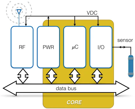
a common data and VDC power buses: 1) RF transceiver, 2) power supply and regulating
electronics, 3) signal processing and control unit, and 4) sensor(s) I/O interface, in addition
to the sensor(s) itself, Fig. 1.1. The complete system is then encapsulated in a bio-compatible
package customized for the specific application, while the volume of a micro-controller based
discrete realization of the system is currently reduced to a several tens of cubic millimetres
with the weight of only a few grams [1]. However, inherently, a general purpose discrete
microcontroller is not optimized for implantable telemetry system applications. Consequently,
their resources are drastically under-utilized and therefore they are not efficient primarily in
terms of size and also power consumption in order of tens or hundreds of mW. Thus, if the
overall implantable system is to be reduced to the size of todays micro-controller chip and
below, and (hopefully) the power consumption reduced to a few hundreds ofµW, naturally the
discrete realization must be replaced by custom ASIC design. In this thesis, we present the
initial advances in design of an application specific core architecture aiming to replace three of
RF PWR 𝜇C I/O
CORE
data bus
sensor VDC
Figure 1.1: A typical block diagram of an implantable RF system consisting of four principal system-level blocks and external sensor.
telemetry system which was designed by using analog signal processing techniques and circuits
at PCB level [2]. The objective of this thesis are:
• To develop a digital controlling and processing core optimized specifically for signal
processing, power management, and sensor(s) I/O functions.
• To develop an FPGA-based prototype for testing and verifying the controlling and
pro-cessing core before proceeding to the actual CMOS IC implementation.
• To create an application-specific integrated circuit (ASIC) layout for the designed
con-trolling and processing core by synthesizing the FPGA-based prototype.
1.3
Organization of the Thesis
In this thesis, an FPGA-based prototype for processing and controlling core of a wireless
im-plantable telemetry system is designed, developed and verified. We also designed and
pre-sented the layout of the ASIC based on the FPGA-based prototype. In Chapter 2, the wireless
telemetry system is explained. More specifically, the processing and controlling core of an
im-plantable telemetry system is described in detail. Finally, concept of FPGA-based prototyping
for ASIC design is discussed. In Chapter3, an FPGA-based processing and controlling core
for an implantable telemetry system is proposed. The experimental results of testing the digital
core is described in Chapter 4. The FPGA-based digital core is integrated to the debugging
interface and its performance is tested within the whole system. In addition, the layout of the
FPGA-based prototype is presented in this chapter. Thesis summery and achievements of this
work are presented in Chapter 5. In addition, some ideas for improvement of the designed
Wireless Implantable Telemetry System
Backgrounds
In this chapter a general overview of the implantable telemetry system and its required
back-grounds are presented. The architecture of telemetry systems is explained with emphasis on
the controlling and processing core. Moreover, FPGA-based prototyping of ASIC design is
discussed.
2.1
Implantable systems
Implantable systems refer to devices inserted into a living body, during medical science
re-search studies and clinical processes for one of the following purposes:
• monitoring physiological parameters such as blood pressure, blood volume, temperature,
etc.,
• treatment of some diseases such as cardiovascular diseases,
• drug delivery,
• and to restore neurological functions for disabled or disorder individuals.
Therefore, using implantable systems can improve life quality and health factors. They
also help scientists and researchers to get valuable information about what is happening inside
of a living body. Usually the implantable systems are called implantable telemetry systems.
The word telemetry is used for communication systems that collect the data from a remote
or inaccessible point and transfer them to a base station for further processing [3]. They are
used in various applications such as healthcare, space and satellite communication, and
envi-ronmental monitoring. Telemetry systems can be implemented wire-line or wireless, however,
implantable telemetry system designed wirelessly for safety and convenience of the patient and
to be controlled remotely. These systems collect the data from corresponding sensors and send
them to the receiver while receiving the controlling commands as well. The sensor interface,
the power regulation module, the digital controlling and processing core, and the RF
front-end which transmits and receives wireless data, are four main modules of every implantable
telemetry system [3]. There are several challenges in designing these systems since they are
going to be implanted inside a living body. The system size and providing power for the
sys-tem are the most important engineering-related challenges. The syssys-tem size must be small
enough to be implantable in a living body. More specifically, for a small laboratory animal
the implanted device should be miniaturized. Power requirement of the implantable system
depends on where it is located inside the body, its function, its lifetime and the required radio
propagation range covered by the system. In high reliability applications such as pacemaker,
defibrillator and infusion pump, a reliable power source is required. However, the available
physical space for the battery is highly limited in these systems and it is a big issue especially
for miniaturized implantable systems. The battery used in these systems should be replaced in
the specific time interval depends on the power consumption of the system. In some
applica-tions such as cochlear implants or retinal visual prostheses [4], the system powered wirelessly
to save the space occupied by the battery, and to reduce complexity and power consumption of
the system. This method usually uses inductive coupling to power the system continuously or
important factor to be considered. In addition, data rate and bit error rate (BER) are the other
aspects of the systems [3].
There are plenty of implantable systems for neurological applications. Deep Brain
Stim-ulator (DBS) is used for neuroglial disorders related to the involuntary movement such as
tremor/Parkinson or mental disorders such as obsessive compulsive disorder(OCD) [6]. In this
method, an implantable device is used to send electrical impulses by a stimulation probe to a
specific region of the brain. It can adjust the electrical signals of the neural cells or chemicals
within the brain. In [6] the most recent DBS system on chip (SoC) is presented. This is the first
closed loop DBS with two-way wireless telemetry and wireless powering. In [7] the first
wire-less switched-capacitor based stimulating (SCS) SoC for Deep Brain Stimulation is presented.
This system uses inductive capacitor charging to increases the power efficiency of the system.
As mentioned before, monitoring physiological parameters is another important application
of implantable telemetry systems. To monitor these parameters, wireless telemetry systems are
used over wireline systems to allow free movement of the patient and to prevent any
incon-venience and infection by the wires. There are different wireless telemetry systems designed
to monitor in vivo parameters. For example, in [8] a multiple channel implantable
teleme-try system for monitoring gastrointestinal (GI) physiological information is presented. In [3]
SmartPill capsule GI Monitoring System is used to monitor human GI tract pressure. This
system includes an ingestible capsule, a receiver, and a display software. To treat glaucoma, a
disease which causes blindness in people, continuous monitoring intraocular pressure (IOP) is
required. Two low power wireless systems for intraocular pressure(IOP) monitoring are
pre-sented in [4] and [5]. In addition, for bladder pressure monitoring a wireless telemetry system
consists of an implantable device, an external RF receiver and a wireless battery charger is
presented in [9].
The cardiac parameters are other important physiological parameters needed to be
moni-tored in plenty of applications such as cardiac parameters monitoring of small laboratory
In addition, monitoring cardiac parameters is helpful to early diagnosis and prevention of heart
problems [11]. In [12] a wireless, fully implantable system is described for cardiovascular
pressure monitoring with a medical stent. In [13] an implantable system for blood pressure
monitoring is presented. For monitoring blood pressure of small laboratory animal, a wireless
implantable system is presented in [14]. The implantable system has 6.4 mm diameter with a
length of 4 mm while dissipating 300 µW power. In [15] a telemetry system for monitoring
blood pressure and blood volume is presented with the weight of 27 g; i.e. not small enough
for implanting in body of small laboratory animals. In [16] a miniature implantable telemetry
system is presented for monitoring blood pressure and blood volume of small laboratory
an-imals. The system occupies 2.475 cm3 volume and weights 4.01 g and consumes power of
150µWin the sleep mode and consumes power of 19.95 mW in the full operational mode. We
explain this telemetry system architecture with detail in Section 2.2.
2.2
Architecture of implantable telemetry system
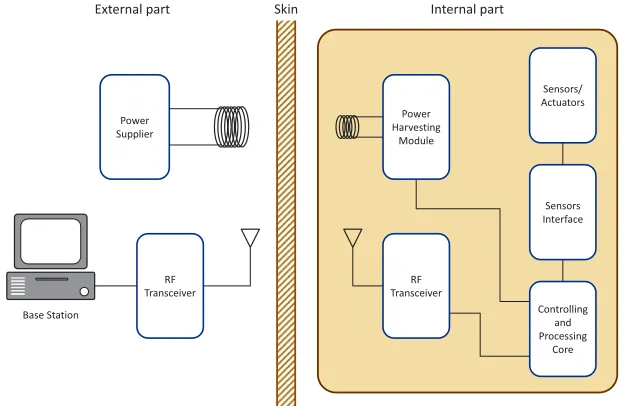
A typical telemetry system composes of an internal part which is implanted into the living
body and an external part which is located outside of the body as shown in Fig. 2.1. The
internal part includes sensors and actuators to collect the data, sensor interface for converting
the collected data to appropriate electrical signals, digital controlling and processing core to
sample and digitize the analog signals, RF front-end to transmit and receive data, and power
module for harvesting system power. The power module and the RF front-end can be designed
generally for different types of implantable telemetry system whereas the other modules should
be specifically designed for a determined application. The external part of the system includes
the power supplier which provides the electrical power of the system usually by using inductive
coupling, the data transceiver for transmitting and receiving the data, and the base station which
is a computer or a specific designed embedded system.
Power Harvesting
Module
Sensors/ Actuators
RF Transceiver
Sensors Interface
Controlling and Processing
Core Power
Supplier
RF Transceiver
Skin
External part Internal part
Base Station
Figure 2.1: Architecture of a typical wireless implantable telemetry system, showing exter-nal and interexter-nal parts of the system. The exterexter-nal part includes power supplier, work station and RF transceiver and the internal part includes power harvesting module, RF transceiver,
sensors/actuators, sensors interface, and controlling and processing core.
telemetry system for cardiac monitoring in small laboratory animals are the size and the power
consumption of the system. The telemetry system proposed in [16] is a miniaturized wireless
system implantable into the body of small laboratory animals e.g. mice to measure blood
pressure and volume data of their heart. The system captures the desired data using appropriate
sensors, digitizes the data, and then transfer it wirelessly to a base station for more processing.
The physical layer of the implanted device includes four main components: Power Module,
Sensors Interface Module, Processing and Controlling Core, and RF front-end.The function
and operation of each module is described with detail in Section 2.2.1
2.2.1
Sensors Interface Module
The sensors interface module provides excitation signal for sensors to generate output signal,
and convert the analog signals of the sensors to appropriate data for controlling and processing
core. Thus, the interface module acts like a bridge between catheters and the other parts of the
2.2.2
Power Module
Power module is responsible to provide power required by all the other modules. There are
two main methods widely used for providing power to implantable medical devices: using
battery [18] which has limited lifetime and should be replaced surgically after several years,
and using an inductive coupled link to recharge the battery [19] wirelessly or to power system
continuously [5]. This method avoids infections and costs caused by replacing the battery [20].
The inductive coupling uses two coils for transferring the power. The transmitting coil is placed
out of the body and is responsible to deliver power to the receiving coil. The receiving coil is
a component of the implanted device and harvests power for the device [21]. In [16], power
module provides power of 3.6 V DC for the whole system. The power module is composed
of a battery, lowdropout regulator, supervisor device, and an analog switch for the interface
module. The system modules have access to the power through the main bus.
2.2.3
RF Front-end
The RF front-end of the telemetry system is responsible for transmitting the data out of the
body and receiving the commands from base station. It is composed of antenna, matching
network, RF transceiver, and clock sources. There are several protocols used at physical layer
of RF transceiver. The power and frequency range of the protocol must be proper for the human
tissue. Therefore, protocols such as Bluetooth, ZigBee, WiFi, and non-standard 2.4 GHz are
appropriate for physical layer of the implantable telemetry systems. In [17] the RF transceiver
works with Frequency-Shift-Keying (FSK) Modulation and frequency of 2.45 GHz.
2.2.4
Controlling and Processing Core
The controlling and processing core is responsible for sampling the analog signals of the
in-terface module, converting it into digital form, preparing it for RF transmitter, managing the
con-trolling power consumption of the system. The two main components of the concon-trolling and
processing core are ADCs and controlling module. The controlling and processing core of the
implantable telemetry system are typically implemented using microcontroller or ASIC. In [22]
a microcontroller-based multichannel implantable telemetry system forin vivo monitoring of
physiological parameters is presented. The output signals of three sensors are connected to
a multiplexer whose output is connected to an ADC. The microcontroller controls the select
lines of the multiplexer to determine which sensor output should be passed to the ADC input.
In addition, microcontroller is responsible for encoding the data and transfer them to the
trans-mitter, verifying the accuracy of data using error-checking algorithm, and controlling power
consumption of the system by switching it from normal mode to low power mode. The size
and power consumption of the system makes it suitable forin vivomonitoring of physiological
parameters in humans not small animals. In [23] a microcontroller-based implantable telemetry
system with smart RF front-end and ZigBee wireless link is presented. The analog front-end
is configured by setting several parameters in microcontroller firmware, which controls
corre-sponding electrical switches. By using this method, it is possible to connect different kind of
sensors to the implantable device and thus use the system for monitoring different
physiolog-ical parameters. Since the system utilizes ZigBee specification for wireless link, the ZigBee
stack protocol is implemented on microcontroller firmware. The dimension of the implant are
48 mm× 33 mm× 15 mm and they claimed it can be further reduced by embedding ZigBee
transceiver and a 8051 µC unit in a 7 mm × 7 mm chip using the CC2430. The
transmis-sion power of the system required for the ZigBee communication is reported as 13.33 µW.
In [1] a microcontroller based discrete prototype version of an implantable telemetry system
is presented which is suitable for monitoring blood pressure and volume data of medium size
animals such as rabbits. The volume of this discrete realization of the system is reduced to a
several tens of cubic millimeters with the weight of only a few grams.
In [8] a low power controlling and processing ASIC is developed for in vivomonitoring
18-bits sigmadelta ADC, a serial peripheral interface (SPI) communication unit, an energy
management, and a low clock control unit. The capsule can work normally for 136 hours with
three 1.5 V 22-mA button batteries. The size of the system is 5 mm in length and 11 mm in
diameter suitable for transmitting the GI physiological information in humans.
2.3
FPGA based Prototyping
The idea of the field programmable array started in 1984 after the first programmable array
logic devices (PALs) are introduced in early 1980s. Actually, the PALs composed of
cus-tom logic block arrays encompassed by I/O blocks, which can be connected or disconnected
by the user. The first FPGA manufactured by the Xilinx Company including 1000 identical
gates using 85000 transistors fabricated in a 2-µm process. The fast growing of
semiconduc-tor technology and the high cost of the ASICs made the FPGA an appropriate replacement
of the ASICs and a proper platform for prototyping various systems and ASICs. The FPGA
technology continued to grow rapidly in 1990s so that in the late 1990s they could support
hardware implementation of most designs. In addition, producers of FPGAs developed the
required tools for simulation, synthesize and implementation of the designs on the FPGA.
In-tellectual Property (IP) was produced to facilitate implementation of communication systems,
signal processing and computational algorithms. The cost of FPGA was reduced significantly
from 1990 to 2003. In addition, the development in nanometer chip processing technology
leads to increasing the number of FPGA slices and therefore the number of gates which can
be made using these slices. It allows the implementation of some advanced circuits on
FP-GAs such as frequency synthesizer (PLLs and DLLs), I/O interfaces, memories, math function
blocks, or signal processing blocks. Another important capability which is added to the new
FPGAs is ability to implement soft processor and embedded systems and thus a whole SoC
on the FPGA. Some tools were developed to make the design and implementation of the
the hardware or software platform design in deep detail. For example, Xilinx EDK and SDK
are two tools for developing a hardware of the embedded system with desired peripherals and
developing the software platform for the embedded system as well. Todays, FPGA are widely
used in communication systems design such as software-defined Radio (SDR) since
implemen-tation of the signal processing blocks becomes very easy using the tools such as Xilinx system
generator which makes the user independent from involving in digital hardware design in deep
level. Furthermore, the IP cores which are the pre-designed common blocks are provided by
the FPGA companies to help users implement their design more quickly. The main advantage
of the FPGAs over ASICs are their ability of reconfiguration. Although in the past the FPGAs
were slower, consumed more power and have lower efficiency than ASICs, the recent FPGAs
such as Xilinx Virtex7 is more efficient in power consumption, speed, and functionality
com-pare with ASICs. FPGA-based prototyping is a method to develop a digital or mixed signal
circuit on programmable devices. It is a suitable technique to test and verify functional
opera-tion of a circuit by connecting the prototype circuit to the other part of the system. Since the
circuit is developed on a programmable device, debugging the error and circuit modification is
easy. In addition, the design is relatively fast, the simulation and verification is simple, and the
cost is low enough. The FPGA-based prototyping solutions are used to determine the accuracy
of both signal processing and controlling algorithms. In [24] a computational algorithm for a
control system is implemented as a hardware design using an FPGA. In [25] an FPGA-based
prototype is used before the ASIC design to test and verify the performance of a proposed
wireless endoscopy system. The prototype verifies the low power consumption of the system.
2.4
Summary
In this chapter, a literature review on implantable telemetry system with various applications
is presented. Furthermore, the architecture of a typical wireless implantable telemetry system
Controlling and Processing Core
3.1
Design Overview
As it is mentioned in Chapter 2, a real time implantable telemetry system captures the analog
data of the physiological parameters, and then transmits it to a computer or a specific
de-signed embedded system for further processing. The processing and controlling core of the
implantable telemetry system has three main functions:
1. It samples the analog signals of the physiological parameters and digitize them.
2. It stores the captured data in memories and read them when the memories are full or
when it receives a send request from the base station. It prepares the data and transfers
them to the RF front-end for transmitting to the external base station.
3. It controls the output command signals, the operation mode, and the power consumption
of the system. Furthermore, it processes the commands which it receives from external
base station.
To accomplish these tasks a CMOS ASIC includes analog-to- digital converters (ADCs),
frequency synthesizers, memories, a controller unit, and I/Os is required, Fig. 3.1. To reduce
the power consumption of the implantable system, in the design of the digital core we apply
I/O
controller memory CORE
time management
CLK
ADC
Figure 3.1: The IC core block diagram with I/O, controller, time management, clock
distribu-tion tree and memory blocks.
several techniques that can be controlled by the user remotely. Globally, the system works
in three modes of operation: continuous mode, duty-cycle mode, and sleep mode. This
strat-egy allows user control of power on/offof the system as necessary, and therefore improve the
power consumption of the system [26]. In addition, the duty cycle mode allows choice of the
desired time interval for capturing and transmitting the data, thus to avoid unnecessary power
consumption. Another technique for reducing the power dissipation, is to decrease the system
clock frequency [27]. However, there are different criteria for clock frequency of each
com-ponent in the controller unit. We can enhance power consumption of the system by choosing
different clock frequencies for each component [28]. Finally, we used clock gating [29] to
disable the high frequency clock in sleep state and therefore reduce the power consumption of
the system. In this chapter, the design and implementation of the mixed signal controlling and
processing core is explained.
3.2
Controlling and Processing Core Firmware
Our custom digital control core consists of the following sub-blocks: I/O, Controller, Time
Management, and Memory. The I/O sub-block is responsible for all interaction with ADCs,
architecture used for the telemetry system and is responsible for signal management and
op-erational mode control. Clock distribution is achieved via the Time Management sub-block.
Lastly, the memory subblock contains all stored on-board sensor data, To provide behavioral
modeling of the controlling and processing core, very high speed integrated circuits hardware
description language (VHDL) is used.
3.2.1
Controller Module
As we mentioned in Section 3.2 this module controls the functions of the system including
acquisition of the collected data, controlling output command signals, processing signals
re-ceived from the external base station and controlling the power consumption of the system.
To reduce the power consumption, the system works in three modes of operation: continuous
mode, duty cycle mode, and sleep mode. This allows us to power off the system when it is
not in use and wake it up when necessary, and therefore improve the power consumption of
the system. The duty cycle mode allows us to choose required time interval for capturing and
transmitting the data and avoid consuming power unnecessarily. The user can choose each of
these modes of operation by sending command to the implantable device. In addition, in this
work, the controller unit works with a low clock frequency for data acquisition and a high clock
frequency for controlling data transmission and processing the commands received from base
station. Finally, the controller employs clock gating to reduce the dynamic power consumption
of the system [29]. Indeed, after the transmitting or receiving task is done in one clock cycle,
the core switches to the sleep state automatically in which only the low frequency clock is
working and the high frequency clock is turned off.
To implement the controller unit, we designed two state machines. One of these state
machines is responsible to control the power consumption of the system while the other one
controls the specific function of the system. We describe each of these state machines with
Controlling the power consumption of the system
As we mentioned in this section, the system works with three modes of operation: Continues
Mode, Data Cycle Mode and Sleep Mode.
1. Continuous Mode: In continuous mode, the system enters the data acquisition state
where sensor data is repeatedly sampled by the ADC and stored in memory. This process
continues until the memory is full and a transmission output control signal is generated
to indicate transmission must occur. While in Continuous mode, the system enters into a
receive state at regular time intervals set by internal receive state counter. For example,
the system may be set to accept external commands every 1min or some other preset
interval.
2. Duty Cycle Mode: In this mode, the system operates similar to continuous mode
how-ever, its operational on/offtime are controlled by two independent counters. For example,
the system may sample data continuously for 1min and enter offstate for 7min, i.e. run
12:5% duty cycle. The system enters sleep state once the duty cycle window is closed.
To reduce system power consumption, ADCs and main system clock are powered down
during duty-cycle offperiod and in sleep state. The choice of duty cycle is the application
specific.
3. Sleep Mode: In this mode, the controller is in sleep state where the main system clock
and ADCs are disabled with only the 200kHz clock active to reduce power consumption.
The system stays in this mode in indefinitely unless awaken via external commands or
internal timers.
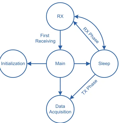
Fig. 3.2 shows the state machine which controls these three modes of operation.
Controlling Function of the Core
The main function of the controller is controlling the data acquisition and output command
Continues Mode
Sleep Mode
Duty Cycle Mode
Figure 3.2: Operation modes of the system implemented as a state machine
RX
Main
Data Acquisition
Sleep Initialization
R X P
has e
TX Ph ase
First Receiving
the module works at five states: Initialization, Data Acquisition, Receiving, Sleep, and Main
State. The tasks of each state are explained as follows.
Initialization state: Upon digital core power-up, clocks, timers and acquisition modes are
initialized in this state.
Data acquisition state: In this state the ADC is enabled by setting the ADC enable signal
to capture and digitize the analog data. Then, system goes to the main state to check if it is
required to transfer data to the transmitter.
Receiving state: Every 10 ms the receiver is enabled to start a new command receiving.
The receiving time interval is 10ms. After receiving is done, the radio is turned off. A counter
is used to keep the receiving time interval.
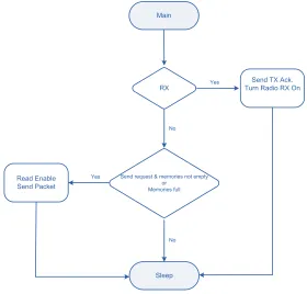
Main state:The main state is responsible for controlling output command signals and to
process signals received from the external base station. As it is shown in Fig. 3.4, first, it is
checked if the system is on transmitting or receiving phase. If transmitting is enabled, it checks
whether the memory is full or the base station requested sending the packets. In these case, the
send-packet signal is enabled which indicates that the packet should be sent to the RF front-end
using the serial peripheral interface (SPI) protocol. If the memory is full the read enable signal
is set to enable reading the data from the memories. In the case that the receiving is enabled the
transmitting acknowledgement is sent to the base station and the radio receiver is turned on.
Once the main tasks are completed, the controller transitions into sleep state where the 1MHz
clock is disabled and only the 200kHz clock is active. The controller remains in sleep state
until awaken by the sleep timer or the next acquisition period.
Clock Gating
Clock gating is a method for enabling or disabling the clock of a sequential circuit. To enable or
disable the clock a signal called ”clock enable” is used in this work. Fig. 3.5 shows the circuit
that generates the clock enable signal. When transmitting or receiving is done the clock enable
Main
Send request & memories not empty or
Memories full
Send TX Ack. Turn Radio RX On
Read Enable Send Packet
RX
Sleep
Yes
No
Yes
No
Figure 3.4: Flowchart of the main state of the controller unit which is responsible for con-trolling output command signals and to process signals received from the external base station .
sleep state. For waking up the system, the clock enable signal is set with the rising edge of the
low frequency clock.
In this work, the clock enable signal is applied to the clock enable input of the BUFGCE
which is a global clock buffer with clock enable. This clock buffer is provided by FPGA for
power saving. The global clock buffer of FPGA is driven by a timing management circuit to
remove timing delay and prevent clock skew. The global clock lines of FPGA are driven by
global clock buffer.
3.2.2
Time Management Module
The Time Management module is responsible for the generation and distribution of clock
sig-nals to different subblocks of the digital core. In this design, the digital core is sourced from an
D Q
Clk
Q
D Q
Clk
Q sleep
200KHz 2MHz
clk_enable sleep_state
Figure 3.5: the designed circuit which creates the clock enable signal for clock gating
ADC
FIFOs Input Clock
FADC
FMemory
FLow
FHigh
Clock Manager
Controller Unit
CORE CORE
Figure 3.6: Time Management Module: clock distribution of the controlling and processing core.
system, Fig. 3.6. This module generates different clock frequencies for the ADC, memories,
and the controller module. The ADC and the memories work with the same clock frequency
based on the sampling rate of the data. The controller module works with two different clock
frequencies, a low clock frequency for the data acquisition and a high frequency clock for main
processing. The clock frequency of the data acquisition is the same as sampling rate of the data
Figure 3.7: Nexys4 DDRTM FPGA evaluation board includes Xilinx Artix-7 FPGA and some peripherals which is used here as a hardware platform for implementing the controlling and processing core.
3.3
Prototyping the Designed Core with FPGA
As we mentioned before developing a CMOS IC for the controlling and processing core, an
FPGA-based prototyping is a high-efficiency low-cost solution for hardware verification. Thus,
in this work we prototyped the designed ASIC on the FPGA to validate its functionality before
fabricating it.
In this work, we developed an FPGA-based prototyping for the controlling and processing
core using the Nexys4 DDRTM Artix-7 FPGA evaluation board to test the designed core on
the Xilinx Artix-7 FPGA. Fig. 3.7 shows the Nexys4 DDRTM FPGA evaluation board which
is the hardware platform for controlling and processing core.
The Nexys4 DDR board includes Xilinx Artix-7 FPGA, various peripherals such as
ex-ternal memories, accelerometer, temperature sensor, microelectromechanical (MEMs), digital
microphone, a speaker amplifier, and some communicational interface such as USB, Ethernet,
PWM audio output and VGA output. Artix-7 FPGA is a 7-series Xilinx FPGA which is proper
more logic per watt in comparison with earlier devices. Furthermore, the Xilinx 7-series FPGA
includes integrated independent dual 12-bit, 2 mega samples per second (MSPS), 17-channel
ADCs.
In this work, For testing the FPGA prototype, a 20 KHz sinusoidal signal is applied to
it as an input signal which is generated by a designed debugging interface. The sampling
rate of the ADC is 200 kilo samples per second (KSPS). Therefore, the ADC data should be
captured every 5 micro seconds to ensure no data are lost. The controller module works with
two clock frequencies: 200 KHz and 2 MHz. The transmitting and receiving are done by the
clock frequency of 2 MHz while data acquisition is done by the clock frequency of 200 KHz.
After the transmitting or receiving task is done in one clock cycle, the core switches to the
sleep state in which only the clock frequency of 200 KHz is working. The state remains in
the sleep till the next rising edge of 200 KHz clock happens. Fig. 3.8 shows the functional
block diagram of the digital core implemented on the FPGA. There are four main units: Xilinx
ADC (XADC), mixed-mode clock manager (MMCM) unit, memory bank (FIFOs), and the
controller unit which are described in Section 3.3.1, Section 3.3.2, Section 3.3.3 respectively.
3.3.1
Analog to Digital Converter Module
To sample and quantize the analog signals of the sensors, an ADC is used in the digital module.
The Artix-7 FPGA has its own on-chip ADC called XADC, which is a dual channel 12-bit
ADC with 17 auxiliary analog input channels and sampling rate of 2 MSPS. It can accept both
bipolar and unipolar analog inputs which are described in Section 3.3.1 and Section 3.3.1. The
ADC has two series of registers: control registers and status registers. The digitized data of
the internal sensors or external analog inputs are stored in status registers and the controlling
data are stored in control registers. Each status register is assigned to one of the analog input
channels or sensors by a specific address. The digitized data are stored in the corresponding
status register. The data structure of the status register is shown in Fig. 3.9. XADC provides
FIFO
FIFO
ADC MMCM Controller
FIFO Demux . . . FIFO1 FIFO2 FIFO3 S3S2S1S0
VAUX N2 VAUX N3 VAUX N10 VAUX P2 VAUX P10 VAUX P3 VAUX N2 VAUX N3 VAUX N10 VAUX P2 VAUX P10 VAUX P3 SW5 SW4 Clk_IN 100MHz Clk Clk_Main Clk_out2 (200 KHz)
Clk_out3 (2 MHz)
Clk_out1 (20 MHz)Switch_mod (1:0) Din (11:0) Clk Din (11:0) Clk Din (11:0) Clk Dout(11:0) Valid Dout(11:0) Valid
Dout(11:0)
Valid Send_Tx_Ak rd_en LED0 Send_Packet Radio_Rx RX_en Tx_en Sleep_en LED1 LED2 LED4 LED3 LED5 Channel_out (3:0) DRDY_out Do_out (15:0) D_in Do_en ADC_en ADC_en Rd_en Rd_en Rd_en Send_rqst Send_rqst Demux . . . S3S2S1S0
Wr_en
Wr_en
Wr_en
Figure 3.8: Functional block diagram of the complete controlling and processing core circuit
15 14 13
. . .
5 4 3 2 1 0Data [11:0] Note
16 bits
Figure 3.9: Data structure of the ADC status register. The converted data of each analog input signals are stored in a specific status register of the ADC.
significant data and the other 4 lowest significant bits (LSBs) can be used to enhance resolution
during data processing such as averaging or filtering, or to decrease the quantization error.
Unipolar Mode of the XADC
In this mode the analog signal on the positive input voltage (Vp) should be always positive and
the negative input voltage (Vn) should be connected to the analog ground or a common mode
signal externally. The differential range of Vp-Vn is 0.0 V to 1.0 V. Vn can change between 0.0
0 0.5 1.0
Maximum voltage on VP
VN (Common mode)
V
ol
ts
1.5
VP , VN
Common mode range
Figure 3.10: Unipolar input signal range of XADC
__ __ __ __ __ __ __ _ _ _ _ _ _ _ _ _ _ _ _ _ _ FFF FFE FFD 004 003 002 001 000 Full Scale Transition Output Code 1 2 -B it O u tp u t C o d e ( H e x)
Input Voltage (mV) Full Scale Input = 1V 1LSB = 1V / 4096 = 244 μV
Figure 3.11: Unipolar transfer function of XADC, showing 12-bit output code vs. voltage of the analog input signal
of the XADC.
In this thesis, the analog inputs are applied to the system in the unipolar mode. The analog
ground and the input voltage are applied to the Vn and Vp inputs of the ADC respectively. The
unipolar transfer function is shown in Fig. 3.11. As it is shown in the figure, the input voltage
in the range of 0.0 V to 1.0 V is transferred to 12-bit digital data. The input signal is applied to
__ __ __ __ __ __ __ __ __ __ _ _ _ _ _ _ _ _ _ _ _ _ _ _ _ _ _ _ _ _ 7FFh 7FEh 002h 001h 000h FFFh FFEh FFDh 801h 800h Output Code
(Two’s Complement Coding)
1 2 -B it O u tp u t C o d e ( H e x)
Input Voltage (mV) Full Scale Input = 1V 1LSB = 1V / 4096 = 244 μV
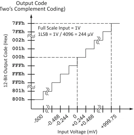
Figure 3.12: Bipolar input signal range of XADC
Bipolar Mode of the XADC
In this mode the analog signal has both positive and negative value with respect to a common
mode voltage. The data stored in the status register as a signed integer which is represented
by the two’s complement. The maximum voltage of the signal Vp should not exceed 1.0 V
and the reference voltage is less than+0.5 V as shown in Fig. 3.12. In this mode also the true
differential signal can be used as an analog input. In this case, the Vp is positive and Vn is
negative input voltages, with respect to a common mode voltage. In this case the differential
input signal cannot exceed 0.5 V and the reference voltage should be in the range of 0.25 V up
to 0.75 V. Fig. 3.13 shows the bipolar transfer function. As it is shown in the figure, the input
voltage in the range of -0.5 V to+0.5 V is converted to 12-bit digital data.
XADC Operating Modes
Since there are several sensors and analog input channels for XADC, different operating modes
are defined to cover the different combination of these inputs. Some of these modes are
__ __ __ __ __ __ __ __ __ __ _ _ _ _ _ _ _ _ _ _ _ _ _ _ _ _ _ _ _ _ 7FFh 7FEh 002h 001h 000h FFFh FFEh FFDh 801h 800h Output Code
(Two’s Complement Coding)
1 2 -B it O u tp u t C o d e ( H e x)
Input Voltage (mV) Full Scale Input = 1V
1LSB = 1V / 4096 = 244 μV
Figure 3.13: Bipolar transfer function of XADC, showing 12-bit output code vs. voltage of the analog input signal
Single Channel Mode:
In this mode just one channel is selected as an analog input of the ADC.
Automatic Channel Sequencer:
When a combination of on-chip sensors and external analog inputs are required to be monitored
by the system, this mode is a proper option. In our work, we use this mode because ADC
captures blood pressure, volume and commnad data from base station and therefore we need
three external analog channels.
XADC Timing
The interface between the XADC and FPGA is called DRP (Dynamic Reconfiguration Port)
and the input clock of the DRP is called DCLK. All of XADC timing is synchronized to this
clock. In addition, ADC generates an internal clock called ADCCLK, which is not
accessi-ble externally. The frequency of this clock is a fraction of DCLK frequency in accordance to
sampling rate of ADC. There are two timing modes for XADC: continuous mode and event
previous conversion finished while in the event mode we need to initiate every sampling and
conversion cycle using a trigger signal called convert start (CONVST). In this work, we
gen-erate this signal in controller unit and applied it to the CONVST input of ADC to control the
power consumption of the system. In this method, ADC only starts conversion cycle at rising
edge of this signal. The timing diagram of event mode is shown in Fig. 3.14. As the figure
shows, the ADC converts the analog signal to digital data in two steps, conversion phase and
acquisition phase. In the acquisition phase, voltage on the selected channel charges a capacitor
of the ADC input in a specific time proportional to the input impedance of the selected
chan-nel. when the rising edge of CONVST take places, analog data is sampled and busy signal
goes high on the rising edge of DCLK. The conversion cycle starts on the next rising edge of
ADCCLK right after the CONVST rising edge event happened. The high value of busy signal
indicates that the conversion cycle is started. When the conversion cycle is finished the busy
signal goes low and after four clock cycles of the ADCCLK, EOC signal goes high for one
DCLK cycle. The low-to-high transition of EOC indicates that converted data are transferred
to the status register successfully and it is ready to use. Four ADCCLK cycles after the current
conversion process is finished the next conversion process will be started.
In this work, the ADCCLK frequency is 6.67 MHz, and the sampling rate is 200 KSPS.
Therefore, there is more than 4 clock cycle between two conversion process. The DCLK
frequency is 20 MHz.
XADC Configuration summary
To set control registers of the XADC and configure it for a specific application, integrated
system environment (ISE) or Vivado design suite provides a wizard. By using this wizard, it is
more convenient to configure the XADC as desired. In this work, the frequency of the analog
signal applied to the input of the ADC for test and debugging is 20 KHz. In accordance to
Nyquist theorem the sampling rate of the ADC should be at least twice the highest frequency
Acquisition Time (N) Min Settling Time (N+1)
1 85 102test
DCLK
ADCCLK
CONVST
BUSY
EOC/EOS
CHANNEL[4:0]
ADC Conversion Time (N)
1 2
Sampling Edge (N)
Channel for N-1 Channel for N
Conversion Finished (N)
20 21 22 23 24 25 26
Figure 3.14: XADC Event-Driven sampling mode. Sampling the analog input starts exactly on the rising edge of CONVST signal while the conversion cycle starts on the next rising edge of ADCCLK
KSPS. To have sampling rate of 40 KSPS for each channel of the ADC, the sampling rate of
the ADC must be 120 KSPS. However, the minimum sampling rate of the XADC is 154 KSPS.
Thus, in this work, we chose sampling rate of 200 KSPS for the XADC.
3.3.2
Memory banks
To store ADCs output data of three channels, we used three FIFO memories in this work. FIFO
memory is a suitable choice for storing and reading data in sequence. To build FIFO memories
we used Xilinx LogiCoreTM IP FIFO Generator. This IP core provides Native interface FIFOs
and AXI4 interface FIFOs. Native interface FIFO cores are suitable solution for buffering,
converting the width of data by choosing different writing and reading widths, and changing
the clock domain by writing and reading data in different clock domains. Native interface
FIFOs uses Xilinx block RAM, distributed RAM or built-in FIFO resources to implement
high performance and low-area FIFOs. AXI4 interface includes three type of AXI4 interfaces:
AXI4-Stream, AXI4 and AXI4-Lite. AXI4 supports all of Native interface applications plus
application AXI System Bus and point-to-point high-speed applications. Native interface is an
appropriate choice for this work.
Clk
wr_en
Rd_en
empty
full
Figure 3.15: Waveform for a typical write and read operation of FIFO
first-word fall-through (FWFT) read operation. In standard mode, when the read enable signal
(Rd en) goes high by the user and there is at least one data to be read (EMPTY is low), the data
appears in the output bus of the FIFO in the next rising edge of CLK and the Valid signal goes
high to indicate that the data outputs are valid. When all stored data of the FIFO are read, the
empty signal is asserted to indicate that the FIFO is empty. If any read operation is requested
when the FIFO is empty, the read request is ignored and the Valid signal stay low. In first-word
fall-through (FWFT) read operation, the first stored data appears in the output bus of the FIFO
automatically without triggering the Rd-en signal. In this mode when the first data is available
on the FIFO output bus, the Valid signal is asserted while the empty signal is deasserted. When
Rd en goes high, the next available data appears on the FIFO output bus. Thus, in the FWFT
read operation, when empty and valid signal goes high and low simultaneously to indicate that
the FIFO is empty while in standard read operation valid signal goes low one clock cycle after
empty signal is asserted. The standard read mode is suitable for this work as we need to have
data on the FIFO output after assentation of Rd en signal.
Fig. 3.15 shows the waveform for a typical write and read operation of the FIFO. In this
work, the same clock used for both write and read operation. When the converted data is ready
on the ADC’s output the write enable signal (Wr en) is set to write the data into the FIFO.
FIFO
Clk
Din [11:0]
Wr_en
Rd_en
Dout [11:0]
Full
Empty
Valid
Figure 3.16: Signal interface of the FIFO used in the controlling and processing core to store the ADC output data
ADC_Dout(11:0)
Data_valid
Channel_out(3:0)
FIFO1_Din(11:0) FIFO2_Din(11:0) FIFO3_Din(11:0)
. . . Demux
Figure 3.17: Demultiplexer interface which is designed to select the right FIFO for writting the data of a specific analog channel
Xilinx FPGAs include 7 series. In our design the writing clock is the same as the reading
clock. Fig. 3.16 shows the signal interface of configured FIFO module. The FIFO works with
the clock of 20 MHz. As it is shown in the Fig. 3.17 a demultiplexer chooses the appropriate
FIFO for writing the data according to the channel output of the ADC. The data are read from
the FIFOs when they are full or when it is requested from the base station.
3.3.3
Clock Management Module
As we mentioned in Section 3.1, we need different clock frequencies for various functions
of the processing and controlling core. The input clock of the FPGA is provided by a 100
MHz crystal oscillator on the evaluation board and the other required clocks are made out of
this input clock by using mixed-mode clock manager (MMCM) primitive in the FPGA. The
range of frequencies, minimize the clock jitter, and deskew clock. The 100 MHz input clock
of the FPGA is applied to the MMCM as the reference clock of the frequency synthesizers. A
20MHz clock is used for the internal ADC and memory units that is further divided down to
200 kHz for data acquisition sampling rate. In addition, a 2MHz clock is generated as the main
processing clock. Since the MMCM provides minimum 5 MHz output clock frequency, we
made the 200 KHz and 1 MHz clocks dividing the 10 MHz clock by 50 and 10 respectively.
The dividing is done using two counters. To configure the frequency synthesizer of MMCM
unit the Xilinx MMCM wizard is used.
3.4
Summary
The controlling and processing core for an implantable telemetry system is developed in this
chapter. The design is FPGA-based prototype of an ASIC design to verify the performance
of the designed digital controlling and processing core. The hardware includes three channel
ADC, frequency synthesizers, memory bank, and a controller module using FSMs. The three
channel ADC is responsible to capture the analog data of the physiological parameters such as
blood pressure and blood volume and convert it to digital signal. The FSMs control the
opera-tion mode of the system which is defined by the operator in the workstaopera-tion and received by the
telemetry system. In addition, FSMs control the data acquisition, receiving and transmitting
modes of the system. Each module in the design works with a specific clock frequency which
Simulation and Experimental Results
In this chapter, the results of behavioral simulation and timing simulations are presented. In
addition, the synthesized layout of the digital core is shown and the results are compared with
the similar works.
4.0.1
Behavioral Simulation Results
Before synthesizing the core, we performed a behavioral simulation on it to confirm the
func-tionality of the core. Indeed, this simulation just verify the RTL code without considering the
timing delays. For simulating the core, it is required to develop a test bench which generates
the appropriate input signals for the core. In this work, we generated the output signals of the
ADC- DRDY (data ready), Channel OUT(channel of the data), and DO (output data of ADC),
the input clock, Input which determine the operation mode of the system, and the send request
command.
First, we simulated the core in continuous mode of operation. Fig. 4.1 shows the data
acquisition and transmitting phase of the system. As it is shown in the figure, this phase starts
every 50µsas it is the sampling rate of ADC. In the beginning of this phase, the ADC en signal
is set to enable the ADC capturing the data. The state changes between data acquisition, main
and sleep states. When the system switches to sleep the high frequency clock, clock of 2 MHz,
0 2 4 6 8 10 0 1 2 Time (µsec) Clk_200KHz
0 2 4 6 8 10
0 1 2
Time (µsec)
Clk_2MHz
0 2 4 6 8 10
0 1 2
Time (µsec)
ADC_En
0 2 4 6 8 10
0 2 4
Time (µsec)
State
Data Acq. Main Sleep Data Acq. Main Sleep
Figure 4.1: Simulated data waveform showing data acquisition and transmitting phase of the system, signals shown: Low frequency clock (200 kHz), High frequency clock (2 MHz), ADC enable, and Controller state.
0 1 2 3 4 5 6 7 8 9 10
0 1 2
Time (µsec)
Clk_200KHz
0 1 2 3 4 5 6 7 8 9 10
0 1 2
Time (µsec)
Clk_2MHz
0 1 2 3 4 5 6 7 8 9 10
0 1 2
Time (µsec)
full
0 1 2 3 4 5 6 7 8 9 10
0 1 2
Time (µsec)
Rd_en
0 1 2 3 4 5 6 7 8 9 10
0 1 2
Time (µsec)
Send_packet