OPTIMIZATION OF 60-GHZ DOWN-CONVERTING
CMOS DUAL-GATE MIXER USING ARTIFICIAL
BEE COLONY ALGORITHM
1HAMID BOUYGHF, 2BACHIR BENHALA, 1ABDELHADI RAIHANI 1
LSSDIA, ENSET Mohammedia, University of Hassan II Casablanca, BP 159 Bd Hassan II, Mohammedia –Morocco.
2
LEAB, Faculty of Sciences, University of Moulay Ismail, BP 11201 Zitoune, Meknes – Morocco.
E-mail: [email protected]
ABSTRACT
In this article, we present an application of the Artificial Bee Colony (ABC) Algorithm for the optimal design of RF analog circuit designed to the telecommunication systems. This work illustrates down-conversion CMOS mixer with high conversion gain and improved Noise Figure (NF). After a presentation of the used algorithm, an application the optimum sizing of a dual-gate mixer (DG-MOSFET) is introduced. The proposed mixer converts input radio frequency signal of 60GHz to frequency output signal of 10GHz. The local oscillator frequency is 50GHz and a local oscillator power considered at 0dBm. The conversion gain of this mixer is -1.87dB and noise is 0.97dB. The results are validated by simulation under ADS and compared with already published works.
Keywords: Optimization, ABC Algorithm, DG-MOSFET, Frequency Mixer, CMOS 45nm.
1. INTRODUCTION
Miniaturization and integration of device and electronic circuits continue to increase which makes the circuit design, more and more, very complicated. Optimal sizing of analog circuitry remains the bottleneck in the flood of analog design, which grows designers to invoking conventional engineering methods and approaches based on statistics [1].
The problem with these methods is that they are often very slow and they do not guarantee convergence to a global optimum. The use of an automatic method of sizing of analog components, to accelerate efficiently the process of analog design circuits is required.
Methods based on the use of heuristics appeared then to resolve optimization problems [2]. Among these heuristics, some are adaptable to many different problems referred to as Meta heuristics. They always offer approximate solutions for optimization problems at a very reasonable times [3]. Some (meta-) heuristics are also proposed in the literature and are used by the
designers, such as Tabu Search [4], Genetic Algorithms (GA) [5], local search (LS) [6], etc. However, the metaheuristics that gave the best results are those of nature inspired, they are inventive, resourceful, efficient, and easy to use and are known as SI: ‘Swarm Intelligence Techniques’ [7]. The SI techniques focus on animal conduct in order to develop some meta-heuristics which can mimic their problem resolution abilities, such as Particle Swarm Optimization (PSO) [8], Ant Colony Optimization (ACO) [9,10,11] and, recently, Artificial Bee Colony (ABC) [12].
In this work, we focus on the use of an Artificial Bee Colony (ABC) to the optimal sizing of CMOS dual-gate frequency mixer for the Radio Frequency (RF) field.
3195 The forth section highlights the results of the optimization, finally, concluding remarks are given in the last section.
2. ARTIFICIAL BEE COLONY ALGORITHM
Artificial Bee Colony (ABC) algorithm was proposed by Karaboga in 2005, for optimizing numerical problems [13, 14]. It is a population based stochastic optimization algorithm inspired by the intelligent collective foraging behavior observed in the bee colony.
The position of a food source represents a possible solution to the optimization problem and the nectar amount of a food source represents the quality (fitness) of the associated solution. The colony of artificial bees contains three groups of bees [15]:
The employed bees The onlooker bees The scout bees
First of all, the set of food source positions is generated randomly asxi
(
i=1,K,SN)
, which is a D-dimensional vector. D corresponds to the number of optimization parameters. The variables contained in each vector must be optimized.After initialization, the population of solutions is subjected to repeated cycles, MCN is C=1, 2…MCN the maximum cycle number. These cycles represent the research process made by the employed bees, the onlooker bees and scout bees. At the end of the research process, the employed bees share information on nectar food sources and their locations with onlooker bees that evaluate these information from all employed bees and choose food sources according to the Pi probability value, associated with this source, calculated by the following expression (1):
∑
= = SN 1 n n i fit i fitp (1)
Where fit is the fitness value of the solution (i) i which is proportional to the amount of the nectar of the food source in the position (i).The employed bees looking in the vicinity of the previous source
i
x
New sourcesv
i that offer more nectar. So as toproduce a candidate food position from the old one in memory, the ABC uses the following expression (2):
(
ij kj)
ij ij
ij x x x
v = +φ − (2)
Where k∈
{
1,2,L,BN}
(BN is numbers of employed bees) andj∈{
1,2,L,SN}
are randomly selected indices. Although k is randomly determined, it must be different from i. φij is arandom number belonging to the interval [-1, 1], it controls the production of a food source in the vicinity ofx . ij
The food source whose nectar is abandoned by the bees, scouts replace it with a new source: If, during a predetermined cycle number called limit, a position cannot be improved, then this food source is assumed to be abandoned. Assume that the abandoned source isx andi
{
1,2, ,D}
j∈ L , then the scout discovers a new food source to be replaced withx . This i operation can be defined as in (3):
( )
(
j)
min j max j min j
i
x
rand
0
,
1
x
x
x
=
+
−
(3)The increase in the number of scouts encourages the exploration process while the increase of onlookers on a food source encourages the exploitation process.
The main procedures of the algorithm are given below:
Initialize REPEAT
Move the employed bees into their food sources and determine their nectar amounts. Place the onlookers into the food sources and determine their nectar amounts.
Move the scouts for searching new food sources.
Memorize the best food source found so far.
UNTIL (the requirements are met).
3195 RF V RF V m_rf .g out R π 2 ) RF (w a (t) RF V ) OL w RF (w a (t) IF V Gain Conv_ = − = out rf _ m
v
g
R
2
G
π
=
used: The number of the food sources which isequal to the number of employed or onlooker bees (SN), the value of limit and the maximum cycle number (MCN) [15].
Detailed pseudo-code of the ABC algorithm is given below [15]:
ALGORITHM 1: Pseudo Code for The ABC Algorithm
3. APPLICATION EXAMPLE
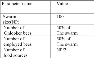
[image:3.612.307.506.117.240.2]The proposed MATLAB implemented algorithm parameters are given in Table 1. The number of iterations of the ABC algorithm is equal to 10000.
Table 1: The ABC Algorithm Parameters
Parameter name Value
Swarm size(NP) 100 Number of Onlooker bees 50% of The swarm Number of employed bees 50% of The swarm Number of food sources NP/2
The ABC algorithm is applied to optimal sizing of the frequency mixer presented by the figure1 (See fig 1 in the appendix (A)).
In this structure, the RF signal is applied to RF gate transistor, and LO signal at LO gate transistor. This topology can realized with two cascode transistors. RF transistor operate in saturation region for giving the high transconductance (gm_rf) that is in function with drain voltage(Vds) of RF transistor and controlled by LO signal which its operated in linear region and work as switch.
One of advantages stated above cascode mixer has another major advantage over single device mixer is that the RF and LO signals can be applied to the separate gate to achieve improved isolation [16].
3.1 Calculations and Equations of Mixer
Output resistor calculation of mixer is determinate using the equivalent model of mixer circuit in small signal presented by the figure2 (See fig 2 in the appendix (A)):
The conversion gain is done by equation (4):
(4)
Then
Initialize the population of solutions
(
i 1 SN, j 1 D)
xi,j = L = L
Evaluate the population Cycle=1
Repeat
Produce new solutionsvi,jfor the
employed bees by using (2) and evaluate them.
Apply the greedy selection process.
Calculate the probability values
j , i
P for the solutions xi,j by
equation (1).
Produce the new solutions vi,j
for the
onlookers from the Solutions xi,jselected depending on Pi,j and evaluate them.
Apply the greedy selection process.
Determine the abandoned solution for the scout, if exists, and replace it with a new randomly produced solution xi,jby equation (3).
Memorize the best solution achieved so far
Cycle=cycle+1
3195
+
+
−
+
+
+
=
1 ol _ m ol _ 0 1 ol _ 0 1 outZ
g
.
r
.
Z
r
Z
.
.
1
.
1
R
0_ol 0_ol m_ol 2 0_ol 2 0_olr
r
g
Z
r
Z
r
0 RF _ V outIf
IF
_
V
R
=
≡gb_ol //C 2 //R gd_ol C 2 Z gs_ol //C gb_rf //C 0_rf //r ] gd_rf C ) gs_rf //C S [(R 1 Z = + =
And we have:
(5)
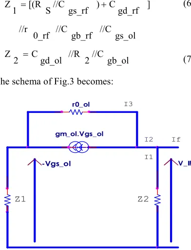
To calculate Rout of our circuit, we must short-circuit the entrance V_RF, then the equivalent model becomes (See fig 3 in the appendix (A)).
To simplify the calculations, we use:
(6)
(7)
[image:4.612.90.286.214.471.2]The schema of Fig.3 becomes:
Fig 4: Equivalent model using equivalent Impedances
Finally, the expression of Rout will be after the calculations:
(8) Therefore, the conversion gain is:
(9)
g m_rf and g m_ol are transconductance of RF and LO transistors respectively and Rs resistor of source. Cgs, Cgd and Cgb refer to parasitic grid to source capacitance, the grid to drain capacitance and
the parasitic grid to bulk capacitance respectively.
3.2 Design Requirement and Specifications for Optimization
For analyzing the dual gate mixer performance, the gain function can be treated as multivariable nonlinear constrained optimization problem and is taken as the objective function for optimization with constraints.
Consider the optimization problems as follows:
Find X= { 1, 2, 3… d }
where
1, 2, … ,
Minimize F X , F X ∈ R
Subject to: G X 0 G X ∈ R ! And
H X 0 H X ∈ R # (10)
(P) inequality constraints to satisfy, (Q) equality constraints to assure, m parameters to manage.
Lower (n) and upper (n) are lower and upper bound vectors of the variable parameters, respectively.
In this section, we deal with the optimal sizing of a CMOS dual-gate Mixer structure regarding the voltage gain presented by the S21 parameter. The input and output matching (via the scattering parameters S11 and S22) and H(x) presents the imposed constraints (saturation of MOS transistors, NF, S11, S22, etc.).
Former to optimize the performances of Mixer, we considerate:
• F(x): The conversion gain function (Objval).
• X: Number of parameters of the problem to be optimized (d=13: 1, 2,…. 13):
W1,2= 1, L1,2= 2, W3,4= 3, L3,4= 4, Lout= 5, Rout= 6, Ce= 7, Lg_rf= 8, Ls= 9, R_mirror= 10, I0= 11, Lg_ol= 12, Cout= 13,
With:
(W1, L1), (W3, L3) are widths and lengths of RF and LO transistors respectively.
- R_mirror: Resistor of current mirror - Cout, Rout, Lout: (LRC) tank parameters.
G(x) represents a set of inequality constraints Ls inductor for source degenerated to be choice in consideration with linearity parameter
(Decreasing our mixer gain see APPENDIX (B)):
3195
deg rf _ m
rf _ m deg
meff
1
g
.
Z
g
)
Z
(
g
+
=
(11)
(See APPENDIX (B))
Minimization expressions of losses for LO signal:
(COL*LOL)-1/$2=0
• H(x) represents equality constraints such as input and output matching (S11 and S22 to be less the -10dB, etc.) of the Mixer.
The conditions of saturation of transistors, are presented by following expressions :
Condition of saturation of MRF transistor :
(Vdd -Vtn) % &sqrt (2*Ids(OL)*LOL/Un*Cox*WOL)+ sqrt (2*Ids(RF)*LRF/WRF*Un*Cox)+I0*Rmirror]
Condition of saturation of MOL transistor :
(I
0* R
mirror- R
out* I
ds(RF)) + V
tn0
The others constraints required for the CMOS Mixer design was the following:
Finput: V_RF = 0.001sin (2*π*fRF*t) fRF = 60GHz
LO : V_LO = 0.69+0.2 sin(2*π*fLO*t) fLO=50GHz with, Power_LO=0dBm
Frequency range: 5~62 GHz
Input impedance Zin: |Zin| = 50 ohm Voltage gain: To maximize
NF with 50 ohm input matching < 3 dB
Therefore, to have optimal performances, the mixer circuit should satisfy the following conditions:
The small size for M_LO transistor could certify a good switching comportment.
The M_LO transistor must be in the linear area.
The M_LO transistor must have a common mode equal to or proximate to its threshold voltage (Vth=0.69V) in order to better exploit the excursion of LO signal and to improve the
switching operation.
The M_RF transistor must operate in the saturation zone to ensure a high g m transconductance and then a good conversion gain as will be demonstrated in the next section.
[image:5.612.308.509.239.315.2]Table 2 presents the specifications of the circuit
Table 2: setting out
Parameter Constraint
[image:5.612.310.508.412.601.2]NF < 3dB
||S11|&|S22| < -10dB
|S21| To maximize
4. RESULTS
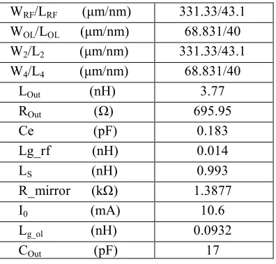
The application of ABC algorithm gives the optimal values of the different variables of the circuit, which are represented in the table3.
Table 3: Optimal Dimensions
WRF/LRF (μm/nm) 331.33/43.1 WOL/LOL (μm/nm) 68.831/40 W2/L2 (μm/nm) 331.33/43.1 W4/L4 (μm/nm) 68.831/40
LOut (nH) 3.77 ROut (Ω) 695.95 Ce (pF) 0.183
Lg_rf (nH) 0.014
LS (nH) 0.993
R_mirror (kΩ) 1.3877
I0 (mA) 10.6 Lg_ol (nH) 0.0932 COut (pF) 17
In order to verify the validity of the results of simulations, which are shown in the following figure, are made in ADS 45nm technology with intermediate frequency F_IF = 10GHz, using the optimal values generated by the application of the ABC algorithm:
4.1 Conversion Loss (S21)
3195
10 20 30 40 50 60 70
0 80
0.5 1.0 1.5 2.0 2.5 3.0
0.0 3.5
freq, GHz
n
f
m2 m2 freq= nf=1.241 nf(2)
10.00GHz
10 20 30 40 50 60 70
0 80
-10 -8 -6
-12 -4
freq, GHz
d
B
(S
(2
,2
))
m4 m4 freq=
[image:6.612.88.265.254.391.2]dB(S(2,2))=-10.056 10.00GHz
Fig 5: The Simulated Return Loss For The Proposed Cascode Mixer
4.2 Noise Figure (NF)
[image:6.612.327.507.455.566.2]The Mixer noise figure simulated at 10 GHz is 1.241dB as shown in Fig 6.
Fig 6: The Simulated Noise Figure For The
Dual-Gate Mixer
4.3 S11-Forward Reflection
As shown in fig.7, we have good isolation and good matching input impedance less than -10dB in the RF frequency. The S11 parameter simulated at 60GHz is -14.399dB.
Fig 7: S11 Parameter versus Frequency
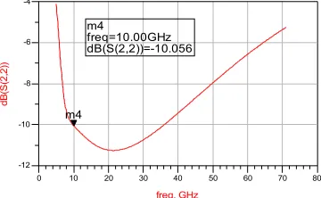
4.4 S22-Reverse Reflection
As shown in fig8, we have good isolation and good matching output impedance less than -10dB in the IF frequency (S22 at 10GHz is -10.056dB).
Fig 8: S22 Parameter versus Frequency
[image:6.612.105.284.508.627.2]3195 the model has shown good matching at the
input (S11
≈
-14dB) and output (S22≈
-10dB).To confirm the validity of the results generated by the ABC method. Figures 5, 6, 7, and 8 show ADS simulations performed using the sizes given in Table 3and they correspond to the results summarized in Table 4. The technology under consideration is 45nm CMOS technology with power supply equal to 1.2 V. We notice that simulation results are in good agreement with those obtained using ABC-matlab technique.
Table 4: Theoretical and Simulation Results
Parameter (dB)
ADS (Simulation)
ABC (Matlab)
S21 -3.178 -1.86623
NF 1.241 0.9687
S11 -14.399 -15.431
S22 -10.560 -10.024
In this case, the conversion gain has assumed to get much higher priority among other design specifications. Table 5 presents a comparison between results obtained using the proposed ABC algorithm and those proposed in the published works [17-18-19]. So, one can easily notice that ABC performances are the competitive (See table 5 in the appendix (A)).
5. CONCLUSION
The presented work proposes an approach for the optimal design of dual-gate Mixer using the Artificial Bee Colony optimization algorithm. The ABC technique was used to optimally sizing of elements forming the Mixer while satisfies the inherent and imposed constraints and maximizes the objective function (conversion gain). Obtained sizing and reached results were first validated through ADS simulations and then compared to those presented in published works. It is shown that the mixer circuit is optimally designed for power gain of -1.87dB and noise figure of 0.97dB. Thus, the design with this optimization approach is useful in finding circuit element values speedily reducing the RF circuit designer time. Now, we are focusing on transforming the proposed ABC mono-objective algorithm into a multiobjective one.
REFERENCES
[1] F. Medeiro, R. R. Macías Fernández, F.V.R. Domínguez Astro, J.L. Huertas, A. R. Vázquez, "Global design of analog cells using statistical optimization techniques", Analog integrated circuits and signal processing, Vol. 6, No. 3, 1994, pp. 179-195.
[2] C.R. Reeves "Modern heuristic techniques for combinatorial problems", Blackwell Scientific Publications, Oxford, 1993.
[3] I.H. Osman, J.P. Kelly (Eds.),"Metaheuristics theory and applications", Kluwers Academic-Publishers, Boston, 1996.
[4] F. Glover, "Tabu search-part II", ORSA Journal on computing, 2(1), 1990, pp. 432.
[5] J. B. Grimbleby, "Automatic analogue circuit synthesis using genetic algorithms",IEE Proceedings-Circuits, Devices and Systems, 147(6), 2000, pp. 319-323.
[6] E. Aarts, K. Lenstra, "Local search in Combinatorial optimization", Princeton: Princeton University Press, 2003.
[7] F. T. S. Chan, M. K. Tiwari, "Swarm Intelligence: focus on ant and particle swarm optimization", I-Tech Education and Publishing, 2007.
[8] M.Fakhfakh, Y. Cooren, A. Sallem, M. Loulou, P. Siarry "Analog Circuit Design Optimization through the Particle Swarm Optimization Technique", Journal of Analog Integrated Circuits & Signal Processing.
[9] B. Benhala, A. Ahaitouf, M. Kotti, M. Fakhfakh, B. Benlahbib, A. Mecheqrane, M. Loulou, F. Abdi and E. Abarkane, Application of the ACO Technique to the
Optimization of Analog Circuit
Performances, Chapter 9, Book: Analog Circuits: Applications, Design and Perfor-mance, Ed., Dr. Tlelo-Cuautle, NOVA Science Publishers, pp. 235–255. 2011. [10] B. Benhala, A. Ahaitouf, A. Mechaqrane, B.
Benlahbib, F. Abdi, E. Abarkan and M. Fakhfakh, Sizing of current conveyors by means of an ant colony optimization technique, The IEEE International Conference on Multimedia Computing and Systems (ICMCS'11), 2011, pp. 899– 904,Ouarzazate, Morocco.
3195 Techniques to the Design of Analog
Circuits: Evaluation and Comparison,” Analog Integrated Circuits and Signal Processing. Springer, vol. 75, No. 3, March 2013, pp. 499-516.
[12] B. Benhala, H. Bouyghf, A. Lachhab, B. Bouchikhi “Optimal Design of Second Generation Current Conveyors by the Artificial Bee Colony Technique”, IEEE International Conference on Intelligent Systems and Computer Vision (ISCV'15), March 25-26, 2015, Fez, Morocco, pp. 1-5.
[13] D. Karaboga, “An idea based on honey
bee swarm for numerical
optimization,”Technical Report-TR06, Erciyes University, Engineering Faculty, Computer Engineering, Department, 2005.
[14] D. Karaboga and B. Basturk, “A powerful and efficient algorithm for numerical function optimization: artificial bee colony (ABC) algorithm,” Springer Science+Business Media B.V. 2007.
[15] D. Karaboga, B. Gorkemli, C. Ozturk and N. Karaboga, “A comprehensive survey: artificial bee colony (ABC) algorithm and applications,” Artificial Intelligence Review, vol. 42, No. 1, 2012, pp 21-57.
[16] M. Nakayama, K. Horiguchi, K. Yamamoto, Y. Yoshii, S. Sungiyama, N. Suematsu,and T. Takagi, A 1.9-GHz single-chip RF front-end GaAs MMIC with low-distortion cascode FET mixer, IEICE Trans Electron E82-C, 717–724, 1999.
[17] Emami, S., Doan, C.H., Niknejad, A.M., and all, “A 60-GHz downconverting CMOS single-gate mixer” IEEE RFIC 2005.
[18] Lai, I.C.H. and all, “60-GHz CMOS Down-Conversion Mixer with Slow-Wave Matching Transmission Lines” IEEE Asian Solid-State Circuits Conference, 2006.
APPENDIX (A)
[image:10.612.84.502.538.684.2]Fig 1: CMOS Dual-Gate Mixer (DG-MOSFET)
Fig 3: Equivalent Model of CMOS Dual-Gate Mixer.
Table 5: 60-GHz Mixer Performance Comparison
Reference
[17]RFIC 2005
[18] ASSCC
2006
[19] EuMC 2009
This work
Process 0.13um CMOS
90nm CMOS
0.13um CMOS
45nm CMOS
Topology Single-gate Dual- gate Dual-gate Dual-gate
RF(GHz) 60 60 60 60
IF(GHz) 2 4 5 10
Conversion Gain(dB)
2 1.2 -2.7 -3.178
[image:11.612.112.508.408.565.2]v
v
1
.
.
1
=
−
Z
degenV
ssZ
cV
RFv
gsv
1V
ddVss
g
mv
gsv
gsG
D
S
Zc
Zdegen
V
RFV
outv
1g
mv
gsout
gs
v
v
=
−
1
.
APPENDIX (B)
Calculation of effective transconductance (gmeff):
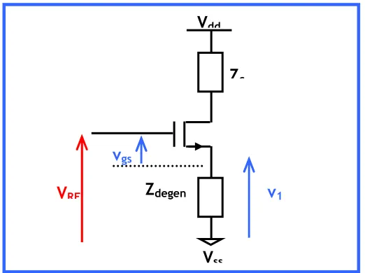
[image:12.612.162.423.171.366.2]Consider the figure 9 below of the transistor charged by a resistor Rc with inductive source degeneration:
Fig 9: MOS transistor with inductive source degeneration
[image:12.612.125.472.417.583.2]Equivalent model of this circuit in small signal is presented by the figure10 below:
Fig.10: Equivalent model of MOS Transistor circuit in small signal with inductive source degeneration
We have:
v
RF=
v
gs+
v
1Then
v
gs=
v
RF−
v
1gs m en RF
gs
v
Z
g
v
v
=
−
deg.
Then
v
RF=
(
1
+
Z
degen.
g
m).
v
gsRF m en
gs
v
g
Z
v
.
)
.
1
(
1
deg