Analysis of the Effect of Temperature and V
dd
on
Leakage Current in Conventional 6T-SRAM Bit-Cell at
90nm and 65nm Technology
ABSTRACT
The increased demand for battery operated portable semiconductor applications and continuous scaling of CMOS devices, results high packaging density but increases the importance of power even more noticeable for a new class of energy constrained systems. Recent Low-Power VLSI design interest is in operating the CMOS circuits with power supply voltage below the transistor threshold operation. As sub-threshold circuits can allow ultra-low power designs to be fabricated on modern CMOS process technology, sub-threshold operation is applicable to wide range of applications ranging from wireless devices, biomedical applications, spacecraft related applications, etc. Lowering the supply voltage to reduce power consumption is one of the choices of the designers for designing low power SRAM circuits. For mobile/multimedia applications of SRAMs, there is a need to reduce standby leakage current while keeping memory cell data. In technology beyond 130nm low-power SRAM is severely complicated by intra die-variations and leakage power. For SRAM cells, leakage reduction has been obtained with low supply voltages and high threshold (HVT) transistors. In this work we have simulated a conventional 6T SRAM cell and analyzed the effect of the leakage and standby currents of 6T cell with respect to various supply voltage (Vdd) and operating temperatures at deep
sub-micron technologies, i.e., 90nm and 65nm CMOS process. Here, the effect of temperature is observed on leakage currents at different supply voltages. As the temperature increases for 400C to 1000C, it is observed that the leakage goes upto 90% in
90nm and 89% in 65nm at Vdd of 1V and 0.5V, respectively.
General Terms
High Threshold Transistors (HVT), Leakage Currents, Deep Sub-Micron Technologies (DSM), Sub-threshold Operations, CMOS Scaling.
Keywords
Threshold Voltage, Temperature Effect, SRAM Bit-cell.
1.
INTRODUCTION
In recent years, portability has become an important issue for mobile multimedia applications. Historically, portable applications were characterized by low throughput requirements such as for a wrist watch, which is no longer true in current
scenario. Among the new portable applications are handheld multimedia terminals, with video display and capture, audio reproduction and capture, voice recognition, handwriting recognition capabilities, and video-on-demands, etc. This computational capacity has to be realized with very low power requirements in order for battery to have a satisfactory life span. Static Random Access Memory (SRAM) has played a key role in high-performance and low-power VLSI applications. Among various embedded memory technologies, SRAM is able to provide the highest performance while maintaining low standby power consumption. SRAM is also fully compatible with logic process technology, which enables a seamless integration of SRAMs with other logic circuits. Meanwhile, the device variation and leakage power are increasing as the miniaturization of the CMOS transistor continues [1,2]. As a result, it has become increasingly challenging in developing SRAM with adequate stability margin for low-voltage operation to address low-power requirements. As the ever-increasing on-die cache memory is taking a large percentage of the total Silicon (Si) area, the power consumption from SRAM has become a crucial factor in the overall power management strategy for advanced VLSI system design. The on-die SRAM power consumption is particularly important for increasingly pervasive mobile and handheld applications where battery life is a key design and technology attribute. Low-voltage operation for SC memories is attractive because of lower leakage power and active energy, but the challenges of SRAM design tend to increase at lower voltage. In this paper we have performed simulation and analysis of a conventional 6T-SRAM Bit-Cell thereafter a comparative analysis is being performed for the leakage currents and standby power at 90nm and 65nm CMOS technology at different operating temperatures to create effect as a practical environment.
This paper is organized as follows, Section II discusses about conventional 6T SRAM. Section III includes components of power dissipation. Section IV has various components which discussed the leakage current analysis and the affect of various parameters and after this in Section V, we have discussed about the standby leakage currents of conventional 6T SRAM at various CMOS technologies.
Neeraj Kr.Shukla
Deptt. of EECE ITM University Gurgaon, India
Shilpi Birla
Deptt. of ECE SPSU Udaipur
Udaipur, India
Kapil Rathi
Design Engineer Texas Instruments
Banglore, India
R.K.Singh
Deptt. of ECE VCT-KEC Dwarahat Almora, India
Manisha Pattanaik
2.
CONVENTIONAL 6T SRAM CELL
The conventional 6T SRAM memory cell is composed of two cross-coupled CMOS inverters with two pass transistors connected to complementary bit-lines. Fig.1 shows this well known architecture of 6T SRAM Cell, where the gate of access transistors are connected to the word-line (wl) to perform the access write and read operations thought the column bit-lines (bl and blbar). Bit-lines act as input/output nodes carrying the data from SRAM cells to a sense amplifier during read operation, or from write circuitry to the memory cells during write operations. The stability and robustness of a SRAM cell is usually evaluated analyzing both its dynamic and static behavior during the typical operations, write, read, and hold. In this paper we analyzed the leakage currents, standby currents at different Vdd and [image:2.612.57.284.247.376.2]temperature. Further there effects are analyzed separately at 90nm and 65nm respectively.
Fig.1 Conventional 6T SRAM Cell
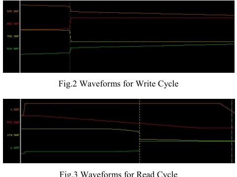
The read and write funaction has been analyse at 65nm. Fig.2 and 3, shows the write and read for 6T SRAM cell at 65nm.
Fig.2 Waveforms for Write Cycle
Fig.3 Waveforms for Read Cycle
As technology is being scaled down, it has its adverse effects apart from the small sizing and several other advantages. Device scaling offers a reduction in gate capacitance at super sub-threshold voltage operation. It offers a reduction in switching energy and gate delay. Device scaling leads to increase in density but at the same time it brought many problems like increased sub-threshold and gate leakage. Due to exponential sensitivities to Vth and Vdd in sub threshold regime, circuit may
not work properly under device scaling. For Battery operated handheld devices, the memory should be small and should operate at low voltage. For designing ultra low voltage
operation, the operating voltage should be below the threshold voltage which is a challenge.
3.
COMPONENTS
OF
POWER
DISSIPATION
There are three different sources of power in CMOS circuits namely, dynamic power (including glitches), static power, and short circuit power. The dynamic component is the power consumed due to charging and discharging of the load capacitance. The short-circuit power, due to crowbar current, dissipated during a switching event when there is a direct path from supply to ground and the glitch power is expected when the inputs to a gate do not arrive at the same time causing a small glitch at the output. Static power is mainly due to sub-threshold leakage power. In the sub-100nm technologies, there is also tunneling through the gate oxide (due to reduced oxide thickness), which produces a thin-oxide gate leakage. As the associated power contribution of this is notable during standby operation, it can be included in the static power. Similarly, the short circuit and the glitch power can be modeled within the dynamic-power equation itself [3] as they occur only when the circuit is switching.
4.
ANALYSIS AND SIMULATION OF 6T
SRAM FOR LEAKAGE CURRENT
The switching current at ultra-low voltage is the sub-threshold leakage current. The sub-threshold leakage current produced by a MOSFET [7] is,
(
)
)
1
(
2 GS t T DSVT
V V
V V T eff
OX eff
leak
V
e
e
L
C
W
I
− −
−
=
µ
η (1)Where, Ileak, µ, Weff, COX, Leff, Vt, VT, VGS, VDS, and η are the
sub-threshold leakage current, carrier mobility, effective transistor width, oxide capacitance per unit area, effective channel length, threshold voltage, thermal voltage, gate-to-source voltage, drain-to-gate-to-source voltage, and sub-threshold swing coefficient, respectively. For devices operating in the weak inversion region, the switching current is exponentially dependent on the voltage levels [4,5]. Alternatively, increasing the device width, produces only a linear increase in the switching current. A linear change in the sub-threshold switching current has a relatively small impact on the voltage transfer characteristics. The sensitivity of the read noise margin to the memory cell ratio is therefore negligible in an ultra-low supply voltage, i.e., sub-threshold memory circuit [6].
4.1 Effect of Temperature on Leakage
Current
The simulation is done to analyze the effect of different temperatures at 00C, 400C, 1000C at 90nm and 65nm on leakage currents.From Fig.4 it is found that the leakage current increases with increase in temperature and voltage. At 1000C
temperature, it rises exponentially with Vdd. In 90nm at T(400C)
and Vdd (0.5V), Ileak is 2.85E-11A while at T(1000C) and Vdd
(0.5V) it goes upto 2.80E-10A, i.e, 90% change. At T(400C) and Vdd (1.0V), Ileak is 4.04E-11A while at T(1000C) and Vdd (1.0V)
[image:2.612.51.291.417.597.2]prominent on the leakage current so as on the power requirements.
Fig.4. Effect of Leakage Current at different Temperatures (00C, 400C, and 1000C) at 90nm
In Fig.5, the simulation results of the effect of leakage currents at different temperatures 00C, 400C, 1000C at 65nm. It is
observed that the leakage current increases with respect to temperature and voltages. At 1000C temperature, it rises
exponentially with Vdd as compared to 00C and 400C, i.e.,
leakage current is more dominating at higher temperature and upto 400C, it is considerable as it can be controlled by other circuit level topologies.
Fig.5. Effect of Leakage Current at different temperatures at 65nm
At T(400C) and Vdd (0.5V), Ileak is 7.91E-12A while at T(1000C)
and Vdd (0.5V) it goes upto 6.32E-11A , i.e., 87% change. At
T(400C) and Vdd (1.0V), Ileak is 8.96E-12A while at T(1000C)
and Vdd (1.0V) it goes upto 1.04E-10A , i.e., 91% change. So,
the device scaling offers the leakage current to rise with temperature. As technology scales the leakage current increases along with the Vdd. So this is one of the major issue , how to
reduce the leakage current at low Vdd with the current scaled
technologies.
4.2 Effect of Technology Scaling Over
Leakage Current
A small increase in the die temperature exponentially increases the sub-threshold leakage current, contrary to the standard higher-voltage circuits designed for high-speed, low-voltage circuits optimized for minimum energy operate faster when the die temperature increases.
The on-chip temperature gradients induced by imbalanced switching activities are therefore typically small across the die of a low-voltage integrated circuit. The die temperature fluctuations due to the variations in the ambient temperature however can cause significant fluctuations in the speed and the power characteristics in ultra low-voltage circuits. Simulation and analysis is performed to see the effect of temperature at various Vdd supply voltages and at different technologies 90nm
and 65nm respectively [7].
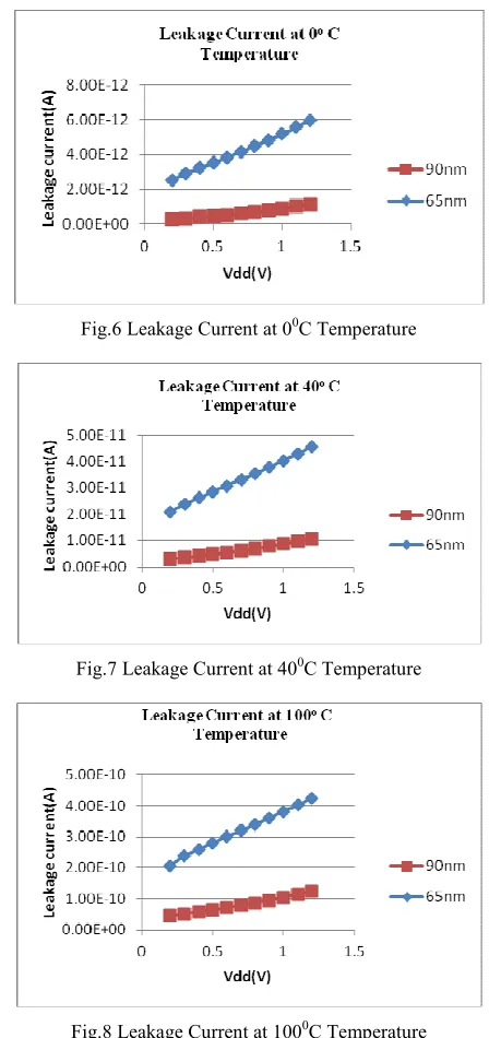
[image:3.612.327.551.229.704.2]As shown in Fig.6, 7, and 8, the effect of leakage currents at different die temperatures 00C, 400C, and 1000C at 90nm and 65nm, we find that the leakage current increases with respect to temperature and voltages. At 1000C temperature, it rises exponentially with Vdd.
Fig.6 Leakage Current at 00C Temperature
Fig.7 Leakage Current at 400C Temperature
[image:3.612.63.280.362.493.2]5. ANALYSIS AND SIMULATION OF
THE EFFECT OF TEMPERATURE
AND V
ddOVER STANDBY CURRENT
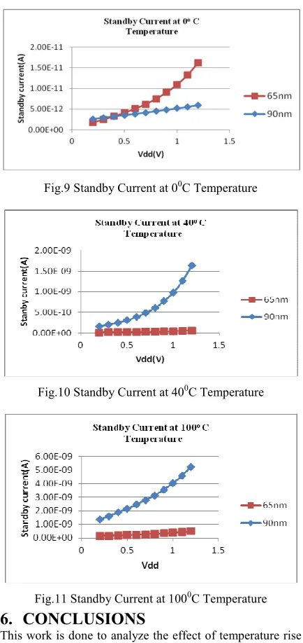
From Fig.9, 10, and 11, we find that the standby current increases at lower technology and this increases power dissipation. Standby current increases more with respect to temperature ,In Fig. 9, 10, when we move from 0oC to 40oC standby current increases as voltage (Vdd) increases and
there is a sharp increase after 0.6V Vdd.
If we compare the leakage current of Fig.6, 7, and 8, we can see that the standby current deceases as the technology becomes lower and it is almost negligible at 65nm while the leakage current increases at lower technology. The graph also shows that the standby current was more at higher temperature and it rises again with the temperature.
[image:4.612.72.289.250.709.2]Fig.9 Standby Current at 00C Temperature
Fig.10 Standby Current at 400C Temperature
Fig.11 Standby Current at 1000C Temperature
6.
CONCLUSIONS
This work is done to analyze the effect of temperature rise and found it very prominent at 90nm technology and as we
scaled down the technology the temperature effect is not so prominent but it increases the leakage current. So we can conclude that the leakage power consumption is mainly due to leakage and stand by current, which increases as we lower down the technologies and this is major challenge as we have to reduce the size and therefore the area (one of the main concern behind the selection of lower technology). As voltage is increasing, the leakage current and standby current is also going up. So, the best option that we have to reduce the power dissipation is to reduce the voltage. But reducing the voltage is not as easy as we have to reduce the sub-threshold voltage which will again increase the sub-threshold currents and moreover in case of SRAM if we reduce the operating voltage, the SRAM stability will be disturbed and so the SRAM will not be able to read and write properly. As we cannot go below the data retention voltage, therefore while reducing the voltage, we have to adopt alternative method which will not disturb the SRAM functionality (stability). For increasing the stability we have come to alternative SRAM cells like 7T, 8T or 10T SRAM Bit-Cells.
7.
ACKNOWLEDGMENTS
The authors are very grateful for their respective organizations for their support and encouragement.
8.
REFERENCES
[1] Jinhui Chen Clark, L.T. Tai-Hua Chen, “An Ultra-Low-Power Memory with a Subthreshold Power Supply Voltage”, Solid-State Circuits, IEEE Journal, vol.41, Oct 2006, Issue: 10, pp- 2344-2353.
[2] Hamzaoglu, F.; Zhang, K.; Yih Wang; Ahn, H.J.; Bhattacharya, U.; Zhanping Chen; Yong-Gee Ng; Pavlov, A.; Smits, K.; Bohr, M , “A 3.8 GHz 3 Mb SRAM Design With Dynamic Stability Enhancement and Leakage Reduction in 45 nm High-k Metal Gate CMOS Technology” , Solid-State Circuits, IEEE Journal ,vol. 44 , no. 1, 2009, pp.148 – 154.
[3] Koichi Takeda et al, “A Read Static Noise Margin Free SRAM cell for Low Vdd and High Speed Applications”, Solid-State Circuits, IEEE Journal,vol. 41, Jan.2006, Issue 1 , pp.113-121.
[4] Peter Geens, Wim Dehaene, “A dual port dual width 90nm SRAM with guaranteed data retention at minimal standby supply voltage”, 34th European Solid-State Circuits Conference, 2008. ESSCIRC 2008.pp-290-293.
[5] Naveen verma, Anantha P. Chandrakasan,”A reconfigurable 65nm SRAM achieving voltage scalability from 0.25 v-1.2V & performance scalability from 20Khz-200Mhz, 34th European Solid-State Circuits Conference, 2008. ESSCIRC 2008, pp-282-285.
[7] Shilpi Birla, Neeraj Kr. Shukla, Manisha Pattanaik, R.K.Singh, “Device and Circuit Design Challenges for Low Leakage SRAM for Ultra Low Power Applications”, Canadian Journal on Electrical & Electronics Engineering Vol. 1, No. 7, December 2010.
AUTHORS PROFILE
Neeraj Kr. Shukla (IEEE, IACSIT, IAENG, IETE, IE,
CSI, ISTE), Ph.D. Scholar at the UK Technical University, Dehradun (Uttarakhand) India. He’s an Asst. Professor in the Department of Electrical, Electronics & Communication Engineering, ITM University, Gurgaon, (Haryana) India. He has received his M.Tech. (Electronics Engineering) and B.Tech. (Electronics & Telecommunication Engineering) Degrees from the J.K. Institute of Applied Physics & Technology, University of Allahabad, Allahabad (Uttar Pradesh) India in the year of 1998 and 2000, respectively. His main research interests are in Low-Power Digital VLSI Design and its Multimedia Applications, Open Source EDA, and RTL Design.
Shilpi Birla (IACSIT, IAENG), a Ph.D. Scholar at the UK
Technical University, Dehradun (Uttarakhand) India and an Asst. Professor in the Department of Electronics & Communication Engineering, Sir Padampat Singhania University, Udaipur (Rajasthan) India. She has received her M.Tech. (VLSI Design) and B.E. (Electronics & Communication Engineering) Degrees from the University of Rajasthan, Jaipur (Rajasthan) India and MITS University, Laxmangarh, (Rajasthan) India, respectively. Her main research interests are in Low-Power VLSI Design and its Multimedia Applications, RF-SiP, and Low-Power CMOS Circuit Design.
Kapil Rathi, Design Engineer at Texas Instruments, India.
He received M-Tech degree in Microelectronics & VLSI Design and B.Eng. degree in Electrical & Electronics Engineering from R.G.P.V. University, Bhopal, India in 2009 and 2005, respectively. His research interests include the low power and high speed SRAM embedded memories.
R.K. Singh (IAENG, ACEEE, IE, ISTE), Professor in the
Department of Electronics & Communication Engineering, VCT-Kumaon Engineering College, Dwarahat, Almora (UK) India. He is being honored with the Ph.D. in
Electronics Engineering in the Year 2003 from the University of Allahabad, Allahabad (Uttar Pradesh), India. He has received his M.E. (Electronics & Control Engineering) in 1992 from BITS, Pilani, Rajasthan) India. He has around thirty five research publications in the conferences and journals at national and international. He has also guided eight ME thesis. He has authored seven text-books in the field of VLSI Design, Basic Electronics, and Opto-Electronics. He has worked at various capacities in the Academic domain such as, the Principal, Kumaon Engineering College, Dwarahat in the year 2003-04, Director (O), Directorate of Technical Education, Uttaranchal in the year 2005, and Joint Director, State Project Facilitation Unit, Dehradun for the World Bank TEQIP Project. Apart from his industrial experience, he contributed as a Scientist and Senior Scientist in Engineering Research at Central Electronics Engineering Research Institute (CEERI), Dehradun (UK) India, with a focus in Fibre Optics Communication and their subsequent application in optical devices to various other technologies and VLSI Design and Con Controls (P) Ltd. He is also the recipient of couple of prestigious awards, e.g., Rastriya Samman Puruskar, Jewel of India Award, Rastriya Ekta Award, Life Time Achievement Award, and Arch of Excellence Award. His current areas of interest are VLSI Design, Opto-Electronics and its applications.
Manisha Pattanaik (IEEE, IE, ISTE) Manisha Pattanaik