RSA Cryptography using Designed Processor and
MicroBlaze Soft Processor in FPGAs
Md. Nazrul Islam Mondal
Dept. of CSE, Rajshahi University of Engineering and
Technology, Rajshahi-6204, Bangladesh
Md. Al Mamun
Dept. of CSE, Rajshahi University of Engineering and
Technology, Rajshahi-6204, Bangladesh
Boshir Ahmed
Dept. of CSE, Rajshahi University of Engineering and
Technology, Rajshahi-6204, Bangladesh
ABSTRACT
Some applications such as RSA encryption/decryption need integer arithmetic operations with many bits. However, such operations cannot be performed directly by conventional CPUs, because their instruction supports integers with fixed bits, say, 64 bits. Since the CPUs need to repeat arithmetic operations to numbers with fixed bits, they have considerably overhead to execute applications involving integer arithmetic with many bits. On the other hand, This paper implements hardware algorithms for such applications in the FPGAs for further acceleration. However, the implementation of hardware algorithm is usually very complicated and debugging of hardware is too hard. The main contribution of this paper is to present an intermediate approach of software and hardware using FPGAs. More specifically, this paper presents a processor based on FDFM (Few DSP slices and Few Memory blocks) approach that supports arithmetic operations with flexibly many bits, and implement it in the FPGA. To show the potentiality of designed processor, 128-bit RSA encryption/decryption is implemented and compare with soft processor “MicroBlaze” in FPGA. The resulting processor uses only one DSP48E1 slice and four Block RAMs (BRAMs), and RSA encryption software on it runs in 0.42ms. However, MicroBlaze uses three DSP48E1 slices and 170 Block RAMs (BRAMs) and runs in 152.28ms. Hence, the proposed designed processor is significantly efficient in terms of resource used and time complexity in comparison to soft processor “MicroBlaze” in FPGAs. Also the proposed processor can be used efficiently for longer bit arithmetic operation such as 2048-bit without further modifications and hence it is more flexible.
General Terms
RSA Security Algorithm
Keywords
Multiple-Length-Arithmetic, MicroBlaze, Soft Processor, Montgomery Modular Multiplication in RSA, FPGA, DSP Slices, Block RAMs.
1.
INTRODUCTION
An FPGA is a programmable logic device designed to be configured by the customer or designer by HDL (Hardware Description Language) after manufacturing. An FPGA chip maintains relative lower price and programmable features [1], [2], [3], hence, it is widely used recently. The readers may refer to see some circuit implementations in FPGAs [4], [5], [6], [7], [8], [9], [10], [11], [12] to accelerate computation.
Applications require arithmetic operations on integer numbers which exceed the range of processing by a CPU directly is called Multiple Double Length Numbers or Multiple Precision
Numbers and hence, computation of these numbers is called Multiple-Length-Arithmetic. More specifically, application requires integer arithmetic operations for multiple-length numbers with size longer than 64 bits cannot be performed directly by conventional 64-bit CPUs, because their instruction sup-ports integers with fixed 64 bits. To execute such application, CPUs need to repeat arithmetic operations for those numbers with fixed 64 bits which increase the execution overhead. Alternatively, hardware algorithms for such applications can be implemented in FPGAs to speed up computations. However, the implementation of hardware algorithm is usually very complicated and debugging of hardware is too hard.
Since, low level of instructions, represented by 0’s and 1’s is an almost impossible to understand even by an expert, the debugging of an algorithm at this level is very hard. Moreover, to implement hardware algorithm, written by hardware language such as Verilog HDL, users should have sufficient knowledge of hardware such as registers which makes it complicated to the non-expert or to the beginners. The instructions in assembly language are written by alphanumeric symbols instead of 0’s and 1’s in low level that is an almost similar to the high level language, written by English which makes the instructions as well as algorithms easy to read, modify and debugging by the non-expert or by the beginners.
The main contribution of this paper is precisely described as follows:
To prove the potentiality of the proposed processor, 128-bit RSA is implemented and compare with soft processor “MicroBlaze” in FPGA which implies that proposed processor is significantly efficient in terms of resource used and time complexity.
Also, the proposed flexible-length arithmetic processor based on FDFM approach can be used for computing of integer numbers with flexibly many bits, even longer than 2048-bit by a single machine instruction.
To make the debugging and further development easy, an intermediate approach of software and hardware is presented.
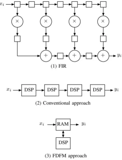
Since, the designed processor based on FDFM approach, the key idea of the FDFM approach is to use few DSP slices and few block RAMs to perform routine computations which can be treated alternatively as a resource efficient approach. Let us explain briefly the FDFM approach using a simple example. Figure 1 (1) illustrates a hardware algorithm to compute the output of FIR (Finite Impulse Response) yi = a0 xi +a1 xi1 +a2
xi 2 +a3 xi 3. A conventional approach implementing the FIR is
[image:2.595.62.269.246.518.2]to use four DSP slices as illustrated in Figure 1 (2)[13]. In this conventional approach, the number of DPS blocks must be the same as that of multipliers in the hardware algorithm. However, FDFM approach uses one or few DSP slices and one or few block RAMs to implement the FIR. The Figure 1 (3) shows the FDFM approach using one DSP slice and one block RAM to implement the same mentioned above. Note that, the coefficients a0,a1 ,. . . are stored in the block RAM.
Figure 1: FDFM approach over conventional one for FIR
[image:2.595.59.284.585.729.2]The readers may refer to the papers [14], [15], [16], [17] in which they can find details about FDFM approach and conventional approach.
Figure 2: Internal Configuration of Virtex-6FPGA
The most common FPGA architecture consists of an array of logic blocks, I/O pads, Block RAMs and routing channels. Furthermore, embedded DSP blocks which is integrated into an FPGA that makes a higher performance and a broader application. Figure 2 illustrates the Virtex-6 FPGA developed by Xilinx. The CLB (Configurable Logic Blocks) in Virtex-6 consists of 2 sub-logic blocks called slice. Using LUTs (Look Up Tables) and Flip-Flops in the slices, various combinatorial circuits and sequential circuits can be implemented.
The summarization of the several significant points of the results is described as follows:
1. A flexible-length-arithmetic processor is proposed for the applications which require arithmetic operations for numbers longer than 64 bits. Even, numbers longer than 2048 bits or higher can be computed by the designed processor without any modification.
2. The proposed processor is flexible in a sense that it can support arithmetic operations for numbers with flexibly many bits or numbers with variable size longer than 64 bits.
3. Finally, the potentiality of this processor is checked by implementing 128-bit RSA and compare with soft processor “MicroBlaze” which shows that the proposed processor is significantly efficient.
The rest of this paper is organized as follows: Section II briefly describes the Multiple-length-arithmetic operation. In Section III describes the proposed architecture. The RSA cryptography as an application is described briefly in Section IV; however the readers may refer to the previous paper [23] for details. Section V describes experimental results and discussions. Finally Section VI concludes this work.
2.
MULTIPLE-LENGTH-ARITHMETIC
OPERATION
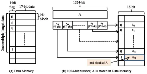
The main purpose of this section is to describe Multiple-Length-Arithmetic operations. Suppose that A and B are two multiple-length numbers of 1024 bits each. These numbers are partitioned into several blocks of 17 bits. First, let us see that how a multiple-length number of 1024 bits is stored in data memory. Figure 3(a) shows a data memory (BRAM). Every 17-bit block data together with 1-bit flag represents a block of 18 bits and MSB (Most Significant Bit) of each bit-block is known as flag which set to 1 indicates the end of each stored multiple-length data into the data memory as shown in Figure 3(b). In this figure, multiple-length data A of 1024 bits is divided into 61 numbers of 17 bits block such as a0, a1, . . .,,
a60, a61. Every 17 bits block of multiple-length data, A
Figure 3: Data of 1024-bit Length is Stored in Memory (BRAM)
For the benefit of readers, Figure 4 describes the instruction memory as well as instruction format of multiple-length or multi-double long data. Figure 4 (a) represents an instruction memory in which 53 bits instruction together with 1-bit flag can be stored at any address of the instruction memory addresses. In this case, 1-bit flag is set to 1 indicates the last instruction for execution. Note that, addresses of the instruction memory are handled by the Program Counter (PC).
Let us give an example of a multiplication of two multiple-length or two multi-double long data. However, other arithmetic operations can also be performed such as addition, subtraction, division, comparison of multi-double long data. Suppose u and v represents two multi-double long data. Let us multiply u by v and the result is stored in w, that is w = u . v. An assembly instruction for this computing of multi-double long data is as follows:
MUL A, B, C
[image:3.595.327.563.78.237.2]In the above instruction, A, B and C are known as operands of 16-bit each which can be used to indicate 216 different addresses 0, 1, . . ., 216 of the data memory (BRAM) and MUL is known as OPCODE of 5-bit which determines the operation of operands (in this case multiplication) as illustrated in Figure 4(b). The readers may refer to the paper [23] for details in which an example is clearly described for multi-double long multiplication. Let us see Algorithm 1 for multiplication of two multi-double long data u and v.
Fig.4.An Instruction Memory and an Instruction Format for Multi-Double Data
Figure 5: The Proposed Processor Architecture Algorithm 1: Multi-Double Long Multiplication
B: number of digits in radix-217 operands
n: last number of digit of radix-217 numbers in u
m: last number of digit of radix-217 numbers in v
Input: u = 𝑛−1
𝑢
𝑖. 𝐵
𝑖𝑖=0 ,v =
𝑣
𝑖. 𝐵
𝑖 𝑚 −1 𝑖=0Output: w=u.v
1. for j=0 to m-1 do
2. c0
3. w0 0
4. for i=0 to n-1 do
5. {c,wi+j} wi+j ui . vj+c
6. End for
7. Wn+jc
8. End for
9. Return 𝑛+𝑚−1𝑖=0
𝑤
𝑖. 𝐵
𝑖Since there is a page limitation, hence the readers may refer to the previous paper [23] to show a simple example of the above algorithm.
3.
PROPOSED ARCHITECTURE
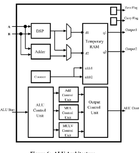
[image:3.595.57.297.530.638.2]Figure 6: ALU Architecture
In the following section, RSA cryptography is implemented using the proposed architecture and it is programmed by assembly language. The assembly instructions of number, 117, each of 54-bit are needed to implement modular exponentiation algorithm. In this paper, only the assembly code is shown for Montgomery Multiplication as illustrated in the previous paper [23]. In below assembly code, the registers R1 and R2 are used to take inputs X and Y , each of 64-bit. Also 64-bit M is given. The registers R3, R4, R5 is used to hold the intermediate results and final results of the Montgomery Multiplication is stored either in R6 or C. Note that, 64-bit data in register R1 is divided into several blocks of 17-bit each and these are stored in several block registers such as R10, R11, R12, R13 (lower block to higher block). For the
case of other registers, these can be explained in similar way.
[Assembly Code for Montgomery Multiplication]
R1=X, R2=Y;
R3=0, R4=0, R5=0, R6=0;
C=0;
R10 , R20, R30; X (R1) Y(R2) store in R3
01: MUL,
02: MOVI, R30 , R40, R33; copy blocks of R3 into R4
03:MASK, R43 , R43, 1FFF; make last 4-bit of R43 as 0’s
04: MUL, R40 , M01R,50; R4M 1 store in R5
05: MOVI, R50 , R40, R53; copy blocks of R5 into R4
06:MASK, R43 , R43, 1FFF; make last 4-bit of R43 as 0’s
07: MUL, R40 , M0, R50; R4 M store in R4
08: ADD, R30 , R50, R60; store R3 + R5 in R6
09: SHR, R63 , R60, 13; 64-bit shift right of R6
0A: CMP, R60 , M0; R6 compare with M
0B: JC, 0D; if R6 > M, go to OD
0C: SUB, R60 , M0, R60; R6-M is the results in R6
0D:MOV, R60 , C0; results in R6 move to C
4.
AN APPLICATION OF RSA
CRYPTOGRAPHY USING THE
PROPOSED PROCESSOR
This section briefly reviews the RSA Cryptography which is described details in paper [15]. Using the proposed processor, the same algorithm is implemented by software, instead of HDL as illustrated in paper [15] to make it easy for modifications or changes by a non-expert or by a beginner.
In RSA [18], the modular exponentiation C = PE mod M or P = CD mod M are computed, where P and C are plain and cypher text, and (E, M) and (D, M) are encryption and decryption keys. Usually, the bit length in P , E, D, and M is 512 or larger. Also, the modulo exponentiation is repeatedly computed for fixed E, D, and M , and various P and C. Since modulo operation is very costly in terms of the computing time and hardware resources, Montgomery modular multiplication [19], [20], [21] is used, which does not directly compute modulo operation.
Montgomery multiplication [19], [20], [21] is an optimal method to calculate modular exponentiation. Three R-bit numbers X, Y , and M are given, and (X · Y + q · M ) · 2−R mod M is computed, where an integer q is selected such that the least significant R bits of X · Y + q · M are zero. The value of q can be computed as follows. Let (−M−1) denote the minimum non-negative number such that (−M−1) · M ≡ −1( or 2R− 1) (mod 2R). Since M is odd, then (−M−1) < 2R always holds. The q can be selected such that q = ((X · Y ) · (−M−1))[r − 1, 0]. For such q, (X · Y +q · M )[r −1, 0] are
zero. The readers may refer to paper [23] for an example.
Radix-2r Montgomery multiplication is shown in Algorithm 2. In Algorithm 2, d = [R/r] presents the number of digits in radix-2r operands. The multiplier Y is partitioned by each r-bit and Yi represents the i-th digit of Y. Therefore, Y could be
given by 𝑌 = 𝑑−1𝑖=0 2𝑖𝑟. 𝑌𝑖. After d loops, R-bit Montgomery
multiplication can be computed. As far as now, Montgomery multiplication could be computed by multiplication, addition and shift operations without modulo operations.
Algorithm 2: radix-2r Montgomery Multiplication
radix-2r, d = [R/r], X, Y, M ∈ {0, 1, ..., 2R− 1},
1
02 .
d
i i
ir
Y
Y , Yi∈ {0, 1, ..., 2 r− 1}
(−M−1) · M ≡ −1 mod 2r, −M−1∈
{0, 1, ..., 2r− 1}
Input: X, Y, M, −M−1
Output: Sd = X · Y · 2−dr mod M
1. S0 ← 0
2. for i = 0 to d − 1 do
3. qi ← ((Si + X · Yi ) · (−M−1)) mod 2r
4. Si+1 ← (X · Yi + qi· M + Si ) / 2r
5. end for
6. if (M ≤ Sd) then Sd ← Sd – M
mod M using the Montgomery modular multiplication, then compute the square (P ·2R mod M ) . (P · 2R mod M ) · 2−R
mod M = P2·2R mod M. It should be clear that, by repeating the square computation using the Montgomery modular multiplication, having PE· 2R mod M. After that, multiply 1, that is (PE· 2R mod M ) · 1 · 2−R mod M =PE mod M is computed. In this way, cypher text C could be obtained.
Algorithm 3 shows the modular exponentiation using Montgomery multiplication of Algorithm 2. In Algorithm 3, Eb represents the size of E. Inputs 22dr mod M and −M−1 are
given. To use Montgomery modular multiplication, C and P are converted from 1 and P in the 1st line and the 2nd line, respectively. The line 1, 2, 4, 5 and 7 in Algorithm 3 can be computed using Montgomery multiplication of Algorithm 2.
Algorithm 3: Modular Exponentiation
0 ≤ E ≤ 2Eb− 1,
1
0 2.
b E
i i
iE
E , Ei∈ {0, 1}
Input: P, E, M, −M−1
, 22dr mod M
Output: C = PE mod M
1. C ←(22dr
mod M ) · 1 · 2−dr mod M ;
2. P ← (22dr
mod M ) · P · 2−dr mod M ;
3. for i = Eb − 1 downto 0 do
4. C ← C · C · 2−dr
mod M ;
5. if Ei = 1 then C ← C · P · 2−dr mod M ;
6. end for
7. C ← C · 1 · 2−dr mod M ;
Let {A : B} denote a concatenation of A and B. For example, if A = (F F )16 and B = (EC)16, {A : B} = (F F EC )16.
Algorithm 4 is an improved algorithm from Algorithm 2. Considering the features of the target Virtex 6 FPGA, radix-217 is selected. Let R denotes the size of Montgomery multiplier operands X, Y, and M. Also, d = [R/17] is the number of digits of the operands on radix-217. In the algorithm, the 17d ≥ R + 3 condition is introduced to ignore the subtraction shown in the 6th line of Algorithm 2. If the condition is satisfied, it can be guaranteed that at least 3-bit 0 is padded to the most significant bits of the most significant digit as the redundancy. Due to the stringent page limitation, the proof is omitted. However, M ≥ C is always satisfied in the modular exponentiation shown in Algorithm 3. Further, in practical RSA encryption, the size of operands is radix-2 numbers such as 512-bit, 1024-bit, 2048-bit, and 4096-bit. For radix-217 system, the condition 17d ≥ R +3 is satisfied. If the condition is not satisfied, then it needs to append one redundant digit at the most significant digit.
Algorithm 4: Montgomery Algorithm
radix-217 , d = [R/17], 17d ≥ R + 3,
X, Y, M, Si∈ {0, 1, ..., 2 R− 1},
−M−1, α, β, γ, C
α, Cβ∈ {0, 1, ..., 217 − 1}, Cγ , CS∈ {0, 1},
1 0 17 . 2 d i i i XX , Xi∈ {0, 1, ..., 217− 1}, Xd= 0
1 0 17 . 2 d i i i YY , Yi∈ {0, 1, ..., 217− 1}
1 0 17. 2 d i i iMM , Mi∈ {0, 1, ..., 217− 1}, Md= 0
1
0 (, )
17 .
2
d
j i j
j
i S
S , S(i,j)∈ {0, 1, ..., 217 − 1}, Sd= 0
Input: X, Y, M, −M−1
Output: Sd = X · Y · 2−17d mod M
1. S0 ← 0
2. for i = 0 to d − 1 do
3. q ← ((X0 · Yi + S(i,0)) · (−M−1)) mod 217
4. Cα, Cβ , Cγ , CS ← 0
5. for j = 0 to d do
6. {Cα: α} ← Xj · Yi + Cα
7. {Cβ: β} ← q · Mj + Cβ
8. {Cγ: γ} ← α + β + Cγ
9. {CS: S(i+1,j −1)} ← γ + S(i,j) + CS
10. end for
11. end for
Algorithm 4 is a radix-217digit serial Montgomery algorithm from Algorithm 2. In other words, each 17-bit, as 1 digit, is processed every clock cycle. For this reason, the operands X, Y , M , and Si are split into 17-bit digits Xj , Yj , Mj, and S(i,j) ,
respectively. The loop from the 2nd to 11th lines of Algorithm 4 corresponds to the 2nd to 5th lines of Algorithm 2. Comparing the two algorithms, Si+1 ← (X · Yi + qi· M + Si )/
2r of the 4th line of Algorithm 2 corresponds to the digit serial processing by 4th to 10th lines of Algorithm 4 . In Algorithm 4, Cα , Cβ , Cγ , and CS are carries and they are added at the
next loop. In the algorithm, Cα, Cβ are 17-bit carries for 17-bit
MACC, and Cγ , CS are 1-bit carries for 17-bit addition. For
example, at the 6th line Xj , Yi are timed and added to 17-bit
carry Cα , the result is 34-bit. A product of Xj and Yi , and an
addition of the product and Cα are computed. The resulting
upper 17-bit denotes a carry Cα which can be added at next
loop. The lower 17-bit of result is α which is used at the 8th and 9th lines. These carries in the algorithm appear in both the 17-bit MACC and the 17-bit adder to prevent a long carry chain that causes circuit delay.
The proposed flexible-length-arithmetic processor architecture is used to implement modular exponentiation algorithm and evaluate on Xilinx Vertex-6 XC6VLX240T-3FF1156, programmed by software and synthesis with Xilinx ISE Foundation 13.4. Table II and Table I show the synthesized result for this work.
For the benefit of readers, an optimal implementation[15] is recalled, which is evaluated on Xilinx Virtex-6 FPGA XC6VLX240T-1, programmed by hardware description language Verilog HDL and synthesized by Xilinx ISE Foundation 11.4. Note that, the optimal one, programmed by HDL is specialized design by an expert so that it is difficult to debug or change by a non-expert or sometimes even by an expert. However, proposed approach is in between software and hardware which makes debugging easy to the non-experts or beginners.
On the other hand, the implementation of RSA encryption/decryption using proposed processor architecture is designed to be implemented by software, more specifically by assembly language; hence it is easy for modifications or changes by a non-expert or by a beginner which makes it flexible. Even though, it has ability to support higher bit (more than 2048-bit) of RSA encryption/decryption.
5.
EXPERIMENTAL RESULTS AND
DISCUSSIONS
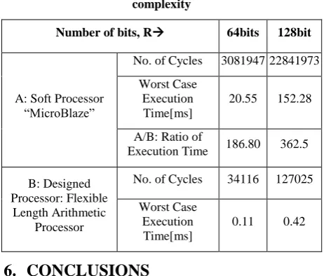
The proposed flexible-length-arithmetic processor architecture is used to implement modular exponentiation algorithm and evaluate on Xilinx Vertex-6 XC6VLX240T-3FF1156, programmed by software and synthesis with Xilinx ISE Foundation 13.4. Table I shows the synthesized result for the work in comparison to soft processor in FPGAs.
Table I and Table II show the synthesized results of Virtex-6 for comparing both implementations. In Table I, it is compared how much resource used to implement RSA Cryptography. In this table, the implementation uses 4 block RAMs and 1 DSP slice. On the other hand, 70 block RAMs and 3 DSP slices are require for the same implementation using soft processor, MicroBlaze in FPGAs. Hence, it is said that this work is more resource efficient.
In Table II, time complexity to implement RSA Cryptography is compared. In this table, the implementation requires 0.42ms. On the other hand, soft processor, MicroBlaze needs 152.28ms for the same implementation. Hence, it is said that this work is more efficient in term of time complexity.
Based on results in Table I and Table II, it is said that, this implementation of RSA encryption/decryption using proposed processor is significantly efficient (less resource used, less time) in comparison to soft processor, MicroBlaze. Also designed processor architecture can be used to implement 256-bit, 512-bit, 1024-bit, even more than 2048-bit RSA encryption/decryption without further modifications or changes. Hence it is flexible.
Table I:Comparison of Resource Used to Implement 128-bit RSA Cryptography
Target FPGA: Vertex-6 FPGA
Designed Processor: Flexible Length
Arithmetic Processor
Soft Processor in FPGA: MicroBlaze
Slice Used 170/301440 6984/301440
Block RAM Used 4/416 70/416
DSP (DSP48E1)
Used 1/768 3/768
Clock Frequency in
[image:6.595.313.546.85.282.2]MHz 299.90 150
Table II: shows the synthesized result to compare time complexity
6.
CONCLUSIONS
In this paper, an intermediate approach of software and hardware is presented using DSP Slices and Block RAMs in FPGAs. More specifically, a flexible-length-arithmetic processor based on FDFM approach is presented that supports arithmetic operations for numbers with flexibly many bits, even longer than 2048 bits. The potentiality of this processor is shown through the implementation of modular exponentiation algorithm and compares it with the implementation results using 32-bit soft processor, MicroBlaze in FPGA. The results in Table I and Table II show that this work is significantly efficient in terms of resource used and time complexity. In future, it can be applied for higher bit RSA cryptography.
7.
REFERENCES
[1] VIRTEX-6 FPGA Memory Resources (V1.5), Xilinx Inc., 2010.
[2] VIRTEX 6 ML605 Hardware USER GUIDE (V1.2.1), Xilinx Inc., 2010.
[3] VIRTEX-6 FPGA DSP48E1 SLICE USER GUIDE (V1.3), Xilinx Inc., 2011.
[4] J. Bordim, Y. Ito, and K. Nakano, “Accelerating the CKY parsing using FPGAs,” IEICE Transactions on Information and Systems, vol. E86-D, no. 5, pp. 803– 810, 2003.
[5] J. L. Bordim, Y. Ito, and K. Nakano, “Instance-specific solutions to accelerate the CKY parsing for large context-free grammars,” International Journal on Foundations of Computer Science, vol. 15, no. 2, pp. 403–416, 2004.
[6] Y. Ito and K. Nakano, “A hardware-software cooperative approach for the exhaustive verification of the Collatz conjecture,” in Proc. of International Symposium on Parallel and Distributed Processing with Applications, 2009, pp. 63–70.
[7] K. Nakano and Y. Yamagishi, “Hardware n choose k counters with applications to the partial exhaustive search,” IEICE Transactions on Information and Systems, vol. E88-D, no. 7, 2005.
[8] Y. Ito and K. Nakano, “Efficient exhaustive verification of the Collatz conjecture using DSP blocks of Xilinx
Number of bits, R 64bits 128bit
A: Soft Processor “MicroBlaze”
No. of Cycles 3081947 22841973
Worst Case Execution Time[ms]
20.55 152.28
A/B: Ratio of
Execution Time 186.80 362.5
B: Designed Processor: Flexible
Length Arithmetic Processor
No. of Cycles 34116 127025
Worst Case Execution Time[ms]
Computing, vol. 1, no. 1, pp. 19–62, 2011.
[9] K. Nakano and E. Takamichi, “An image retrieval system using FPGAs,” IEICE Transactions on Information and Systems, vol. E86-D, no. 5, pp. 811– 818, May 2003.
[10]Y. Ago, Y. Ito, and K. Nakano, “An FPGA implementation for neural networks with the FDFM processor core approach,” International Journal of Parallel, Emergent and Distributed Systems, vol. 28, no. 4, pp. 308–320, 2013.
[11]Y. Ito and K. Nakano, “Low-latency connected component labeling using an FPGA,” International Journal of Foundations of Computer Science, vol. 21, no. 03, pp. 405–425, 2010.
[12]X. Zhou, N. Tomagou, Y. Ito, and K. Nakano, “Efficient Hough transform on the FPGA using DSP slices and block RAMs,” in Proc. of International Parallel and Distributed Processing Symposium Work-shops, May 2013, pp. 771–778.
[13]VIRTEX-6 FPGA DSP48E1 SLICE USER GUIDE (V1.2), Xilinx Inc., 2009.
[14]Y. Ago, A. Inoue, K. Nakano, and Y. Ito, “The parallel FDFM processor core approach for neural networks,” in Proc. of International Conference on Networking and Computing, December 2011, pp. 113–119.
[15]S. Bo, K. Kawakami, K. Nakano, and Y. Ito, “An RSA encryption hardware algorithm using a single DSP Block and single Block RAM on the FPGA,” International Journal of Networking and Computing, vol. 1, no. 2, pp. 277–289, July 2011.
[16]Y. Ito, K. Nakano, and S. Bo, “The parallel FDFM
processor core approach for CRT-based RSA decryption,” International Journal of Networking and Computing, vol. 2, pp. 56–78, 2012.
[17]K. Nakano, K. Kawakami, and K. Shigemoto, “RSA encryption and decryption using the redundant number system on the FPGA,” in In Proc. IEEE International Symposium on Parallel and Distributed Processing, May 2009, pp. 1–8.
[18]R. L. Rivest, A. Shamir, and L. Adleman, “A method for obtaining digital signatures and public-key cryptosystems,” Commun. ACM, vol. 21, no. 2, pp. 120-126, 1978
[19]T. Blum and C. Paar, “Montgomery modular exponentiation on recon-figurable hardware,” in Proc. of the 14th IEEE Symposium on Computer Arithmetic, 1999, pp. 70–77.
[20]P. L. Montgomery, “Modular multiplication without trial division,” Math. of Comput., vol. 44, pp. 519–521, 1985.
[21]A. F. Tenca and C. K. Koc¸, “A scalable architecture for Montgomery multiplication,” in Proc. of the First International Workshop on Crypto-graphic Hardware and Embedded Systems, 1999, pp. 94–108.
[22]M. Niimura and Y. Fuwa, “Improvement of radix-2k signed-digit number for high speed circuit,” Formalized Mathematics, vol. 11, no. 2, 133–137, January 2003 [23] Md. Nazrul Islam Mondal, Kohan Sai, K. Nakano, and