Dynamic Partial based Single Event Upset (SEU)
Injection Platform on FPGA
Reza Omidi Gosheblagh
Ph.D. Candidate
Karim Mohammadi
Professor
School of Electrical Engineering, Iran University of Science and Technology (IUST), Narmak, Tehran 16846-13114, IRAN
ABSTRACT
SRAM based FPGAs are attracting considerable interest especially in aerospace applications due to their high re-configurability, low cost and availability. However, these devices are strongly susceptible to space radiation effects which are able to cause unwanted single event upsets (SEUs) in the configuration memory. In order to mitigate the SEU effects, various methods have been investigated in literatures. Fault injection methods are required to evaluate the efficiency of the hardening techniques. This paper has proposed a dynamic partial reconfiguration based fault-injection platform (DPR-FIP) for emulating the SEU faults in FPGA configuration memory. Besides the SEU faults, DPRFIP tool supports cumulative SEU, multi-event upset, and single event transient faults in combinational parts and flip-flops.
General Terms
Reliability, Digital Circuits, Fault Tolerant Design, Testing.
Keywords
Single Event Effects (SEU), FPGA, Fault injection, Emulation, Radiation Effects, DPRFIP Tool.
1.
INTRODUCTION
SRAM-based FPGA devices are steadily becoming the most suitable platform for implementing modern systems especially in aerospace applications due to their high re-configurability, low cost and availability [1-4]. SRAM-based FPGAs, however, are much more susceptible to single event upsets (SEUs) than ASICs. Single event upsets (SEUs) are caused by space ionizing radiation strikes that discharge the charge in storage elements, such as configuration memory cells, user memory, and registers.
Many SEU mitigation techniques have been proposed in the past years in order to avoid bit flips in the storage cells of microprocessors and FPGAs. A variety of mitigation techniques have been developed to achieve an SEU immune circuit [2, 4-7]. Mostly, redundancy is at the heart of these fault tolerance methods. Redundancy based techniques involve extra components (hardware redundancy), extra execution time (time redundancy), or a combination of both. Each technique has some advantages and drawbacks and there is always a compromise between area overhead, performance, power, and dependability.
Fault injection is important to evaluating the dependability of digital systems. Generally, the fault injection means the deliberate insertion of faults in an operating system to determine its response offers an effective solution to this problem [8].
Fault injection has been widely accepted to carry out SEU sensitivity analysis of FPGA based systems [9]. This can be performed in several ways. Among them, a typical one is the injection of faults by exposing the circuit to radiation. The radiation tests, as physical fault injection techniques, are very fast and can be used when a prototype of the system is available. The main drawbacks of these techniques are the high cost of required facilities and their poor controllability and observability.
The simulation approaches evaluate the SEU effect in hardware description language (HDL) level without any hardware platform [10-12]. Simulation-based fault injection techniques are flexible and have good controllability and observability [3]. However, these techniques require a lot of time to simulate the model of the design and cannot be used for exhaustive fault injection campaigns.
To cope with the time limitations imposed by simulation approach, the emulation techniques have been proposed to take advantage of hardware prototyping, using an FPGA-based hardware emulator [13]. FPGA-FPGA-based fault injection combines the speed of physical-based techniques and the flexibility of simulation-based techniques.
This paper has presented a dynamic partial based fault injection platform (DPR-FIP) for evaluating the SEU effects in SRAM-FPGA. The DPR-FIP tool provides a system that the user deliberately or randomly injects the single or multi upset in the configuration memory of SRAM FPGA. Besides the fault injection in the switch matrixes and the configuration logic blocks, the proposed system is able to inject SEU fault in flip-flops. All data communications for fault injections are based on partial re-configurability of the modern FPGAs, and are performed through the internal configuration access port (ICAP).
This platform is able to inject the fault only in a constrained area of the FPGA. This capability improves the fault injection performance, especially for designs that engage only a portion of the FPGA. Furthermore, the fault injection campaign could be adjusted so that only special resources have been affected. This capability allows the designers to test their hardening techniques with more details. Currently, the DPR-FIP system is able to separately inject fault in switch matrix, configuration logic blocks (CLBs), and flip-flops. This paper aims to completely illustrate the hardware architecture and software details of the DPR-FIP fault injection platform.
we developed in this paper to emulate single event upset on SRAM-FPGAs. The experimental results are presented based on the proposed platform on benchmark circuits in section IV. Finally, section V concludes the paper.
2.
BACKGROUND
The SEU emulation platforms provide a test and verification method for evaluating the impact of soft errors on a given FPGA-based design [14]. To demonstrate the basic concepts of the SEU emulation, it is necessary to review the FPGA structure with more details. In this section, we describe the generic SRAM-based FPGA architectural model to illustrate the SEU effects on design. Moreover, the emulation approaches have been covered in this section.
2.1
SRAM FPGAs Basic Concepts
[image:2.595.58.297.347.544.2]The internal structures of the main FPGAs families are very similar. For Xilinx devices, a grid of configurable logic blocks (CLBs) has been integrated with programmable switch matrixes that connect the logic blocks according to the design requirements (Fig. 1). A CLB element contains some of slices. Every slice contains some logic-function generators (or look-up tables), storage elements, wide-function multiplexers, and so on. These elements are used by all slices to provide logic, arithmetic, and ROM functions [15].
Fig. 1: Virtex-4 FPGA architecture [15]
The configuration of all these internal elements of FPGAs is controlled by a number of bits which are called the configuration bits or bitstream. In SRAM based FPGAs these bits are stored in RAM cells. Some of these bits fill the LUT with the truth table that represents the desired combinational circuit, other bits set the functionality of the storage element as a FF or a latch, and some others set the control inputs of the multiplexers. Another bits turn on/off the switch matrixes pass transistors, allowing for the routing of all the lines of the circuit [16].
The Virtex FPGAs configuration memory is arranged in frames that are tiled about the device. These frames are the smallest addressable segments of the Virtex configuration memory space, and therefore all operations must act upon whole configuration frames. Each configuration frame in the FPGA has a unique 32-bit address that can be divided into five parts: Block type, Top/Bottom indicator, Row address, Major address (column address), and Minor address (frame address in a column). To develop an appropriate fault injection platform, it is required to have a complete
understanding of the configuration memory and frame address. For more details the reader can refer the Xilinx documents [15, 17, 18].
2.2
Fault Models in SRAM FPGAs
As mentioned before, all designs on SRAM-FPGAs are defined by configuration memory. Therefore, to inject faults in FPGA based design, ones should subvert the configuration bits.
In some version of FPGAs, like Xilinx-Spartan series, the configuration memory is integrated. So, the manipulation of the configuration memory requires that all bits have been communicated to the fault injection controller. This process is time-consuming, and increases the fault injection campaign run-time.
By introducing the partial reconfiguration capability on FPGAs, the SEU emulation approaches have been developed. The basic concept of these emulation techniques is based on minimizing data traffic between the host FPGA and the fault injection controller. The configuration memory of these FPGAs, like Virtex series, is divided into frames. So, to create an upset in configuration memory, the fault injection controller should handle only a small portion of host FPGA. This achievement decreases the data traffic between the host and controller, and improves the fault injection run-time.
3.
The DPR-FIP TOOL FOR SEE
EMULATION
The dynamic partial reconfiguration based fault injection platform (DPRFIP) is a system that has mainly developed to inject bit-upset faults within the internal memory of FPGA’s. This system mainly uses the partial reconfiguration capability of modern FPGAs. As mentioned before, this capability significantly decreases the data communications in fault injection campaign, and therefore improves the fault injection run time compared to initial versions of SEU emulators.
DPRFIP system consists of a hardware platform and a software layer. In this section, the hardware and software architecture of the DPRFIP system have been completely illustrated.
3.1
Hardware Architecture
The hardware setup as shown in Fig. 2 consists of three parts. The first part is a personal computer that provides a complete graphic user interface (GUI) to manage and monitor the fault injection process. The second part is a single event effect (SEE) fault controller based on LPC2368 microcontroller. It receives the fault injection modes from PC and controls the configuration memory of the FPGA. All required signalling and timing are managed through the external microcontroller. The third part is the FPGA platform which hosts the Design under Test (DUT) and other modules.
The experimental platform that has been considered is the Zefant-nanov4 board from simple-solutions corporation [19]. It contains XC4VFX12 device, which is a 12,312 logic cell mounted in a 363 BGA (Ball Grade Array) flip-chip package, belongs to the Xilinx Corporation. The Virtex FPGAs offer the possibility to read-back and partially reconfigure the configuration memory at any time.
generator, which includes a linear feedback shift register (LFSR). A comparator is also included to compare the outputs of the DUT and golden instances. Moreover, to handle the configuration memory, some modes are available that include JTAG, Serial slave, SelectMap, and the internal configuration access port (ICAP). The ICAP port is the best one that offers a data bus width up to 32 bits with the maximum nominal frequency of 100Mhz [20, 21], and therefore the DPRFIP tool has used the ICAP port.
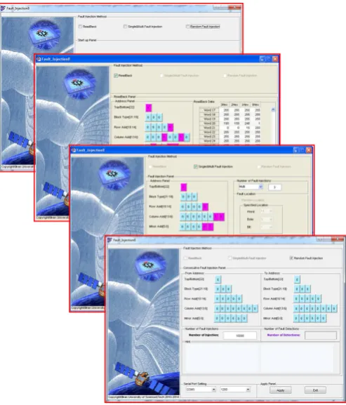
Fig. 4 shows a snapshot of the GUI interface for such application. By means of this interface, it is possible to set up the experiment options, and in particular: i) read-back any deliberate frame, ii) the test mode (the frame address and frame bits can be randomly addressed or these values can be selects by user. Moreover, the faults may accumulate until a functional failure occurs, or the bits may be addressed sequentially, one at a time), iii) the fault type (either a single bit flip or multiple bit flip), iv) FPGA resource type selection for fault injection (switch matrix, logic block, and flip-flops), and v) the address range of memory bits that are involved in the current experiment.
Finally, the external controller is included for purposes of error injection and correction. In following subsections, the details of controller have been illustrated.
[image:3.595.317.564.72.361.2]Fig. 3: Block diagram of hardware setup
Fig. 4: Graphic user interface on PC
3.2
Fault Injection in Combinatorial Parts
To realize a system on FPGA as depicted in left side of the Fig. 5, a high-level description language (HDL), which is used to describe the design and operation of electronic circuits on FPGAs, is synthesized and a netlist is generated. After placement and routing of this netlist, a bitstream is obtained that can be downloaded onto the FPGA. Finally, a set of experiments is performed and the analysis of the circuit responses is made [13].
As previously mentioned, the partial re-configurability allows the users to access a small portion of bitstream on FPGA. When the partial reconfiguration is performed, approximately all functions on FPGA remain active during the reconfiguration. To implement the SEU emulation based on dynamic partial re-configurability, a portion of the original bitstream should be read back from the FPGA configuration memory, and then the modified bitstream should be downloaded into the FPGA configuration memory.
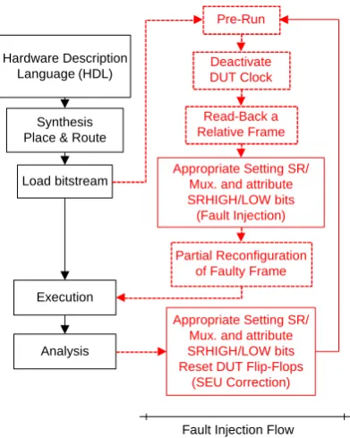
Fig. 5 has depicted the flow diagram for fault injection. This flow, which is performed by the external controller, includes four main phases:
Initialization
SEU injection
Execution and analysis of DUT and Golden units
SEU correction
The initialization phase includes the data communication between the GUI interface and controller, and determines the fault injection mode, area, and so on. Next, in SEU injection phase, a random frame from specified area is read back to the controller. According to the fault injection mode, the frame is modified. Then the faulty frame through the partial reconfiguration capability is rewritten to its original address. This condition means that the FPGA is deposited in a faulty Golden
Unit
Design under Test
(DUT) ICAP
Interface
Host FPGAFault Injection Area Data & Control
Trigger & Enable CMP Error
User Interface
(PC)
µController
Rand Gen.
FPGA Prototype
[image:3.595.54.272.354.461.2]Controller PC
[image:3.595.58.285.503.647.2]state, and the DUT and Golden units are launched to perform their functions.
Following the execution phase, the analysis step monitors the comparator output. When a conflict on outputs of DUT and golden units is observed, the controller increases the relevant variables. Finally, the original frame is replaced instead of the faulty frame. At the same time, all flip-flops are reset; this work corrects the potential propagated fault.
[image:4.595.334.520.105.224.2]In Virtex-4 devices, to configure the configurable logic blocks (CLBs), it is required to load 22 frames on FPGA. According to our experimental results, 19 frames are allocated for switch matrixes and three frames configure the slices. Based on this fact, the fault injection process is distinguished for switch matrixes and logics on DPRFIP tool.
Fig. 5: Fault injection flows in combinational parts
A. SEU Fault Injection in CLB Flip-flops
The storage elements in a slice, which are used in sequential circuits, can be configured as either edge-triggered D-type flip-flops or level-sensitive latches [15]. The current value of flip-flops depends on the implemented design, and directly does not available in configuration bits. Therefore, the dynamic partial reconfiguration methods directly are unable to trigger an upset in flip-flops [13].
According to [13], the only way to change the FFs state in a Virtex FPGA is to apply a set or reset to it. The aforementioned reference implies that it is only possible to pulse the global set/reset (GSR) line of the device that sets or resets simultaneously all the FFs in the device. The actual effect of the GSR line is determined for each flip-flop by the position of a switch. The proposed method in [13] is based on pulsing the GSR line, and therefore the fault injection process on FFs is much more complex than the process previously presented in combinational parts.
In DPR-FIP tool, we use two novel approaches to provide the fault on FFs. The first method is performed through the modification on some switch related to flip-flops (Fig. 6). To create a faulty state in FFs, the SR switch and SRHIGH/SRLOW attribute are used in DPRFIP tool.
The SR signal forces the storage element into the state specified by the attribute SRHIGH or SRLOW. As, the SRHIGH forces a logic High at the storage element output when SR is asserted, while SRLOW forces a logic Low at the
[image:4.595.58.253.235.431.2]storage element output. Fig. 7 represents the procedure of this method.
Fig. 6: Injecting a pulse into a combinational path to create SEU in FFs
As drawback, like the pulsing the GSR line, this method concurrently may affect all FFs in one Slice. Due to the fact that all FFs of the slice use one shared multiplexer on their SR inputs. For Virtex-4 FPGAs, which contain two flip-flops in each slice, if we assume that the logic “1” probability in FFs is one half, the probability of the single fault is equal to 50%. Besides, the probability that both of the FFs have been affected is 25%.
Based on the experimental tests, for virtex-4 devices, we have observed that if both the Set and Reset signals have been added to all flip-flops in design, the Xilinx-ISE tool often synthesizes the flip-flops in the distinguished slices. This guarantees that the proposed approach just affects one flip-flop in each fault injection trial.
Fig. 7: Fault injection flow on FFs based on a pulse into a combinational path
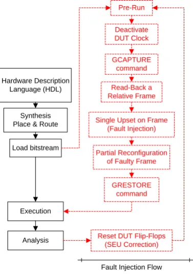
The G-capture/G-restore method is another approach which is supported by the DPRFIP tool to inject a single event upset (SEU) in flip-flops. This approach is based on the global capture and global restore commands of Virtex FPGAs. GCAPTURE loads the current value of the FFs into its INIT configuration bit; and GRESTORE updates the FFs content with the value of the INIT configuration bit. These bits could
Hardware Description Language (HDL)
Synthesis Place & Route
Load bitstream
Execution
Single Upset on Frame (Fault Injection)
Partial Reconfiguration of Faulty Frame
Analysis
Read-Back a Frame
Partial Reconfiguration (SEU Correction)
Fault Injection Flow
Hardware Description Language (HDL)
Synthesis Place & Route
Load bitstream
Execution
Appropriate Setting SR/ Mux. and attribute SRHIGH/LOW bits (Fault Injection)
Partial Reconfiguration of Faulty Frame
Analysis
Read-Back a Relative Frame
Appropriate Setting SR/ Mux. and attribute SRHIGH/LOW bits Reset DUT Flip-Flops
(SEU Correction) Pre-Run
Deactivate DUT Clock
Fault Injection Flow
FF
LATCH
INIT1
INIT0
SRHIGH
SRLOW Q
D CE CK
[image:4.595.324.520.412.657.2]be read back into fault injection controller for the SEU injection purpose. The details of this approach have been illustrated in Fig. 8.
Fig. 8: Fault injection flow on FFs based on G-capture/G-restore method
4.
TEST RESULTS
In order to perform the fault injection of SEUs, the FPGA is configured with the layout described in the previous section. The under test designs have been selected from standard benchmark circuits [22]. The number of injected faults was so selected to guarantee that the gathered results are statistically meaningful. The fault injection campaign is a random process, and therefore more trials provide accurate dependability evaluation results. The sample space, which represents the available states for injecting and classifying of one SEU fault, is related to the engaged bits of the DUT area on FPGA. It is required to mention that the engaged bits in design could be determined through the Xilinx FPGA Editor tool and FPGA related documents [17]. Table I represents the fault injection result on benchmark circuits for one million tests.
Table 1: Fault Injection Results
# of detected
Faults # of
FFs + LUTs # of I/O
Description Benchmark
711 6
(9,4) 4-bit carry gen.
74182
3613 22
(9,5) 4-bit adder
74283
4325 32
(14,8) 4-bit ALU
74181
1593 20
(11,3) 4-bit comparator
74L85
5.
CONCLUSION
DPRFIP tool provides an appropriate fault injection platform to emulate the SEE effects on SRAM based FPGAs. All of the fault models, like SEU, MEU, stuck-at-fault, and so on, have been realized based on the partial reconfiguration capability of the modern FPGAs. Using partial reconfiguration capabilities could lead to noticeable time-savings compared with other fault injection approaches. Besides the conventional fault injection on combinational parts, this paper has proposed two novel approaches to inject SEU in flip-flops.
6.
REFERENCES
[1] G. Foucard, P. Peronnard, and R. Velazco, 2011. Reliability Limits of TMR Implemented in a SRAM-based FPGA: Heavy Ion Measures vs. Fault Injection Predictions. Journal of Electronic Testing, vol. 27, pp. 627-633.
[2] S. F. Liu, G. Sorrenti, P. Reviriego, F. Casini, J. A. Maestro, and M. Alderighi, 2011. Increasing Reliability of FPGA-Based Adaptive Equalizers in the Presence of Single Event Upsets. IEEE Transactions on Nuclear Science, vol. 58, pp. 1072-1077.
[3] A. Mohammadi, M. Ebrahimi, A. Ejlali, and S. G. Miremadi, 2012. SCFIT: A FPGA-based fault injection technique for SEU fault model. in Design, Automation & Test in Europe Conference & Exhibition (DATE), pp. 586-589.
[4] R. Omidi Gosheblagh and K. Mohammadi 2012. Designing and implementing a reliable thermal monitoring system based on 1-wire protocol on FPGA for a LEO satellite. Turkish Journal of Science and Technology.
[5] R. L. Shuler, B. L. Bhuva, P. M. O'Neill, J. W. Gambles, and S. Rezgui, 2009. Comparison of Dual-Rail and TMR Logic Cost Effectiveness and Suitability for FPGAs With Reconfigurable SEU Tolerance. IEEE Transactions on Nuclear Science, vol. 56, pp. 214-219.
[6] M. Straka, J. Kastil, Z. Kotasek, and L. Miculka, 2013. Fault tolerant system design and SEU injection based testing. Microprocessors and Microsystems, vol. 37, pp. 155-173.
[7] B. Bridgford, C. Carmichael, and C. W. Tseng, 2008. Single event upset mitigation selection guide. Xilinx Application Note.
[8] J. A. Clark and D. K. Pradhan, 1995. Fault injection: a method for validating computer-system dependability. Computer, vol. 28, pp. 47-56.
[9] C. Lopez-Ongil, M. Garcia-Valderas, M. Portela-Garcia, and L. Entrena, 2007. Autonomous Fault Emulation: A New FPGA-Based Acceleration System for Hardness Evaluation. IEEE Transactions on Nuclear Science, vol. 54, pp. 252-261.
[10] W. Lu and M. Radetzki, 2013. Concurrent and comparative fault simulation in SystemC and its application in robustness evaluation. Microprocessors and Microsystems, vol. 37, pp. 115-128.
Hardware Description Language (HDL)
Synthesis Place & Route
Load bitstream
Execution
Single Upset on Frame (Fault Injection)
Partial Reconfiguration of Faulty Frame
Analysis
Read-Back a Relative Frame
Reset DUT Flip-Flops (SEU Correction)
Pre-Run
GCAPTURE command Deactivate DUT Clock
GRESTORE command
[image:5.595.36.284.594.671.2][11] S. Misera, H. T. Vierhaus, and A. Sieber, 2008. Simulated fault injections and their acceleration in SystemC. Microprocessors and Microsystems, vol. 32, pp. 270-278.
[12] A. Rohani and H. G. Kerkhoff, 2013. Rapid transient fault insertion in large digital systems. Microprocessors and Microsystems, vol. 37, pp. 147-154.
[13] L. Antoni, R. Leveugle, and B. Feher, 2003. Using run-time reconfiguration for fault injection applications. IEEE Transactions on Instrumentation and Measurement, vol. 52, pp. 1468-1473.
[14] P. Schumacher, 2012. SEU Emulation Environment. Xilinx Whit Paper.
[15] Xilinx. UG071: Virtex-4 FPGA Configuration User Guide [Online]. Available: www.xilinx.com
[16] D. de Andres, J. C. Ruiz, D. Gil, and P. Gil, 2006. Run-Time Reconfiguration for Emulating Transient Faults in VLSI Systems. International Conference on Dependable Systems and Networks (DSN), pp. 291-300.
[17] Xilinx Corp., 2009. PlanAhead User Guide. Xilinx product documents, vol. UG632.
[18] Xilinx Corp., 2005. Virtex FPGA series configuration and readback. Application Note: Virtex Series, vol. XAPP138.
[19] Simple-Solutions Corporation Avalible online: www.simple-solution.de.
[20] U. Legat, A. Biasizzo, and F. Novak, 2012. SEU Recovery Mechanism for SRAM-Based FPGAs. IEEE Transactions on Nuclear Science, vol. 59, pp. 2562-2571.
[21] B. Dutton, M. Ali, C. Stroud, and J. Sunwoo, 2009. Embedded Processor Based Fault Injection and SEU Emulation for FPGAs. International Conference on Embedded Systems and Applications.
![Fig. 1: Virtex-4 FPGA architecture [15]](https://thumb-us.123doks.com/thumbv2/123dok_us/8066872.778204/2.595.58.297.347.544/fig-virtex-fpga-architecture.webp)