EIGHT -CHANNEL MUL TIPLEXER
(MUX)
HEWLETT-PACKARD COMPANY Roseville Networks Division
8000 Foothills Boulevard Roseville, California 95678
Technical Reference Manual
Flin-
HEWLETT
.:~
PACKARD
Card Assembly: 5061-4929 Date Code: A-2318
The Printing History below identifies the Edition of this Manual and any Updates that are included. Periodically, update packages are distributed which contain replacement pages to be merged into the manual, including an updated copy of this Printing History page. Also, the update may contain write-in instructions.
-Each reprinting of this manual will incorporate all past updates; however, no new informa-tion will be added. Thus, the reprinted copy will be identical in content to prior printings of the same edition with its user-inserted update information. New editions of this manual will contain new information, as well as updates.
First Edition ... March 1985
NOTICE
The information contained in this document is subject to change without notice.
HEWLETT-PACKARD MAKES NO WARRANTY OF ANY KIND WITH REGARD TO THIS MATERIAL, INCLUDING, BUT NOT LIMITED TO, THE IMPLIED WARRANTIES OF MERCHANTABILITY AND FITNESS FOR A PARTICULAR PURPOSE. Hewlett-Packard shall not be liable for errors contained herein or for incidental or con-sequential damages in connection with the furnishing, performance, or use of this material. This document contains proprietary information which is protected by copyright. All rights are reserved. No part of this document may be photocopied or reproduced without the prior written consent of Hewlett-Packard Company.
Section I
GENERAL INFORMATION
I nt roduct ion ... 1 -1
Physical Description
1-1
Functional Description ... 1-1
Eguipment Supplied
1-3
Options Available ... ' ... 1-3
Product and Part Identification
1-3
The Product ... 1 -3
Printed Circuit Card
1-3
r1anuals ... 1-4
Specifications
1-4
SectionII
INSTALLATION
Determining Current Requirements ... 2-1
Firmware (EPROM) Installation
2-1
Jumpers ... 2-3
Memory Configuration Jumper
2-3
Signature Analysis Jumper ... 2-5
lID
Channel Interface
2-5
Per ipheral Device Interface ... 0 . 0 .. 0 0 .. 0 ... 0 0 ... 2-5
Extension Cable Fabr icat ion ... 0 .0 .0 ..
o • •00' ...
o • • • •0 ... 0 .. 00 .... 02-11
Installing the MUX
2-11
Opt ional Brackets 0 ...
o .0 ... 00 ... 00 ... 0 0 .. 0
o • • • • • • • • o • • •2-12
Start-up
2-16
Reshipment ...
o.
0 ...
' ... 2-16
Section III
PRINCIPLES OF OPERATION
Funct ional descr ipt i on ... 0 . 0 ... 3-1
System Clocks
3-3
Memory Address Space ... 0 . '0' ... 0 ...
o • • • • • • • • • • • • • • • • • • • • • • • • • • • •3-3
I/O Address Space
3-6
Z-80B Microprocessor CPU
3-6
Z-80 SIO/2 (Serial
lID
Controller)
3-6
CTC (Counter Timer Circuit ... 0 ... 0 ... 3-19
Interfacing to the BIC
3-19
Memory Interface Circuit (MIC)
3-24
Regi ster ... 0 ... 0 ... 0 ... 0 ... 03-24
o -
MIC Configuration
3-24
1 - DMA B Upper Byte of Mem Addr
3-24
2 - DMA Lower Byte of Memory Address
3-24
3 - Dt1A B Conf igura t ion. 0 . 0 .... 0 ... 0 . 0 0 0 .... 0 .. 0 . 0 0 ... 3-24
4 - Lower Byte of Trans Byt Cnt, Channel B
3-2
5 - DMA
BI/O Port Address ... 0 .... 0 ... 3-25
6 -
DMA A Upper Byte of Memory Address ... 0 ... 0 ... 0 ... 3-25
7 - DMA A Lower Byte of Mem Addr
3-25
8 - DMA A Configuration
3-26
9 - Lower Byte of Trans Byt Cnt, Channel A ... 0 ... 0 ... 0 ... 3-2
Priority Interrupt Structure ...
3-27
Wait State Circuits for Interrupt Ack ...
3-27
Diagnostic Hood for External Loop Back
3-28
Section IV
PROGRAM1ING
MUX PROGRAf'tT1ABLE FEATURES ...
4-1
Transactions
4-2
Connect Logical Channel Reguest Format ...
4-2
Capabi lit ies
4-3
Receive Character Processing ...
4-3
Receive Error Conditions
4-5
Signal Character ...
4-5
Edi t Mode
4-5
Bac k space ...
4-5
Line Deletion
4-6
Software Handshake with the Device ...
~...
4-6
Host ENQ/ACK Handshake
4-7
Device X-ON/X-OFF Handshake ...
4-7
Host X-ON/X-OFF Handshake
4-8
Si ngle Text Termi nat ion ...
4-8
End-On-Count Text Termination
4-8
Ale r t 1 Mo de. . . 4 - 9
Type Ahead and Echoing
4-9
Receiving Transparent or Binary Data ...
4-10
Read Reguest Length
4-10
Host Initiated Text Termination ...
4-11
Transmit Character Processing
4-11
Automatic Output Separators Appendage ...
4-12
Transmitting Transparent or Binary Data
4-12
Buffer Flushing
4-12
Prograrrmi ng the Receiver and Transmi tter ...
4-12
Parity in Transmitted or Received data
4-13
Break Detection
4-13
Handshake Timer ...•...
4-14
Additional Options
4-14
Error Handling ...•...•...
4-14
Quoting Character Mode Option
4-17
Condi tional Output Separators Appendage ...
4-17
Speed Sense Mode
4-17
Asynchronous Event s ...
4-17
Solicited Events
4-18
Diagnostics ...
4-18
Connect Logical Channel Reguest Definitions
4-19
Read Device Data, Request Code
=1 ... 4-19
Write Device Data, Reguest Code
=
2
4-20
Read Card Information, Request Code
=4 ... 4-20
Subfunctions
0 through 33
4-20
Subfunct ion
249 - Read Data Status ... 4-21
Subfunction
250. Get Card RAM
4-21
Subfunction
254. Get Card Status ... 4-21
Write Card Configuration, Reguest Code
=
5
4-22
Subfunction
0 ... 4-23
Subfunction ...
4-25
1.
Configure Read Option
4-25
2.
End-On-Cou nt Length ... ,; ...
4-26
5. Transmi ss i on Mode ... 4-27
6. Backspace Character
4-27
7.
Line Delete Character ... 4-27
8. Backspace and Other Options
4-28
9. Device Handshake Option ... 4-28
10. Baud Rate
4-29
11. Character Length ... 4-29
12.
Number Of Stop Bits
4-30
13.
Parity ... 4-30
18.
Character Handshake Timer
4-31
21.
Host Interrupt tv'Iask ...
_4-31
22.
Host X-ON/X-OFF Characters
4-33
23.
Device X-ON/X-OFF Characters ... 4-33
24.
Host ENQ/ACK Characters
4-33
25.
Host ENQ/ACK Pacing Counter ... 4-33
27.
5i ngle Text Termi nator to Echo CR-LF ... 4-33
28.
Output Separator ... 4-33
31.
Additional Options
4-34
32.
5i ngle Text Termi nator ... 4-35
33.
Card Write Register
4-35
34.
5et Port ID ... 4-36
Control Card, Request Code
=
6
4-36
RTS and WTC Block Definitions ...
0 • • • • • •4-37
Event Block Description
4~38Read Status Request Block Definitions ... 4-40
Identity Information Block Definitions
4-42
Defaul t MUX Configuration ... 4-42
5ubfunction Assignment Summary
4-44
Read Device Data ... 4-44
Write Device Data
4-44
Read Card I nformat ion ...
0 • • • • • • • • •4-45
Write Card Configuration
4-45
Cont rol Card ... 4-46
Section V
MAINTENANCE
Section VI
REPLACEABLE PARTS
REPLACEABLE PARTS ... 6-1
ORDERING INFORMATION
6-1
PARTS NOT I N PARTS LIST ... 6-2
Sect ion VI I
GENERAL INFORMATION
Ir!~IHI,
INTRODUCTION
This manual provides general information, installation, principles of operation, programming, main-tenance' replaceable parts, and schematic diagrams for the Hewlett-'-Packard model 27130B Eight-Channel Multiplexer (MUX). This chapter has general information about the MUX, and in-cludes a description with specifications.
PHYSICAL DESCRIPTION
The HP 27 1 30B Eight -Channel Multiplexer (MUX) card is shown in Figure 2 -1. The MUX consists of a printed circuit card, a cable, an RS- 2 32 -C connection panel, a cable extender kit and an installation manual.
FUNCTIONAL DESCRIPTION
The HP 27130B EIght-Channel Multiplexer provides multiplexed connections between a Hewlett-Packard computer system and up to eight EIA RS-232-C, RS-423-A, RS-422-A type devices (not including modems).
Figure 1-1 shows a Hewlett-Packard computer system using CHANNEL I/O and the MUX. (CHANNEL I/O is a Hewlett-Packard standard defining the physical and electrical characteristics for an I/O system consisting of an I/O channel, an I/O channel adapter, and I/O cards. The MUX is one of the I/O cards.)
Note that the computer system CPU and memory communicate directly along a Memory/Processor Bus (MPB). I/O data to/from peripheral devices reaches the CPU/memory through the I/O channel, the I/O channel adapter, and an I/O card such as the MUX card. The I/O data are received from and transmitted to peripheral devices by the I/O card, which converts device-specific data to a format compatible with the I/O channel, and thus the computer. The I/O channel adapter (see Figure 1-1) controls the flow of traffic between the I/O channel a·nd the memory/processor bus.
I/O
CARD
MEMORY/PROCESSOR BUS
I/o CHANNEL
ADAPTER
I/O CARD
I/O CHANNEL
I/O CARD
MUX
CARD
I/o
DEVICE
o o
UP TO
6 o DEVICES I/O
DE.VICE
EQUIPMENT SUPPLIED
The standard HP 27130B Eight-Channel Multiplexer consists of the following items: Printed Circuit Card, Part Number 5061-4929
Seventy centinleter (27.5 inch) RS-232-C Panel Cable, Part Number 28658-63001 RS-232-C Panel (connection box), Part Number 28658-60005
Extension Cable Kit, Part Number 1252-0508
EPROMs, Part Numbers 27130-80005 and 27130-80006 Installation Manual, Part Number 27130-90003
PANEL BRACKET OPTIONS AVAILABLE
The following optional RS-232-C panel mounting brackets are available with the HP 27130B. Option 019:
Mounting Bracket, Part Number 5001-5278 (Used with for mounting RS-232-C panel in HP
19-inch rack cabinets.) NOTE: Bracket has two-panel capacity. Option 540:
Mounting Bracket, Part Number 5001-5279 (Used for mounting RS-232-C panel on HP 9030A and 9040A computers.)
Option 550:
Mounting Bracket, Part Number 5001-5280 (Used with HP 9000 computer, series 500, model 9050A racked in the 92211R cabinet.)
PRODUCT AND PART
IDENT~FICATIONThe Product
Up to five digits and a letter (27130B in this case) are used to identify Hewlett-Packard products. The five digits identify the product; the letter indicates the revision level of the product.
date code (e.g., A-230l). This designation is placed below the part number. The letter identifies the version of the etched circuit on the card. The date code (the four digits following the letter) identifi.es the electrical characteristics of the card with components mounted. Thus, the complete part number on the MUX card is:
5061-4929 A-2301
If the date code stamped on the card does not agree with the date code on the title page ef this manual, there are differences between your card and the card described herein. These differences are described in manual supplements available at the nearest Hewlett-Packard Sales and Service Office (a list of Hewlett-Packard Sales and Service Offices is printed at the back of this manual).
Manuals
The Installation Manual ,supplied with the HP 27130B product, and this manual are identified by name and part number. (Note that this manual is part of the HP 27 132A Technical Reference Package.) The name, part number, and publication date are printed on the title page of each manual. If the manual is revised, the publication date is changed. In this manual, the "Printing History" page (page ii) records the reprint dates and manual update record. Reprint dates for the Installation Manual are printed on the title page.
SPECIFICA TIONS
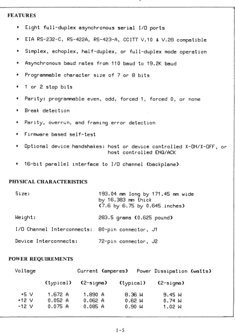
Table 1-1. 27130B MUX Specifications
FEATURES
*
Eight full-duplex asynchronous serial I/O ports*
EIA RS-232-C, RS-422A, RS-423-A, CCITT V.10&
V.28 compatible*
Simplex, echoplex, half-d~plex, or full-duplex mode operation*
Asynchronous baud rates from 110 baud to 19.2K baud*
Programmable character size of 7 or 8 bits*
1 or 2 stop bits*
Parity: programmable even, odd, forced 1, forced 0, or none*
Break detection*
Parity, overrun, and framing error detection*
Firmware based self-test*
Optional device handshakes: host or device controlled X-ON/X-oFF, orhost controlled ENQ/ACK
*
16-bit parallel interface to I/O channel (backplane)PHYSICAL CHARACTERISTICS
Size: 193.04 mm long by 171.45 mm wide
by 16.383 mm thick
(7.6 by 6.75 by 0.645 inches)
W~ight: 283.5 grams (0.625 pound)
I/O Channel Interconnects: 80-pin connector, J1
Device Interconnects: 72-pln connector, J2
PO"'ER REQUIREMENTS
Vol tage Current (amperes) Power Dissipation (watts)
+5 V +12 V
(typical)
1 .672 A
0.052 A
(2-sigma)
1 .890 A
0.062 A
(typical)
8.36 W
0.62
W
(2-sigma)
9.45
W
[image:11.613.73.547.92.766.2]INSTALLATION
1-~
__________________
~[KJ
INTRODUCTION
This section has information for installing and checking the operation of the MUX.
DETERMINING CURRENT REQUIREMENTS
The MUX circuit card obtains its operating voltages from the host computer power supply through the 1/0 channel. Before installing the MUX, it is necessary to determine whether the added current will overload the power supply. The current requirements of the MUX are listed in the power require-ments part of Table 1-1. Current requirerequire-ments for all other I/O cards can be found in the ap-propriate Technica: Reference Manuals.
FIRMW ARE (EPROM) INST ALLA TION
I
CAUTIONI
SOME OF THE COMPONENTS USED IN THIS PRODUCT ARE SUSCEPTIBLE TO DAMAGE BY STATIC DISCHARGE. REFER TO THE SAFETY CONSIDERATIONS INFORMATION AT THE FRONT OF THIS MANUAL BEFORE HANDLING THE CARD OR REMOVING OR REPLACING COMPONENTS.
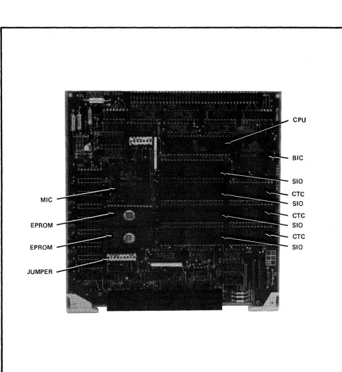
The EPROMs are installed in sockets on the MUX card as shown in Figure 2-1. Be sure that they are installed properly, and that they have not been either damaged or loosened from their sockets during shipping.
CPU
BIC
SID
CTC MIC
SID
CTC
EPROM SID
CTC
EPROM SID
JUMPER
[image:14.618.56.547.98.633.2]JUMPERS
There are two jumpers on the MUX card: a Memory Configuration jumper, and a Signature Analysis jumper. The locations of these two jumpers are shown in Figure 2-1.
Memory Configuration Jumper
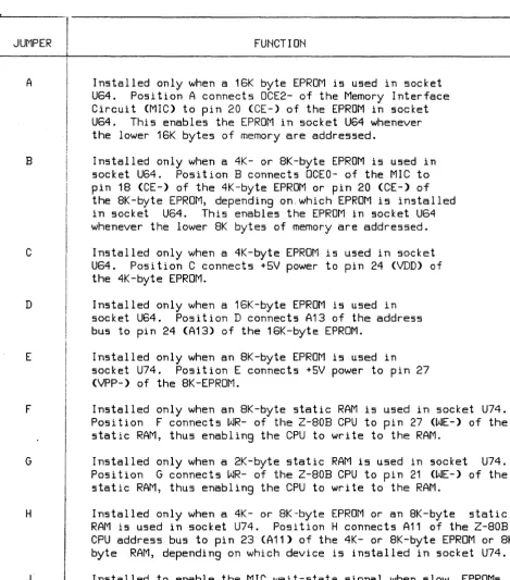
The Memory Configuration jumper, WI, is an internally-connected, 18 pin, dual in-line package (DIP) shunt network. The jumper configures the two memory sockets (U64 and U74) to accomodate dif-ferent kinds of EPROMs and static RAMs The pin diagram of WI is shown in Figure 2- 2; pin func-tions are listed in Table 2-1.
16 17 16 15 14 13 12 11 10
:2 .3 4. 6 7 9
JUMPER
A
B
C
D
E
F
G
H
J
table 2-1. functions of the memory configuration jumper
FUNCTION
Installed only when a 16K byte EPROM is used in socket
U64.
Position A connects OCE2- of the Memory Interface
Circuit (MIC) to pin 20 (CE-) of the EPROM in socket
U64.
This enables the EPROM in socket U64 whenever
the lower 16K bytes of memory are addressed.
Installed only when a 4K- or BK-byte EPROM is used in
socket U64.
Position B connects OCEO- of the MIC to
pin 1B (CE-) of the 4K-byte EPROM or pin 20 (CE-) of
the BK-byte EPROM, depending on. which EPROM is installed
in socket U64.
This enables the EPROM in socket U64
whenever the lower BK bytes of memory are addressed.
Installed only when a 4K-byte EPROM is used in socket
U64.
Position C connects +5V power to pin 24 (VDD) of
the 4K-byte EPROM.
Installed only when a 16K-byte EPROM is used in
socket U64.
Position D connects A13 of the address
bus to pin 24 (A13) of the 16K-byte EPROM.
Installed only when an BK-byte EPROM is used in
socket U74.
Position E connects +5V power to pin 27
(VPP-) of the BK-EPROM.
Installed only when an BK-byte static RAM is used in socket U74.
POSition F connects WR- of the Z-BOB CPU to pin 27 (WE-) of the
static RAM, thus enabling the CPU to write to the RAM.
Installed only when a 2K-byte static RAM is used in socket U74.
Position G connects WR- of the Z-B08 CPU to pin 21 (WE-) of the
static RAM, thus enabling the CPU to write to the RAM.
Installed only when a 4K- or 8K-byte EPROM or an BK-byte static
RAM is used in socket U74.
Position H connects A11 of the Z-BOB
CPU address bus to pin 23 (A11) of the 4K- or BK-byte EPROM or BK
byte RAM, depending on which device is installed in socket U74.
[image:16.615.82.552.93.627.2]Signature Analysis Jumper
The Signature Analysis jumper, U 34, is a 14-pin, pre-programmed shunt network. The internal con-nections of this jumper are set at the factory and are shown in Figure 2- 3 for informatIOn only.
14 13 12 11 10 9 8
4 5 7
Figure 2-3. Signature Analysis 1umper Internal Connections
1/0 CHANNEL INTERFACE
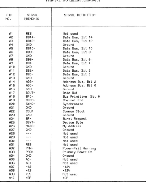
All interface between the MUX and the host computer occurs on the I/O channel. An 80-pin connec-tor (J 1) located on the MUX mates with a receptacle on the
1/0
channel. Connections to 11 are listed in Table 2-2.PERIPHERAL
DEVICE
INTERF ACE
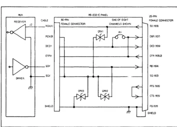
Interface between the MUX card and up to eight peripheral devices is via a 72- pin connector (J2) to an RS-232-C Connection Unit, and from there, via eight separate connectors and eight cables, to the peripheral devices. A connection diagram for the RS- 2 3 2C panel is shown in Figure 2 - 4.
f>,fJX R$-232-C PANEL
25-PlN RECEIVER CABLE 50-PiN ONE OF EIGHT FEMAlE CONNECTOR
J2 _ _ _ RDXlA.) FEMALE CONNECTOR CHANNELS St-kYWN SO (103~ AX
RDX(S) DSR(1071
oeD)' OCD (109)
DTRX DTR (108.2)
sox RD (104)
SGX SG (102)
AT5 (105)
CRX3 CRX2
CTS (105)
SHIELD FG (101)
[image:18.615.128.482.318.571.2]PIN
NO.
A1
A2
A3
A4
AS
A6
A7
AS
A9
A10
A11
A12
A13
A14
A15
A16
A17
A18
A19
A20
A21
A22
A23
A24
A25
A26
A27
A28
A29
A30
A31
A32
A33
A34
A35
A36
A37
A38
A39
A40
SIGNAL
MNEMONIC
RES
DB14-
DB12-GND
DB10-
DB8-GND
DB6-
DB4-GND
DB2-
DBO-GND
AD2-
ADO-GND
DDUT-
BPO-
CEND-
SYNC-GND
CCLK
GND
BR-
DBYT-
MYAD-GND
RES
PFW-PPON
GND
AC-AC+
-12
+12
+5S
+5P
Table 2- 2. I/O Channel Connector J 1
SIGNAL DEFINITION
Not used
Data Bus, Bit 14
Data Bus, Bit 12
Ground
Data Bus, Bit 10
Data Bus, Bi
t8
Ground
Data Bus, Bit
6Data Bus, Bit
4Ground
Data Bus, Bi
t2
Data Bus, Bit 0
Ground
Address Bus, Bi
t2
Address Bus, Bi
t0
Ground
Data Out
Bus Primitive Bit 0
Channel End
Synchronize
Ground
Common Clock
Ground
Burst Request
Device Byte
My
Address
Ground
Not used
Not used
Not used
Not used
Power-Fail Warning
Primary Power On
Ground
[image:19.613.71.543.85.674.2]Table 2-2. I/O Channel Connector 11 (Continued)
PIN
SIGNAL
SIGNAL DEFINITION
NO.
MNEMONIC
I
B1
---
Not used
B2
DB15-
Data Bus,
Bit 15
B3
DB13-
Data Bus, Bi t 13
B4
GND
Ground
I
B5
DB11-
Data Bus, Bi t 11
I
B6
DB9-
Data Bus,
Bit 9
B7
GND
Ground
B8
DB7-
Data Bus,
Bit 7
I
B9
DB5-
Data Bus, Bi t 5
I
B10
GND
Ground
B11
DB3-
Data Bus, Bi t 3
B12
DB1-
Data Bus, Bi t 1
B13
GND
Ground
B14
AD3-
Address Bus,
Bit 3
B15
AD1-
Address Bus, Bi t 1
B16
GND
Ground
B17
UAD-
Unary Address
B18
BP1-
Bus Primitive Bi t 1
I
B19
CBYT-
Channel Byte
B20
POLL-
Poll
I
B21
GND
Ground
IB22
IOSB-
I/O Strobe
B23
GND
Ground
B24
ARQ-
Attention Reguest
B25
DEND-
Device End
I
IB26
IFC-
Interface Clear
I
B27
GND
Ground
I
B28
---
iNot used
I
B29
---
I
Not used
I
B30
B31
RES
ISPU
I
I
Not used
Not used
I
B32
NMI-
INon-Maskable Interrupt
i
B33
SPON
Secondary Power On (NOT USED BY MUX CARD)
i
I
I
B34
B35
GND
AC-
Ground
Not used
B36
AC+
Not used
I
B37
-12
-12V
B38
+12
+12V
B39
+5S
Not used
Table 2-3. Connector 12 Pin Assignments
J2
J2
SID.
J2
J2
SID
PIN NO.
MNEMONIC
MNEMONIC
PIN. NO.
MNEMONIC
MNEMONIC
B25
SDO (A)
TxDO
B4
RDO (A)
RxDO
B26
SGO
B6RDO (B)
B27
SDO (B)
I
A25
SD1 (A)
TxD1
A4
RD1 (A)
RxD1
A26
SG1
B7
RD1 (B)
A27
SD1 (B)
B28
SD2 (A)
TxD2
A6
RD2 (A)
RxD2
B29
SG2
B30
SD2 (B)
B8
RD2 (B)
IA28
SD3 (A)
I
TxD3
A8
RD3 (A)
RxD3
A29
SG3
I
I
A30
SD3 (B)
B9RD3 (B)
B31
SD4 (A)
TxD4
A10
RD4 (A)
RxD4
B32
SG4
II
iB33
SD4 (B)
B10
RD4 (B)
I
A31
SD5 (A)
TxD5
A12
RDS (A)
RxD5
I
A32
SG5
I
A33
SD5 (B)
B11
RDS
(E)I
B34
SD6 (A)
TxD6
A14
RDS (A)
Rx[6
B35
SG6
I
I
B36
SD6 (B)
B12
RD6 (B)
I
!
A34
SD7 (A)
TxD7
B15
RD7 (A)
I
RxD7
A35
SG7
IA36
SD7
(B)B13
RD7 (B)
IA17
SDO
TxDO
A21
SD4
I
TxD4
B17
SCO
I
B21
SC4
I
A18
SD1
TxD1
A22
SDS
TxD5
B18
SC1
B22
SCS
II
I IA19
SD2
TxD2
A23
SDS
TxD6
B19
SC2
B23
SC6
A20
SD3
TxD3
A24
SD7
TxD7
B20
SC3
B24
SC7
A3
HoOD_oN-
CTSAO-
B14
SG
----B3
HLED
- - - -A16
GND
----A2
-12V
----B1
+5V
TO
CONNECTION
BOX
J8
BLU
50-pin connector
17 PAIR DOUBLE-SHIELDED
CABLE (exposed shield connection 50mm from
72-pin connector)
(2) ORN (4) BRN (6) BLU (8) GRN (10) GRY
TO
MUX
J2
(1 2)0
:iliNica-==-~~=
(14) :iiBR~N=--=-~~=
(16) BLU
o
0
Pair #17 not
0
0
connected th is end.
0
0
Extension Cable Fabrication
The 27130B l\1UX is shipped with an extension cable connector kit to help fabrication of an extension cable between the MUX card and the eight-port, RS-232-C connection box.
Note
This extension cable should NOT be longer than 300 feet maximum.
The recommended bulk cable to use for an extension is available from the Hewlett-Packard Parts Center in Mountain View, California under the HP part number: 8120-4510.
Note
Colored and twisted pairs of wires must be carefully identified in the cable. These pairs must be con-nected to specific terminal pins on the connectors for correct cable fabrication. Refer to Figure 2 for a list of which colored pairs of wires are connected to which connector pins.
Use the instruction sheets supplied with the connector kit and the T-tool kit to fabricate your exten-sion cable.
Be careful to match the correct color wire pairs to the correct connector terminal pins on the second connector. Repeat the steps on the sheets to connect the second end of the cable to the second connector.
INST ALLA TION
I
CAUTIONI
AL WAYS ENSURE THA T POWER TO THE COMPUTER IS OFF BEFORE INSER TING OR REMOVING THE MUX CIRCUIT CARD AND CABLE. FAILURE TO DO SO MAY RESULT IN DAMAGE TO THE MUX.
CAUTION
SOME OF THE COMPONENTS USED ON THE PRINTED CIRCUIT CARD ARE SUSCEPTIBLE TO DAMAGE BY STATIC DISCHARGE. REFER TO THE SAFETY CONSIDER A TIONS INFORMATION AT THE FRONT OF THIS MANUAL BEFORE HANDLING THE CARD.
Install the MUX as follows:
EPROMS!RA1\1S are installed in sockets U64 and U74, then refer to Table 2-1 to verify that the correct jumpers are closed.
3. Install the card in the appropriate slot in the computer. Refer to the computer system installation manual to determine the correct slot. \Vhen installing the card, use care not to damage com-ponents and traces on the card and on adjacent cards. Press the1\1UX card firmly into place. 4. Connect the cable supplied with the card from J2 to the RS-232-C panel. If you have the test
hood, which exercises more of the card's circuitry, connect it to J2 instead of connecting the cable. The test hood (HP Part Number 0950-1659) can be ordered from CPC.
I
CAUTIONI
BE SURE TO INSTALL THE DIAGNOSTIC TEST HOOD SO ITS COMPONENT SIDE (THE SIDE WITH THE LED) MATCHES THE COMPONENT SIDE ON THE 1\1UX CARD. DAMAGE TO THE MUX CARD CAN RESULT IF THE COMPONENT SIDES OF THE TWO DEVICES DO NOT MATCH.
Optional Brackets for RS-232C Panel
The optional brackets for the RS-232 panel allow the box to be mounted In the cabinet of the computer.
connection Box Mounting Nuts
Bracket Mounting Screw Holes
Connection Box Mounting Nuts
~
To install bracket in HP model 9030A or 9040A Computer, put hook-tab in slot on side edge of computer and fasten with screws.
Hook-Tab:
Align bracket holes with threaded holes on back of computer.
To install bracket in HP 90S0A Computer, put top tab in an upper side slot of computer cabinet, lift up and put lower tab in lower slot.
NOTE
This bracket needs eight clear side slots in cabinet.
lower Tab
Top Tab
START-UP
To start up and verify correct operation of the l'vfUX, perform the following:
1. Turn on computer system power.
2. A self -test is included on the card. The host computer system determines either if the self -test is run automatically at power-on or if it must be invoked by the user. Refer to the appropriate manual for your system for a description of self-test initiation.
a. If the diagnostic test hood is not installed when the self -test executes, the LED located on the card should light briefly and go out. This indicates that the card passed self -test. If the LED does not light at all, the card may be defective. If the LED stays on, the card did not pass self-test. For either of these latter two cases, we recommend that you return the card to Hewlett-Packard; refer to the next paragraph for reshipment information. If you wish to repair the card, however, refer to Sections V, VI, and VII for maintenance information, replace-able parts lists, and schematic logic diagrams, respectively.
b. If the diagnostic test hood is installed when the self -test executes, the conditions in step l.a. should occur, plus the LED located on the test hood should light briefly and go out. If the LEDs (the one mounted on the card and the one on the diagnostic test hood) do not light at all, or if they light and stay on, the causes are the same as in step 2.a.
3. Refer to your system documentation for information on using the MUX in your system.
RESHIPMENT
If the MUX is to be shipped to Hewlett-Packard for any reason, attach a tag identifying the owner and indicating the reason for shipment. Include the part number of the MUX.
I
D!O
~---~
INTRODUCTION
This section explains how the MUX works or operates.
FUNCTIONAL DESCRIPTION
A functional block diagram of the HP 27130B Eight-Channel Multiplexer is shown in figure 3-1. Reference will also be made to the schematic logic diagram in Section VII, figure 7-1. Note that figure 7-1 consists of five sheets. References to this figure will be as follows: All, 7-1; C23, 7-1; D37, 7-1, etc., where the first digit 0, 2,3,4, or 5) refers to the sheet number; the combination of letters A through E and numbers 11 through 58 (Ail, 037, etc.) refer to the quadrants on the in-dividual sheets; and 7 -1 refers to the figure number. For example,
quadrant quadrant
I I
_1-
-
IA11
D37I I
I
-
sheet I-
sheet 3Circuitry on the MUX card includes a Backplane Interface Circuit (BIC) gate array and its support circuits, a Z- 80B microprocessor (CPU), three Z- 80 Counter Timer Circuits (CTCs), four Z- 80 Serial I/O circuits (510/2s), up to 16K bytes of EPROM in two 28 -pin sockets, a Memory Interface Circuit (MIC) gate array, 64K bytes of dynamic RAM (48K available) R5-422-A/R5-423-A transmitters and receivers (compatible with RS-232-C and CCITT V.28), and I/O channel (backplane) and peripheral device panel (frontplane) connectors.
The heart of the l\'1UX card is the Z-80B CPU (U33, see D24, 7-1), which through a program stored in EPROM controls the functions of the card.
The Backplane Interface Circuit (BIC, U41, see A14, 7-1) is a custom gate array integrated circuit which controls the communication and handshaking with the I/O channel (backplane). The BIC is accessed by the Z-80B CPU as an I/O device for control information, and through Direct Memory Access (OMA) for data transfer to memory.
The Counter Timer Circuits (CTC, U51, U61, and U71, see £43,7-1) divide the system clock to provide baud rate clocks and other necessary clocks for the MUX. They are accessed by the Z-80B CPU as I/O devices.
~
I.IJ ...
... ::>
m
0
~
a.
::a:::
~
-
..J I.IJZ
~
0 0
':::::. .... ...,
SIC
~ 0:: 0
~ ~
Z-808 <:PU
DATA
8
AOOR 16
MIC
Figure 3 -1. MUX Functional Block Diagram LOOP
BM:K
MUX
SERIAL
System Clocks
Three synchronized system clocks (1.8432 MHz, 3.6864 MHz, and 7.3728 MHz), all derived from the 14.7456 MHz clock signal CCLK + (see A21, 7 -1), perform the following functions:
1.8432 MHZ (PHI ___ .CTC): Provides input to the CLK/TRG pins on the CTCs to generate baud rates and system timing intervals.
3.6864 MHz (PHI): Used to provide a system clock to the Z- 80B CPU, the S10s and M1C, and the CTCs.
7.3728 MHz (2 PHI): Drives the MIC.
Memory Address Space
The Z-80B CPU address space of 64K bytes is divided into several sections as shown in figure 3-2. The two memory sockets, U64 and U74, are reserved for EPROMs and/or static RAi\1s. Socket U64 can be configured for 4K, 8K., or 16K byte EPROMs. Socket U74 can be configured for 4K byte EPROM, 8K byte EPROM, 2K byte static RAM, or 8K byte static RAM. Note, however, that when a
16K byte EPROM is installed in U64, socket U74 must be left empty to avoid bus contention.
The address space of U64 is from OH to 3FFFH when this socket is configured for the 16K byte EPROM. The address space is from OH to IFFFH when the socket is configured for 4K or 8K byte EPROMs.
The address space of U74 is fixed between 2000H to 3FFFH. The following types of EPROMs can be installed in socket U64:
4K by 8 (Intel 2732) 8K by 8 (Intel 2764) 16K by 8 (Intel 27128)
The following types of EPROMs and static RAMs can be installed in socket U74: 4K by 8 EPROM (Intel 2732)
8K by 8 EPROM (Intel 2764)
2K by 8 static RAM (Hitachi HM-6116) 8K by 8 static RAM (Hitachi HM -6164)
Memory Configuration jumper WI is used to configure the two memory sockets. WI contains nine~ jumper positions: A, B, C, D, E, F, G, H, and 1. Positions A through D configure socket U64; positions E through H configure U74; and position J enables the WA1T- signal of the MIC to the
z-
80B CPU. The MIC always asserts the WAIT- signal when the lowest 16K byte address is ac-cessed. Position J should be closed (a jumper installed) when EPROMs/RAMs with access times greater than 250 nsec are used. The jumper is shown in Section II, figure 2- 2.NOTE
The 4K by 8 EPROMs and 2K by 8 static RAMs are 24-pin packages and are installed to the back of the sockets (pins 1,2,27, and 28 are not used).
Tables 3-1 and 3-2 show the settings of WI for different types of EPROMs/RAMs.
64K FFFFH
-
-
DFFFH
48K
-
64K-
BFFFH
DYNAMIC RAM
- -
9FFFH
(48K USED)
32K -
-
7FFFH
-
-
5FFFH16K 3FFFH
4K, 8K EPROM
8K 2K, 8K STATIC RAM 1 FFFH
4K, 8K EPROM
OOOOH
MEMORY MAPTable 3 -l. Memory Configuration Jumper (\V I) Settings for Socket U 64
SETTINGS
ADDRESS
SOCKET
SPACE
A
BC
D
U64
COMMENTS
OOOOH-
OPEN
CLOSED
CLOSED
OPEN
4K x 8
OFFFH
Intel
(4K)
2732
OOOOH-
OPEN
CLOSED
DON'T
OPEN
8K x 8
1FFFH
CARE
Intel
(8K)
2764
OOOOH
CLOSED
OPEN
OPEN
CLOSED
16K x 8
Socket
3FFFH
Intel
U74 must
(16K)
27128
be empty
Table 3-2. Memory Configuration Jumper (WI) Settings for Socket U74
SETTINGS
ADDRESS
SOCKET
SPACE
E
F
G HU74
COM'1ENTS
2000H
DON'T
OPEN
OPEN
CLOSED
4K x 8
4K byte
2FFFH
CARE
Intel
EPROM
(4K)
configuration
I
2000H
CLOSED
OPEN
OPEN
CLOSED
8K x 8
8K byte
3FFFH
Intel
EPROM
(8K)
2764
configuration
2000H
OPEN
CLOSED
CLOSED
OPEN
2K x 8
2K byte
27FFH
Hi tachi
static RAM
(2K)
configuration
2000H
OPEN
CLOSED
OPEN
CLOSED
8K x 8
8K byte
3FFFH
Hi tachi
static RAM
1/0
Address Space
The Z-80B CPU provides addressing capability for 256 distinct I/O port registers. The l\1UX card uses only 47 I/O port register addresses: 16 are reserved for the four Z- 80 SIOs, 12 are reserved for the three Z-80 CTCs, 12 are reserved for the MIC, and seven are reserved for the BIC.
Table 3- 3 shows the I/O addresses used by the card.
I
CAUTIONI
THE USE OF ANY OTHER ADDRESSES MAY CAUSE IMPROPER OPERATION.
Z -80B Microprocessor CPU
The
z-
SOB CPU (U33) is an MOS LSI microprocessor which operates from a single + 5-volt supply, uses a single-phase clock, and has a typical instruction execution time of 1 microsecond. The data bus is eight bits wide, and the address bus is 16 bits wide. All CPU pins are TTL compatible.The Z-SOB CPU uses a register-based architecture which includes two sets of six general-purpose registers which can be used as individual S-bit registers or 16-bit register pairs. Additional 8-bit registers include two sets of accumulator and flag registers, and the interrupt vector and mernory refresh registers. Additional 16-bit registers include the stack pointer, program counter, and two index registers. The Z-80B CPU provides the intelligence for the MUX card to function as a preprocessor for the I/O devices, thus relieving the host computer of a considerable amount of processIng.
The functions of the Z-80B CPU signals are shown in table 3-4.
Z -80
S10/2
(Serial
1/0
Controller)
The MUX card uses four Z-80 S10/2 controller circuits (U43, U53, U63, and U73, see A42, 7-1). The Z-80 SIO/2 is a programmable serial I/O controller with two independent full-duplex channels, each of which contains separate control and status lines. Each channel can be indepen-dently programmed. On the MUX card, each of the eight channels is used as a fully programmable asynchronous terminal controller.
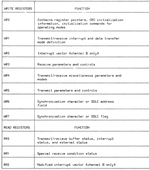
Each SIO channel has two I/O addressable ports: one port for data transfer, and one for control in-formation. Each control port has three read registers and eight write registers available for con-trol information. The functions performed by the registers are shown in table 3-5.
Table 3- 3. I/O Address Space
liD ADDRESS LINES
liD
PORT
liD PORT FUNCTION
7 65
4
3
21
0
ADDR
MIC Register 0
1
1
1
0
0
0
0
0
EO H
MIC Register 1
1
1
1
0
0
0
0
1
E1 H
MIC Register
21
1
1
00
0
1
0
E2 H
MIC Register
31
1
I
1
0
0
0
1
1
E3 H
MIC Register 4
1
1
I
1
0
0
1
0
0
E4 H
MIC Register 5
1
1
I1
0
0
1
0
1
E5 H
I
I
MIC Register
61
1
I
1
0
0
1
1
0
E6 H
MIC Register
7 11
I
1
0
0
1
1
1
E7 H
MIC Register
81
1
1
0
1
0
0
0
E8 H
MIC Register
91
1
I
1
0
1
0
0
1
E9 H
I
MIC Register 10
MIC Register 11
1
1
1
1
I
1
1
0
0
1
1
0
0
1
1
1
0
EA H
EB H
I
eTC 0:
Channel 0
1
1
I
0
1
0
0
0
0
DO H
eTC 0:
Channel 1
1
I1
I0
1
0
0
0
1
D1 H
I
eTC 0:
Channel 2
1
1
0
I
1
0
0
1
0
D2 H
eTC 0:
Channel 3
1
1
I
0
1
0
0
1
1
D3 H
eTC 1 : Channel 0
1
1
I I0
1
0
1
0
0
D4 H
eTC 1: Channel 1
1
1
0
1
0
1
0
1
D5 H
eTC 1 : Channel 2
1
1
0
1
0
I1
1
0
D6H
eTC 1: Channel 3
1
1
0
1
0
1
1
1
D7 H
eTC 2:
Channel 0
1
1
0
1
1
0
0
0
DBH
eTC 2: Channel 1
1
1
I
0
1
1
0
0
1
D9H
eTC 2:
Channel 2
1
1
0
1
1
0
1
0
DA H
eTC 2:
Channel 3
1
1
0
1
1
0
1
1
DB H
!
BIC Register 0
1
0
I
1
1
X0
0
0
BO H
BIC Register 1
10
11
X0
0
1
B1 H
BIC Register
21
0
1
1
X0
1
0
B2 H
BIC Register
31
0
11
X0
1
1
B3 H
BIC Register 4
1
0
1
1
X1
0
0
B4 H
BIC Register 5
1
0
11
X1
0
1
B5 H
BIC Register
61
0
1
1
X1
1
0
B6H
BIC Register
71
0
11
X1
1
1
B7 H
Table 3 - 3. I/O Address Space (Continued)
I/O ADDRESS LINES
I/O
PORT
I/O PORT FUNCTION
7
6
5
4
3
2
1
0
ADDR
SID
0:Channel A Data
0
1 1 10
0
00
70 H
SID
0:Channel A Control
0
1
1 10
0
0 171 H
SID
0:Channel
BData
0
1 1 10
0
1
0
72 H
SID
0:Channel
BControl
0
11
10
0
1
173 H
SID 1 : Channel A Data
0
1
1
1 0 1 00
74 H
SID
1 :Channel A Control
0
1
1 10
1 0 175 H
SID
1 :Channel
BData
0
1
1 10
11
0
76 H
SID 1: Channel
BControl
I0
1
1 10
11
177 H
SID 2: Channel A Data
0
1 1 1 1 I0
00
78 H
SID 2: Channel A Control
0
1 1 1 1 I0 0 1
79 H
SID 2: Channel
BData
0
1 1 1 1I
0
1
0
7A H
SID 2: Channel
BControl
0
1 1 1 1 0 1 17B H
SID 3: Channel A Data
0
I
1 1 1 1
I
1 0 07C H
SID 3: Channel A Control
0
1 1 1 1 1 0 17D H
SID 3: Channel
BDatA
0
I
1 1 1 1 1
1
0
7E H
SIGNAL NAME
AO - A15 (Address Bus)
DO - D7
(Data Bus)
M1-(Machine Cycle 1)
MREQ-(Memory Request)
IORQ-(Input/Output ·Request)
Table 3-4. Z-80B CPU Signals
FUNCTION
Tri-state output, active high.
AO - A15 are a 16-bit address bus (AO is the least significant bit). This bus provides address capability for up to 64K of memory data exchanges, and for I/O device data exchanges.
I/O addressing uses the 8 lower address bits to allow direct addressing of up to 256 input or 256 output ports.
Tri-state input/output, active high.
DO - D7 are an 8-bit bidirectional data bus
used for data exchanges with memory and I/O devices.
Output, active low.
Indicates that the current machine cycle is the OP code fetch cycle of an instruction execution.
Tri-state output, active low.
Indicates that the address bus holds a valid address for a memory read or write.
Tri-state output, active low.
Indicates that the lower half of the address bus holds a valid I/O address for an I/O read
or write. 10RQ- is also generated with
SIGNAL NAME
RD-(Read)
WR-(Write)
RFSH-(Refresh)
HALT-
WAIT-
INT-(Interrupt
Request)
NMI-(Non-Maskable
Interrupt)
Table 3-4. Z-80B CPU Signals (Continued)
FUNCTION
Tri-state output, active low.
Indicates that the CPU wants to read data
from memory or an I/O device.
Memory or
I/O device uses this signal to gate data onto
the CPU data bus.
Tri-state output, active low.
Indicates that the CPU data bus holds valid
data for the addressed memory or I/O device.
Not used by the MUX card.
Not used by the MUX card.
Input, active low.
Indicates to the Z-80B CPU that the addressed
memory or I/O devices are not ready for a
data transfer. This signal allows memory
or I/O devices of any speed to be
synchronized to the Z-80B CPU.
Input, active low.
Generated by I/O devices. A request will be
honored at the end of the current instruction
if an internal Interrupt Enable flip-flop
is enabled and if the BUSRQ- signal is not
active.
SIGNAL NAME
RESET-
BUSRQ-(Bus Request)
BUSAK-(Bus
Acknowledge)
elK
(Clock)
Table 3-4. Z-80B CPU Signals (Continued)
FUNCTION
Input, active low.
Forces the Z-80B CPU program counter to zero
and initializes the Z-80B CPU.
Input, active low.
liD devices and memory use this signal to
request control of the CPU address bus, data
bus, and tri-state control Signals.
Output, active low.
Asserted by the CPU to grant the requesting
device control of the CPU address bus, data
bus, and tri-state control Signals.
Single-phase CMOS level CPU clock input. Maximum
input frequency is 4 MHz.
This clock is driven at
[image:40.620.62.546.112.619.2]Table 3 - 5. SIO Register Functions
WRITE REGISTERS FUNCTION
----.~~
WRO Contains register pOinters, CRC initialization
information, initialization comma.nds for operating modes
WR1 Transmit/receive interrupt and data transfer
mode definition
WR2 Interrupt vector (channel B only>
I
WR3
I
Receive parameters and controls ..I
WR4
I
Transmit/receive mi scellaneous parameters and modes
I
WRS
I
Transmit parameters and controlsI
WR6 Synchronization character or SDLC address
field
I
WR7 Synchronization character or SDLC flag
READ REGISTERS FUNCTION
RRO Transmit/recieve buffer status, interrupt
status, and external status
RR1 Special receive condition status
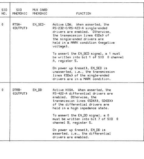
[image:41.615.66.548.104.654.2]SID
NO.
o
I 0
SID
MNEMONIC
RTSA-(OUTPUT)
DTRB-(OUTPUT)
MUX CARD
MNEMONIC
Table 3-6. SIO Special Functions
FUNCTION
Active LOW.
When asserted, the
RS-232-C/RS-423-A single-ended
drivers are enabled.
Otherwise,
the transmission lines (SDs) of
the single-ended drivers are
held in a MARK condition (negative
vol tage).
To assert the EN_SED signal, a 1 must
be written into bit 1 of SIO
0 channel
A, register 5.
On power up (reset), EN_SED is
unasserted, i.e., the transmission
lines (SDs) of the Single-ended
drivers are in a MARK condition.
Active HIGH.
When asserted, the
RS-422-A differential drivers are
enabled. Otherwise, the
transmission lines (SD(A), SD(B»
of the differential drivers are
held in a high impedance state.
To assert the EN_DD Signal. a 0
must be written into bit 7 of SIO
0
channel B, register 5.
[image:42.615.80.555.95.620.2]SID
NO.
SID
MNEMONIC
Table 3-6. SIO Special Functions (Continued)
MUX CARD
MNEMONIC
FUNCTION
1 - - - + - - - · · - - - 1 '
o
1
o
RTSB-(OUTPUT>
RTSB-(OUTPUT>
DTRA-(OUTPUT>
LED
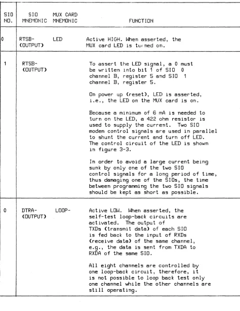
LoOP-Active HIGH. When asserted, the
MUX card LED is turned on.
To assert the LED signal, a 0 must
be written into bit
1of SID
0channel B, register
5and SID
1channel B, register 5.
On power up (reset), LED is asserted,
i.e., the LED on the MUX card is on.
Because a minimum of
6mA is needed to
turn on the LED, a 422 ohm resistor is
used to supply the current. Two SID
modem control signals are used in parallel
to shunt the current and turn off LED.
The control circuit of the LED is shown
in figure
3-3.In order to avoid a large current being
sunk by only one of the two SID
control signals for a long period of time,
thus damaging one of the SIOs, the time
between programming the two SID signals
should be kept as short as possible.
Active LOW.
When asserted, the
self-test loop-back circuits are
activated. The output of
TXDs (transmit data> of each SID
is fed back to the input of RXDs
(receive data> of the same channel,
e.g., the data is sent from TXDA to
RXDA of the same SID.
[image:43.617.80.554.105.718.2]SID
NO.
SID
MNEMONIC
CTSA-(INPUT)
Ta ble 3 - 6. SIO Special Functions (Continued)
MUX CARD
MNEMONIC
FUNCTION
Both the single-ended and differential
drivers should be disabled during the
internal loop back test. This will avoid
unintentional data transmission to the
other systems through the frontplane
drivers, thus causing unpredictable results.
During the internal loop-back test, all
the receivers are automatically disabled.
Thus, the card is completely isolated from
the frontplane receivers.
To assert the LOOP signal, a 1 must be
written into bit 7 of SID 0 channel A,
register 5.
On power up (reset) LOOP- is
unasserted, i.e., no loop back.
If the diagnostic hood is not installed,
the HOOD_ON- signal is pulled to +5V by a
3.3K ohm resistor on the MUX card.
If the diagnostic hood is installed, the
state of HOOD_ON- is the complement of the
state of the HLED- signal (i.e., 0-->1,
1-->0, HLED- --> HOOD-ON-).
Figure 3-4 shows the circuit used to sense
the diagnostic hood.
This circuit is also used
to turn the hood LED on and off.
The state of the HOOD_ON- signal can be read from
bit 5 of SIO
0 channel 1, register O.
A 0
indicates that HOOD_ON- is being pulled to +5V.
A 1 indicates that HOOD_DN- is being pulled to
ground.
[image:44.617.68.546.94.702.2]SID
NO.
o
o
Table 3-6. SIO Special Functions (Continued)
SID
MNEMONIC
MUX CARD
MNEMONIC
RDYA-
DMA2-(OUTPUT)
RDYB-
DMAO-(OUTPUT)
FUNCTION
On power up (reset), if the diagnostic hood is
installed, the HDOD_ON- signal will be pulled to
ground.
If the diagnostic hood is not installed,
the HODD_DN- signal will be pulled to +5V.
Active LOW.
DMA2- is tied to the
IRQ2- input of the MIC.
When
is programmed as
RDYA-(READY-), it is a DMA handshake
Signal. To the MIC's DMA
controller, DMA2- indicates that
channel A of SID 0 is ready to
transfer data to or from memory.
By
using the MIC's DMA capability,
channel A of SID 0 (channel 0 of
the MUX card) can support very high
data rates.
On power up (reset) DMAO- is floating.
Active LOW.
DMAO- is tied to the
IRQO- input of the MIC.
When
is programmed as
RDYB-(READY-), it is a DMA handshake
Signal. To the MIC's DMA
controller, DMAO- indicates that
channel B of SID 0 is ready to
transfer data to or from memory.
By
using the MIC's DMA capability,
channel B of SID 0 (channel 1 of
the MUX card) can support very high
data rates.
[image:45.613.64.553.105.672.2]Table 3-6. SIO Special Functions (Continued)
SID
SID
MUX CARD
NO.
MNEMONIC
MNEMONIC
FUNCTION
1
DTRB-
HLED-
Active LOW.
When asserted, the LED on
(OUTPUT)
the diagnostic hood is on.
To assert the HLED- signal, a 1 must be
be written into bit 7 of SID 1 channel
B,
register 5.
On power up (reset), HLED- is unasserted, i.e. ,
the LED on the diagnostic hood is off.
No modem control lines or modem status inputs are used.
SIO #0
422
RTSB ,.. +5\1
'"
LED
SIO #1
RSTB-V
ON-BOARD lEDI
GNDo
[image:46.613.148.467.380.631.2]SIO #1 SIO
#0
DTRB- HLED-
CTSA-3.3~;
A A +5V
M
yS05
HLED
HOOO_ON-UX CARD
DIAGNOSTIC HOOD
220
+5V
HOOD LED
220
GND
[image:47.613.91.523.110.502.2]CTC (Counter Timer Circuit)
Three Z - 8 0 CTC circuits (U 5 1, lJ 61, U 71, see E 43, 7 -1) are used by the MUX card to provide baud rate and real-time clocks.
The Z- 80 CTC circuit provides four independent counter/timer channels. Three of these timers can supply outputs for other devices; the fourth channel can only cause an interrupt to the Z-80B CPU.
Only the first CTC (CTC 0, U 51) is tied to the MUX card's daisy-chain interrupt structure and is able to generate an interrupt to the Z-80B
cpu.
The fourth timer of CTC 0 is the real-time clock for the card's firmware.CTC 1 (U61) and CTC 2 (U71) are not tied to the interrupt daisy chain, and they are not allowed to generate interrupts. These two CTCs are only used to generate baud rates.
The reason for ~liminating CTC 1 and CTC 2 from the daisy-chain interrupt structure IS to
con-form to the timing requirements of the Z-80B
cpu
during lACK and RETI cycles. See the "Wait State Circuit for Interrupt Acknowledge" paragraph for a timing analysis of the lACK and RETI cycles.The inputs of all four clock triggers (CLK/TRGO through CLK/TRG3) of all three CTCs are driven by the 1. 84 3 2 MHz clock (PHI_ CTC clock, generated by U24, see A2l, 7-1).
The functions of the CTC timer outputs are shown in table 3-7.
Note that the CTCs are I/O addressable ports to the Z-80B CPU; their addresses are defined In table 3- 3.
Interfacing to the BIC
The Backplane Interface Circuit (BIC, see A 14, 7 -1) provides the half -duplex data path to the I/O channel (backplane). As used by the MUX card, the BIC is addressed as an I/O port by the Z- 8 OB CPU (the same as the Z-80 SIO and CTC circuits). In other words,.to read or write from the BIC registers, an IN or OUT instruction is executed to the I/O address of that register. The address space of the BIC is described in table 3- 3.
Data can also be transferred between the BIC and memory directly under control of DMA chan-nel B of the Memory Interface Circuit (MIC).
The BIC is not directly connected to the interrupt daisy chain structure of the MUX card. Instead, the BIC's BINT- (interrupt output, see £14, 7-1) signal is connected to the MIC's IINT- (in-terrupt input, see C31,7 -1) signal. When the MIC is programmed for external interrupt (from the RIC), the MIC will generate an interrupt for the BIC. The MIC also provides an interrupt vector for the BIC when the Z- 80B CPU acknowledges.
Table 3-7. eTC Timer Outputs
TIMER
DRIVEN DEVICE
CTC
CTC
OUTPUT
INPUT
NO.
CH.
MNEMONIC
MNEMONIC
FUNCTION
0 0
IRQH
IRQH of MIC
Reguest hold-off for DMA
0
1
BRG1
SID 0
MUX card channel 1
baud-RXCB-
&TXCB-
rate clock
0 2
BRGO
SID 0
MUX card channel
o
baud-RXCA-
&TXCA-
rate clock
0
3INTERNAL
Cause zero
Real-time clock for
count interrupt firmNare
to Z-80B CPU
1
0
BRG2
SID 1
MUX card channel 2
baud-RXCA-
&TXCA-
rate clock
1
1
BRG3
SID 1
MUX card channel 3
baud-RXCB-
&TXCB-
rate clock
1
2BRG4
SID 2
MUX card channel 4
baud-RXCA-
&TXCA-
rate clock
1
3Not available
Counter value can be
[image:49.615.70.547.101.560.2]Table 3-7. eTC Timer Outputs (Continued)
TIMER
DRIVEN DEVICE
CTC
CTC
OUTPUT
INPUT
NO.
CH.
MNEMONIC
MNEMONIC
FUNCTION
2
0
BRGS
SID 2
MUX card channel S
baud-RXCB- & TXCB-
rate clock
2
1BRG6
SID 3
MUX card channel 6
baud-RXCA- & TXCA-
rate clock
2
2ERG?
SID 3
MUX card channel 7
baud-RXCB- & TXCB-
rate clock
2
3
Not available
Counter value can be
[image:50.615.79.555.98.370.2]PIN
SIGNAL
NO.
MNEMONIC
1 2
3
4 5 6 7 8 910
11 1213
1415
16 1718
1920
21 22 23 2425
2627
28
2930
31
3233
DO
D2
D4 D6END-AO
A1
WR-
RDY-GND
BINT-NMI
IFC
POLL-
SYNCj1YAD-DoUT
BPOUAD
ADO
AD2
CEND
DBO-
DB1-
DB3-
DBS-
DB7-
DB9-
DB10-
DB11-
DB13-
DB15-BR
Table 3- 8. BIC Chip Pin Connections
BIC
MNEMONIC
DO
D2
D4 D6END-AO
A2
DSO-
RDY-
AS-
DTACK-
INT-NMI
IFC
POLL-SYNC_MY
AD-DOUT
BPO
UAD
ADO
AD2
CEND
BIODO-
BIOD1-
BIOD3-
BIODS-
BIOD7-
BIOOO-
BIOD10-
BIOD11-
BIOD13-
BIOD1S-BR
DESCRIPTION
Data Bus, Bit 0
Data Bus, Bit
2Data Bus, Bit 4
Data Bus, Bit
6Indicates end of data read or
write
Register Address, Bit 0
Register Address, Bit
2Z-80B Write
Asserted by BIC when ready for
data transfer
Not used
Not used
BIC Interrupt
Non-Maskable Interrupt
Interface Clear
Poll
In conjunction with DE, determines
data bus drivers mode of operation
Data Out, specifies data bus
direction
Bus Primitive, Bit O.
With BP1,
specifies bus primitive operation
Unary Address, latches BIC channel
address after a PPoN or IFC
Address Bus, Bit 0
Address Bus, Bit
2Channel End
Backplane I/O Data, Bit 0
Backplane I/O Data, Bit 1
Backplane I/O Data, Bit 3
Backplane I/O Data, Bit 5
Backplane I/O Data, Bit 7
Backplane I/O Data, Bit 9
Backplane I/O Data, Bit 10
Backplane I/O Data, Bit 11
Backplane I/O Data, Bit· 13
Backplane I/O Data, Bit 15
Table 3 - 8. BIC Chip Pin Connections (Continued)
PIN
SIGNAL
BIC
NO.
'MNEMONIC
MNEMONIC
34 35
36
37
38
3940
41
42
43 4445
46
47
48
49 50 51 52 53 54 55 56 57 58 5960
61
62
63
64
DBYT
IoSB
D1
D3 D5D7
GND
A1