Future MOSFET Devices using high-k (TiO
2
) dielectric
Prerna
Guru Jambheshwar University, G.J.U.S. & T., Hisar, Haryana, India, [email protected]
Abstract: In this paper, an 80nm NMOS with high-k (TiO2) was designed and fabricated to study its electrical characteristics. ATHENA & ATLAS
module of SILVACO software are used in simulating the electrical performance of the transistor. The parameters under simulation were the threshold voltage (Vt), Id-Vg& Id-VdCharacteristics. High-k gate technology is a strong alternative for replacing the conventional SiO2gates in MOSFETs for
both high performance and low power applications. High-k oxides offer a solution to leakage problems that occurs as the gate oxide thickness is scaled down. Non-ideal effects such as short channel effects mainly channel modulation and drain induced barrier lowering (DIBL) are investigated in it. It is observed in the results that the threshold voltage could be varied by changing the above mentioned device parameters. The effectiveness is also observed on performance parameters of the MOSFET such as drain induced barrier lowering, sub-threshold slope and threshold voltage. Hence device engineering would play an important role in optimizing the device parameters.
Keywords: MOSFET, SCE-short channel effect, High-k, DIBL-drain induced barrier lowering.
1. INTRODUCTION
Since the advent of MOS devices over 40 years ago, SiO2has been
used as an efficient gate dielectric. The need for increased speed at constant power density has led to shrinking of MOSFET dimensions and as per scaling rules; the oxide thickness is also reduced in step. With scaling reaching sub nanometer technology nodes, the introduction of novel materials became inevitable as scaling of SiO2
raises a serious concern in terms of tunneling current and oxide breakdown [7].
In order to prevent direct gate tunneling in very thin oxides, the SiO2 is replaced by alternative materials with higher permittivity and greater physical thickness. However, the introduction of these high-k dielectrics posses several problems, such as bi-dimensional electrostatic effects which may have a dramatic impact on the device performances when the gate dielectric thickness becomes comparable to the device gate length [7].
In this paper section 1.1 contains a description about High-k dielectric (TiO2) while section 2 describes the design and simulation
of N-channel MOSFET device with all the results and analysis discussed in section 3.
1.1 Titanium Dioxide (TiO2) as gate dielectric.
TiO2 has been used as an alternative gate dielectric material for
deep submicron MOSFET’s earlier in 1995 [2]. Advantages: The dielectric constant of TiO2is 80. The bandgap of the material is 3.5eV
for amorphous films and 3.2eV for crystalline films. These band gaps are good for semiconductor but higher bandgap is required to act as an effective insulator [2].
The TiO2has low energy band offset with respect to Si. TiO2has
EOT of less than 10Å. Transistors made with TiO2shows near ideal
behavior but they have challenges with mobility. It has been shown that the low field effective mobility is approximately 160cm2/V-s, which is about a three order lower than the mobility in SiO2based MOSFET’s. This mobility reduction is due to interface trap state and
surface roughness at TiO2/Si interface. The electron traps in TiO2is
due to oxygen vacancy. An empirical relationship between the effective mobility and the interface state density which is given by [2],
μ
μ = ∝ (1)
where Dit is the concentration of charged states at the bias condition and α is a constant. So the effective mobility is inversely
related with Dit[2].
In Si/SiO2interface bond strain causes fixed charge which is about
0.1% of the interface atoms (1010-1011cm2). So for strained-Si/TiO2
leakage occurs from these defects as well as from low conduction band discontinuity. Therefore, ultra-thin SiO2 can be incorporated
between TiO2and strained-Si layer to reduce the defect states at the
interface. Therefore if TiO2 is grown on (100) Si substrate Dit
decreases and the mobility increases [2]. Mobility also can be increased by growing TiO2gate dielectric stack on Si substrate. The
device speed can be improved by 20-80% at a constant gate length by using high mobility strained-Si at the channel region. TiO2reduces
gate leakage and Si enhances the device speed [2]. Hence TiO2is our
choice of high-k dielectric gate material. The other high-k materials are shown in table-1 [2] with their properties along with TiO2.
Table 1: High-k dielectric materials and their properties. Gate
dielectric
Material
Dielectric
constant
(k)
Energy
bandgap
Eg (eV)
Conduction
band offset
∆Ec (eV)
Valence
band
offset
∆Ec(eV)
SiO2 3.9 9 3.5 4.4
Al2O3 8 8.8 3 4.7
www.ijraset.com
Vol. 1 Issue II, September2013
ISSN: 2321-9653
I N T E R N A T I O N A L J O U R N A L F O R R E S E A R C H I N A P P L I E D S C I E N C E A N D E
N G I N E E R I N G T E C H N O L O G Y (I J R A S E T)
ZrO2 25 5.8 1.4 3.3
HfO2 25 5.8 1.4 3.3
Ta2O5 25 6 1.5 3.4
Y2O3 13 6 2.3 2.6
Ya2O3 27 4.3 2.3 0.9
2. DESIGN & SIMULATION
Simulations are performed with a two-dimensional (2-D) device simulator, SILVACO. The physical structure of the high-k NMOS used in our present study are designed using ATHENA considering the standard Silicon Integrated chip processing technology and the electrical characteristics are simulated using ATLAS device simulator.
The specifications of the Silicon substrate considered for the design are p-type Boron doped substrate with doping concentration of 1 x 10¹⁸ atoms cm-3 and <100> orientation. The design structure consists of TiO2 dielectric with Polysilicon gate is considered to
explore the advantages of TiO2over SiO2dielectric. The simulated
structure, which are based on fully scaled 80 nm gate length
MOSFET’s proposed in the ITRS, have gate length of 80 nm, with effective oxide thicknesses (EOT) of 2nm [4]. The dielectric constant of TiO2 gate dielectric was considered to be 80. Steep retrograde
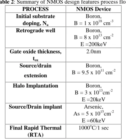
channel doping is used with surface doping concentration of 8 x 1013 cm-3. The complete summary of NMOS process flow is given below in table 2.
Table 2: Summary of NMOS design features process flow.
PROCESS NMOS Device
Initial substrate doping, Na
Boron, B = 1 x 1018cm-3
Retrograde well Boron,
B = 8 x 1013cm-2 E =200keV
Gate oxide thickness, tox
2.0nm
Source/drain
extension
Boron, B = 9.5 x 1011cm-2
Halo Implantation Boron,
B = 3 x 1013cm-2 E =20keV
Source/Drain implant Arsenic, As = 5 x 1015cm-2
E =60keV
Final Rapid Thermal (RTA)
1000oC/1 sec
3. RESULTS & DISCUSSION.
The results of fabrication & simulation of 80nm NMOS can be viewed in the TONYPLOT is as shown below. Figure1 shows the electrodes are highlighted in this final structure of this NMOS device.
The complete structure now can be simulated in ATLAS to provide specific characteristics such as Id-Vg& Id-Vdcurve.
[image:3.595.334.550.197.354.2]The simulated device structure (figure 1) is a symmetric N-channel NMOS with following parameters mentioned in table 3.
[image:3.595.336.542.415.589.2]FIGURE 1 : COMPLETE STRUCTURE OF 80NM NMOS WITH TIO2.
Table 3: Device parameters taken for process simulation of device
design using ATHENA simulation tool.
PARAMETERS NMOS
Sheet Resistance
(Ω/square)
1624.31
Channel Surface Concentration (atoms/cm3)
5.34893x 10¹⁷
Gate oxide thickness,
tox(nm)
2.0
Gate Length, L(µm) .08
Gate Width, W(µm) .2
Channel Length (µm) .04
Channel Width (µm) .3
The simulated NMOS structure with source/drain junction depth and net doping concentration is shown below in figure 2.
www.ijraset.com
Vol. 1 Issue II, September2013
ISSN: 2321-9653
I N T E R N A T I O N A L J O U R N A L F O R R E S E A R C H I N A P P L I E D S C I E N C E A N D E
N G I N E E R I N G T E C H N O L O G Y (I J R A S E T)
ZrO2 25 5.8 1.4 3.3
HfO2 25 5.8 1.4 3.3
Ta2O5 25 6 1.5 3.4
Y2O3 13 6 2.3 2.6
Ya2O3 27 4.3 2.3 0.9
2. DESIGN & SIMULATION
Simulations are performed with a two-dimensional (2-D) device simulator, SILVACO. The physical structure of the high-k NMOS used in our present study are designed using ATHENA considering the standard Silicon Integrated chip processing technology and the electrical characteristics are simulated using ATLAS device simulator.
The specifications of the Silicon substrate considered for the design are p-type Boron doped substrate with doping concentration of 1 x 10¹⁸ atoms cm-3 and <100> orientation. The design structure consists of TiO2 dielectric with Polysilicon gate is considered to
explore the advantages of TiO2over SiO2dielectric. The simulated
structure, which are based on fully scaled 80 nm gate length
MOSFET’s proposed in the ITRS, have gate length of 80 nm, with effective oxide thicknesses (EOT) of 2nm [4]. The dielectric constant of TiO2 gate dielectric was considered to be 80. Steep retrograde
channel doping is used with surface doping concentration of 8 x 1013 cm-3. The complete summary of NMOS process flow is given below in table 2.
Table 2: Summary of NMOS design features process flow.
PROCESS NMOS Device
Initial substrate doping, Na
Boron, B = 1 x 1018cm-3
Retrograde well Boron,
B = 8 x 1013cm-2 E =200keV
Gate oxide thickness, tox
2.0nm
Source/drain
extension
Boron, B = 9.5 x 1011cm-2
Halo Implantation Boron,
B = 3 x 1013cm-2 E =20keV
Source/Drain implant Arsenic, As = 5 x 1015cm-2
E =60keV
Final Rapid Thermal (RTA)
1000oC/1 sec
3. RESULTS & DISCUSSION.
The results of fabrication & simulation of 80nm NMOS can be viewed in the TONYPLOT is as shown below. Figure1 shows the electrodes are highlighted in this final structure of this NMOS device.
The complete structure now can be simulated in ATLAS to provide specific characteristics such as Id-Vg& Id-Vdcurve.
The simulated device structure (figure 1) is a symmetric N-channel NMOS with following parameters mentioned in table 3.
FIGURE 1 : COMPLETE STRUCTURE OF 80NM NMOS WITH TIO2.
Table 3: Device parameters taken for process simulation of device
design using ATHENA simulation tool.
PARAMETERS NMOS
Sheet Resistance
(Ω/square)
1624.31
Channel Surface Concentration (atoms/cm3)
5.34893x 10¹⁷
Gate oxide thickness,
tox(nm)
2.0
Gate Length, L(µm) .08
Gate Width, W(µm) .2
Channel Length (µm) .04
Channel Width (µm) .3
[image:3.595.58.267.476.708.2]FIGURE 2 : NMOS STRUCTURE SHOWING THE JUNCTION DEPTH.
The complete structure can now be simulated using ATLAS to provide specific characteristics such as Id-Vg, Id-Vd, sub-threshold and
DIBL curve.
Figure 3 shows that Idvs. Vgcurve, which gives the extraction of
threshold voltage. The threshold voltage of this operation happens when the current reaches zero. Vd= -0.1V is applied for this graph.
When Vg<Vt, the current is zero but the current start increasing when
Vg>Vt. With a small value of Vdapplied it is possible to examine the
effect of an increase gate voltage. After reaching the threshold voltage the induced n-channel begins to increase in depth. The name enhancement type is tacked onto this type of MOSFET as a result of the gate voltage having to overcome the threshold voltage & enhance the channel [3].
FIGURE 3 : THE IDVS. VGCURVE.
Figure 4 shows the families of Idvs. Vdcurves for NMOS. This
curve is plotted using ATLAS simulator. The gate voltages that apply for 50.5V, 100.5V, & 150.5V denoted by red, green & blue lines [3]. The graph in figure 4 shows Id-Vd not saturated due to the punch
through effect only for Punch through causes a rapidly increasing current with increasing drain-source voltage. It is an extreme cause of channel length modulation where the depletion layers around the drain & source region merge into single depletion region. Suppose the red, green & blue line in graph start saturate at 0.2515V, 0.2517V & 0.2519V. But, this graph not saturate due to punch through effect [3].
FIGURE 4 : THE ID VS. VD CURVE.
Figure 5 shows the sub-threshold characteristic curve for NMOS device with TiO2as gate dielectric. Sub-threshold characteristic of a
MOSFET is an important parameter which determines the holding time in dynamic circuits as well as the static power dissipation in static CMOS circuits [5]. The sub-threshold current is due to weak inversion in the channel between flat-band and threshold voltage (for band-bending between zero and 2φF), which leads to a diffusion
current from source to drain [6].
Figure 5 : Sub-threshold characteristic.
If small channel length MOSFETs are not scaled properly and the source/drain junctions are too deep or the channel doping is too low, there can be unintended electrostatic interactions between the source and the drain known as Drain Induced Barrier Lowering (DIBL). This leads to punch-through leakage or breakdown between the source and the drain, and loss of gate control [6]. A DIBL test is performed for the transistor, which results in a Id-Vg plotted at different drain
voltages (Vd). Figure 6 shows a decreasing DIBL curve for NMOS
transistor with 0.025V and 0.05V drain voltage are shown by green & red curves respectively.
FIGURE 2 : NMOS STRUCTURE SHOWING THE JUNCTION DEPTH.
The complete structure can now be simulated using ATLAS to provide specific characteristics such as Id-Vg, Id-Vd, sub-threshold and
DIBL curve.
Figure 3 shows that Idvs. Vgcurve, which gives the extraction of
threshold voltage. The threshold voltage of this operation happens when the current reaches zero. Vd= -0.1V is applied for this graph.
When Vg<Vt, the current is zero but the current start increasing when
Vg>Vt. With a small value of Vdapplied it is possible to examine the
effect of an increase gate voltage. After reaching the threshold voltage the induced n-channel begins to increase in depth. The name enhancement type is tacked onto this type of MOSFET as a result of the gate voltage having to overcome the threshold voltage & enhance the channel [3].
FIGURE 3 : THE IDVS. VGCURVE.
Figure 4 shows the families of Idvs. Vdcurves for NMOS. This
curve is plotted using ATLAS simulator. The gate voltages that apply for 50.5V, 100.5V, & 150.5V denoted by red, green & blue lines [3]. The graph in figure 4 shows Id-Vd not saturated due to the punch
through effect only for Punch through causes a rapidly increasing current with increasing drain-source voltage. It is an extreme cause of channel length modulation where the depletion layers around the drain & source region merge into single depletion region. Suppose the red, green & blue line in graph start saturate at 0.2515V, 0.2517V & 0.2519V. But, this graph not saturate due to punch through effect [3].
FIGURE 4 : THE ID VS. VD CURVE.
Figure 5 shows the sub-threshold characteristic curve for NMOS device with TiO2as gate dielectric. Sub-threshold characteristic of a
MOSFET is an important parameter which determines the holding time in dynamic circuits as well as the static power dissipation in static CMOS circuits [5]. The sub-threshold current is due to weak inversion in the channel between flat-band and threshold voltage (for band-bending between zero and 2φF), which leads to a diffusion
current from source to drain [6].
Figure 5 : Sub-threshold characteristic.
If small channel length MOSFETs are not scaled properly and the source/drain junctions are too deep or the channel doping is too low, there can be unintended electrostatic interactions between the source and the drain known as Drain Induced Barrier Lowering (DIBL). This leads to punch-through leakage or breakdown between the source and the drain, and loss of gate control [6]. A DIBL test is performed for the transistor, which results in a Id-Vg plotted at different drain
voltages (Vd). Figure 6 shows a decreasing DIBL curve for NMOS
www.ijraset.com
Vol. 1 Issue II, September2013
ISSN: 2321-9653
I N T E R N A T I O N A L J O U R N A L F O R R E S E A R C H I N A P P L I E D S C I E N C E A N D E
N G I N E E R I N G T E C H N O L O G Y (I J R A S E T)
Figure 6 : DIBL curve.
3.1 Effect of drain voltage on threshold voltage
The value of gate to source voltage (Vgs) for which sufficient
amount of mobile electrons accumulates in the channel region so that a conducting channel is formed is called the threshold voltage [7].
The Figure 7 describes the effect of drain voltage on threshold voltage for NMOS with TiO2gate dielectric. It is observed from the
analysis that as the drain voltage increases, the threshold voltage decreases for NMOS. Thus, the threshold voltage of the device could be varied by applying different drain voltage to the transistor. However, a reduction in the threshold voltage gives rise to an increase in the sub-threshold leakage current, which is the current that is conducted through a transistor from its source to drain when the device is intended to be off. Due to this increase in sub-threshold current, static power consumption is increased and the overall device performance is degraded [1].
Figure 7 : Effect of drain voltage on threshold voltage.
An increase in threshold voltage is observed if the drain voltage applied to the transistor is quite low in magnitude, with an accompanying decrease in off state leakage current. Increasing the threshold voltage of the NMOS is an effective way to reduce sub-threshold leakage.
3.2 EFFEC T O F GATE OXIDE THIC KNESS ON THR ESHOLD VOLTAGE
Figure 8 shows effect of gate oxide thickness on threshold voltage by varying the gate oxide thickness from 2.0nm to 3.5nm. The gate oxide thickness was the first parameter that was modified. The value of gate oxide thickness was modified to get the gate oxide thickness value in line with ITRS guideline for 80nm device [2].
With Increase in gate oxide thickness, Vtincreases. The gate oxide
thickness is a reverse proportion to the gate capacitance. When the gate oxide capacitance goes down, which means that the gate has less control over the channel in order to invert the channel, the Vt will
increase.
Figure 8 : Effect of gate oxide thickness on threshold voltage.
3.3 EFFEC T OF GATE OXIDE THIC KNESS ON SHEET RESISTANC E.
Sheet resistance is a measure of resistance of thin films that are nominally uniform in thickness. It is commonly used to characterize materials made by semiconductor doping, metal deposition etc. Examples of these processes are: doped semiconductor region (e.g., silicon or polysilicon).This parameter is applicable to dimensional systems in which thin films are considered as two-dimensional entities. This term implies that current flow is along the plane of the sheet, not perpendicular to it. Figure 9 shows effect of gate oxide thickness on Sheet resistance. With Increase in gate oxide thickness, sheet resistance decreases.
-0.8 -0.75-0.7 -0.65-0.6 -0.55
-1.5 -1 -0.5
T h re sh o ld V o lt a g e (V )
Drain Bias (V)
Threshold Voltage vs Drain
Voltage
www.ijraset.com
Vol. 1 Issue II, September2013
ISSN: 2321-9653
I N T E R N A T I O N A L J O U R N A L F O R R E S E A R C H I N A P P L I E D S C I E N C E A N D E
N G I N E E R I N G T E C H N O L O G Y (I J R A S E T)
Figure 6 : DIBL curve.
3.1 Effect of drain voltage on threshold voltage
The value of gate to source voltage (Vgs) for which sufficient
amount of mobile electrons accumulates in the channel region so that a conducting channel is formed is called the threshold voltage [7].
The Figure 7 describes the effect of drain voltage on threshold voltage for NMOS with TiO2gate dielectric. It is observed from the
analysis that as the drain voltage increases, the threshold voltage decreases for NMOS. Thus, the threshold voltage of the device could be varied by applying different drain voltage to the transistor. However, a reduction in the threshold voltage gives rise to an increase in the sub-threshold leakage current, which is the current that is conducted through a transistor from its source to drain when the device is intended to be off. Due to this increase in sub-threshold current, static power consumption is increased and the overall device performance is degraded [1].
Figure 7 : Effect of drain voltage on threshold voltage.
An increase in threshold voltage is observed if the drain voltage applied to the transistor is quite low in magnitude, with an accompanying decrease in off state leakage current. Increasing the threshold voltage of the NMOS is an effective way to reduce sub-threshold leakage.
3.2 EFFEC T O F GATE OXIDE THIC KNESS ON THR ESHOLD VOLTAGE
Figure 8 shows effect of gate oxide thickness on threshold voltage by varying the gate oxide thickness from 2.0nm to 3.5nm. The gate oxide thickness was the first parameter that was modified. The value of gate oxide thickness was modified to get the gate oxide thickness value in line with ITRS guideline for 80nm device [2].
With Increase in gate oxide thickness, Vtincreases. The gate oxide
thickness is a reverse proportion to the gate capacitance. When the gate oxide capacitance goes down, which means that the gate has less control over the channel in order to invert the channel, the Vtwill
increase.
Figure 8 : Effect of gate oxide thickness on threshold voltage.
3.3 EFFEC T OF GATE OXIDE THIC KNESS ON SHEET RESISTANC E.
Sheet resistance is a measure of resistance of thin films that are nominally uniform in thickness. It is commonly used to characterize materials made by semiconductor doping, metal deposition etc. Examples of these processes are: doped semiconductor region (e.g., silicon or polysilicon).This parameter is applicable to dimensional systems in which thin films are considered as two-dimensional entities. This term implies that current flow is along the plane of the sheet, not perpendicular to it. Figure 9 shows effect of gate oxide thickness on Sheet resistance. With Increase in gate oxide thickness, sheet resistance decreases.
-0.5 -0.1
Drain Bias (V)
Threshold Voltage vs Drain
Voltage
-0.8 -0.7 -0.6 -0.5 2 2.2 T h re sh o ld V o lt a g e (V )Gate oxide thickness (nm)
Gate oxide thickness vs
Threshold voltage
1624.24 1624.26 1624.28 1624.3 1624.32 2 S h ee t R esi st a n ce ( Ω / sq u a re )Gate oxide thickness (nm)
Gate oxide thickness vs Sheet
Resistance
www.ijraset.com
Vol. 1 Issue II, September2013
ISSN: 2321-9653
I N T E R N A T I O N A L J O U R N A L F O R R E S E A R C H I N A P P L I E D S C I E N C E A N D E
N G I N E E R I N G T E C H N O L O G Y (I J R A S E T)
Figure 6 : DIBL curve.
3.1 Effect of drain voltage on threshold voltage
The value of gate to source voltage (Vgs) for which sufficient
amount of mobile electrons accumulates in the channel region so that a conducting channel is formed is called the threshold voltage [7].
The Figure 7 describes the effect of drain voltage on threshold voltage for NMOS with TiO2gate dielectric. It is observed from the
analysis that as the drain voltage increases, the threshold voltage decreases for NMOS. Thus, the threshold voltage of the device could be varied by applying different drain voltage to the transistor. However, a reduction in the threshold voltage gives rise to an increase in the sub-threshold leakage current, which is the current that is conducted through a transistor from its source to drain when the device is intended to be off. Due to this increase in sub-threshold current, static power consumption is increased and the overall device performance is degraded [1].
Figure 7 : Effect of drain voltage on threshold voltage.
An increase in threshold voltage is observed if the drain voltage applied to the transistor is quite low in magnitude, with an accompanying decrease in off state leakage current. Increasing the threshold voltage of the NMOS is an effective way to reduce sub-threshold leakage.
3.2 EFFEC T O F GATE OXIDE THIC KNESS ON THR ESHOLD VOLTAGE
Figure 8 shows effect of gate oxide thickness on threshold voltage by varying the gate oxide thickness from 2.0nm to 3.5nm. The gate oxide thickness was the first parameter that was modified. The value of gate oxide thickness was modified to get the gate oxide thickness value in line with ITRS guideline for 80nm device [2].
With Increase in gate oxide thickness, Vtincreases. The gate oxide
thickness is a reverse proportion to the gate capacitance. When the gate oxide capacitance goes down, which means that the gate has less control over the channel in order to invert the channel, the Vtwill
increase.
Figure 8 : Effect of gate oxide thickness on threshold voltage.
3.3 EFFEC T OF GATE OXIDE THIC KNESS ON SHEET RESISTANC E.
Sheet resistance is a measure of resistance of thin films that are nominally uniform in thickness. It is commonly used to characterize materials made by semiconductor doping, metal deposition etc. Examples of these processes are: doped semiconductor region (e.g., silicon or polysilicon).This parameter is applicable to dimensional systems in which thin films are considered as two-dimensional entities. This term implies that current flow is along the plane of the sheet, not perpendicular to it. Figure 9 shows effect of gate oxide thickness on Sheet resistance. With Increase in gate oxide thickness, sheet resistance decreases.
2.2 2.5 3.3 3.5
Gate oxide thickness (nm)
Gate oxide thickness vs
Threshold voltage
2 2.2 2.5 3.3 3.5
Gate oxide thickness (nm)
Figure 9 : Effect of gate oxide thickness on Sheet resistance.
3.4 Effect of gate oxide thickness on Channel Surface concentration.
Figure 10 shows effect of gate oxide thickness on threshold voltage. Here the gate oxide thickness is varied from 2.0nm to 3.5nm which proves that channel surface concentration increases with increase in gate oxide thickness.
Figure 10 : Effect of gate oxide thickness on Channel Surface
concentration.
The analysis of Threshold voltage, sheet resistance & channel surface concentration is studied for NMOS device. The summary of NMOS effect of gate oxide thickness on device parameters such as threshold voltage, sheet resistance, and channel surface concentration is shown in table 4 describing the above mentioned parameters are given below.
Table 4 : Summary of the effect of oxide thickness on device
parameters for NMOS.
Gate Oxide Thickness (nm) Threshold Voltage (V) n++ Sheet Resistance (Ω/square) Channel Surface Concentration
(atoms/cm3)
3.5 -0.65 1624.27 5.36551e+017
3.3 -0.66 1624.28 5.36324e+017
2.5 -0.68 1624.30 5.35432e+017
2.2 -0.71 1624.31 5.35108e+017
2.0 -0.76 1624.31 5.34893e+017
3.5 Effect of high-k (TiO2) on threshold voltage
The high-k dielectric not only results in reducing the threshold voltage of the transistor but also reduces the major problem of short-channel affects i.e. Drain-Induced-Barrier-Lowering (DIBL). A comparison for both NMOS devices (SiO2& TiO2as gate dielectrics)
with thickness of 80nm in respect with their threshold voltages (Vt) is
shown in figure 11. Figure shows Vtfor SiO2is 0.25V & for TiO2is
-0.76V.
Figure 11 : Effect of TiO2on Threshold voltage.
It is of significant importance to reduce the sub-threshold swing, which is a measure of the rate of change in current (Id) as a function
of gate voltage (Vg) in a MOSFET, since a lower sub-threshold
swing will lower the supply voltage and hence the dissipation [1]. From Figure 14 it can be observed that the sub-threshold swing (1/S) decreases when SiO2is replaced with TiO2dielectrics. This may be
due to reduction in leakage current between drain and gate while using high-k dielectric material. The reduction in 1/S values with TiO2can also be attributed to heavy threshold adjust implants which
blocks shallow paths for punch-through current thereby reducing 1/S in short channel devices [5]. The sub-threshold curve for TiO2 is
already shown in figure 5. Id-Vgcurve for NMOS with SiO2as gate
oxide is also shown in figure 12 & DIBL curves for SiO2as gate
dielectric is shown in figure 13. All these curves are plotted for 80nm SiO2gate dielectric N-channel MOSFET.
Figure 12 : Id-Vgrelation for 80nm NMOS with SiO2as gate
oxide.
5.20E+17 5.30E+17 5.40E+17 5.50E+17
2 2.2 2.5 3.3 3.5
C h a n n el su rf a ce C o n ce n tr a ti o n (a to m s/ cm 3)
Gate oxide thickness (nm)
Gate oxide thickness Vs Channel
Surface Concentration
Figure 9 : Effect of gate oxide thickness on Sheet resistance.
3.4 Effect of gate oxide thickness on Channel Surface concentration.
Figure 10 shows effect of gate oxide thickness on threshold voltage. Here the gate oxide thickness is varied from 2.0nm to 3.5nm which proves that channel surface concentration increases with increase in gate oxide thickness.
Figure 10 : Effect of gate oxide thickness on Channel Surface
concentration.
The analysis of Threshold voltage, sheet resistance & channel surface concentration is studied for NMOS device. The summary of NMOS effect of gate oxide thickness on device parameters such as threshold voltage, sheet resistance, and channel surface concentration is shown in table 4 describing the above mentioned parameters are given below.
Table 4 : Summary of the effect of oxide thickness on device
parameters for NMOS.
Gate Oxide Thickness (nm) Threshold Voltage (V) n++ Sheet Resistance (Ω/square) Channel Surface Concentration
(atoms/cm3)
3.5 -0.65 1624.27 5.36551e+017
3.3 -0.66 1624.28 5.36324e+017
2.5 -0.68 1624.30 5.35432e+017
2.2 -0.71 1624.31 5.35108e+017
2.0 -0.76 1624.31 5.34893e+017
3.5 Effect of high-k (TiO2) on threshold voltage
The high-k dielectric not only results in reducing the threshold voltage of the transistor but also reduces the major problem of short-channel affects i.e. Drain-Induced-Barrier-Lowering (DIBL). A comparison for both NMOS devices (SiO2& TiO2as gate dielectrics)
with thickness of 80nm in respect with their threshold voltages (Vt) is
shown in figure 11. Figure shows Vtfor SiO2is 0.25V & for TiO2is
-0.76V.
Figure 11 : Effect of TiO2on Threshold voltage.
It is of significant importance to reduce the sub-threshold swing, which is a measure of the rate of change in current (Id) as a function
of gate voltage (Vg) in a MOSFET, since a lower sub-threshold
swing will lower the supply voltage and hence the dissipation [1]. From Figure 14 it can be observed that the sub-threshold swing (1/S) decreases when SiO2is replaced with TiO2dielectrics. This may be
due to reduction in leakage current between drain and gate while using high-k dielectric material. The reduction in 1/S values with TiO2can also be attributed to heavy threshold adjust implants which
blocks shallow paths for punch-through current thereby reducing 1/S in short channel devices [5]. The sub-threshold curve for TiO2 is
already shown in figure 5. Id-Vgcurve for NMOS with SiO2as gate
oxide is also shown in figure 12 & DIBL curves for SiO2as gate
dielectric is shown in figure 13. All these curves are plotted for 80nm SiO2gate dielectric N-channel MOSFET.
Figure 12 : Id-Vgrelation for 80nm NMOS with SiO2as gate
oxide.
3.5
Gate oxide thickness (nm)
Gate oxide thickness Vs Channel
Surface Concentration
-1-0.5 0 0.5 TiO2 T h re sh o ld v o lt a g e (V )
Effect of TiO2on Threshold
voltage Figure 9 : Effect of gate oxide thickness on Sheet resistance.
3.4 Effect of gate oxide thickness on Channel Surface concentration.
Figure 10 shows effect of gate oxide thickness on threshold voltage. Here the gate oxide thickness is varied from 2.0nm to 3.5nm which proves that channel surface concentration increases with increase in gate oxide thickness.
Figure 10 : Effect of gate oxide thickness on Channel Surface
concentration.
The analysis of Threshold voltage, sheet resistance & channel surface concentration is studied for NMOS device. The summary of NMOS effect of gate oxide thickness on device parameters such as threshold voltage, sheet resistance, and channel surface concentration is shown in table 4 describing the above mentioned parameters are given below.
Table 4 : Summary of the effect of oxide thickness on device
parameters for NMOS.
Gate Oxide Thickness (nm) Threshold Voltage (V) n++ Sheet Resistance (Ω/square) Channel Surface Concentration
(atoms/cm3)
3.5 -0.65 1624.27 5.36551e+017
3.3 -0.66 1624.28 5.36324e+017
2.5 -0.68 1624.30 5.35432e+017
2.2 -0.71 1624.31 5.35108e+017
2.0 -0.76 1624.31 5.34893e+017
3.5 Effect of high-k (TiO2) on threshold voltage
The high-k dielectric not only results in reducing the threshold voltage of the transistor but also reduces the major problem of short-channel affects i.e. Drain-Induced-Barrier-Lowering (DIBL). A comparison for both NMOS devices (SiO2& TiO2as gate dielectrics)
with thickness of 80nm in respect with their threshold voltages (Vt) is
shown in figure 11. Figure shows Vtfor SiO2is 0.25V & for TiO2is
-0.76V.
Figure 11 : Effect of TiO2on Threshold voltage.
It is of significant importance to reduce the sub-threshold swing, which is a measure of the rate of change in current (Id) as a function
of gate voltage (Vg) in a MOSFET, since a lower sub-threshold
swing will lower the supply voltage and hence the dissipation [1]. From Figure 14 it can be observed that the sub-threshold swing (1/S) decreases when SiO2is replaced with TiO2dielectrics. This may be
due to reduction in leakage current between drain and gate while using high-k dielectric material. The reduction in 1/S values with TiO2can also be attributed to heavy threshold adjust implants which
blocks shallow paths for punch-through current thereby reducing 1/S in short channel devices [5]. The sub-threshold curve for TiO2 is
already shown in figure 5. Id-Vgcurve for NMOS with SiO2as gate
oxide is also shown in figure 12 & DIBL curves for SiO2as gate
dielectric is shown in figure 13. All these curves are plotted for 80nm SiO2gate dielectric N-channel MOSFET.
Figure 12 : Id-Vgrelation for 80nm NMOS with SiO2as gate
oxide.
TiO2 SiO2
NMOS Effect of TiO2on Threshold
www.ijraset.com
Vol. 1 Issue II, September2013
ISSN: 2321-9653
[image:7.595.61.271.150.282.2]I N T E R N A T I O N A L J O U R N A L F O R R E S E A R C H I N A P P L I E D S C I E N C E A N D E
N G I N E E R I N G T E C H N O L O G Y (I J R A S E T)
FIGURE 13 : DIBL CURVE FOR 80NM NMOS WITH SIO2
AS GATE OXIDE.
Figure 14 : Sub-threshold curve for 80nm NMOS with SiO2as gate oxide.
4. CONCLUSION
N-channel MOSFET structure with 80 nm gate length was designed and simulated to study the effect of high-k dielectric (TiO2), drain voltage and oxide thickness on the device performance.
Performance of the two structures- NMOS using TiO2 with
Polysilicon gate & NMOS using SiO2 with Polysilicon gate were
compared. It was found that some of the parameters like threshold voltage, sub-threshold swing and DIBL were reduced while drain current was increased upon applying high-k dielectric on planar
MOSFET device structure. The sub-threshold leakage current was found to be decreased with increasing threshold voltage; this reduces the power consumption and thus improves the device performance. The reduction in gate leakage and sub-threshold swing projects the high-k MOSFET structure to be a strong alternative for future Nanoscale MOS devices. It can also be concluded from the analysis that as device was scaled down, the threshold voltage of the device decreases. Hence, to adjust the threshold voltage and other short channel effects within the permissible limits device engineering can be employed.
References
[1] George James T, Saji Joseph and Vincent Mathew, “Effect of counter-doping thickness on Double-Gate MOSFET
characteristics”, Journal of Semiconductor Tachnology and
Sciences, Vol.10, No. 2, pp. 130,132, June 2010.
[2] M. H. Chowdhury, M. A. Mannan and S. A. Mahmood,
“High-k Dielectrics for Submicron MOSFET”, IJETSE International Journal of Emerging Technologies in Sciences and Engineering, vol. 2, no. 2, pp. 8-10, July 2010.
[3] Maizan Muhamad, Sunaily Lokman, Hanin Hussin,
“optimization in fabricating 90nm NMOS transistors using silvaco”, IEEE student conference on research and development. pp. 2 ,2009.
[4] S. A. Campbell, Member, IEEE, David C. Gilmer, Xiao-chuan Wang, Ming-ta Hsieh, Hyeon-Seag Kim, Wayne L. Gladfelter, International Business Machines Corporation,
“Titanium dioxide (TiO2)-based gate insulators” IBM J.
Research Development, vol. 43, no. 3, pp. 2, May 1999. [5] Shashank N Sensors & Nanotechnology Group, S Basak
Birla Institute of Technology and Science, India, R K Nahar, Sensors & Nanotechnology Group, Central Electronics Engineering Research Institute Council of Scientific and Industrial Research (CSIR), India, "Design and Simulation
of Nano Scale High-K Based MOSFETs with Poly Silicon and Metal Gate Electrodes", International Journal of Advancements in Technology, IJOAT, vol. 1, no. 2, pp. 2, October 2010.
[6] Syafeeza Binti Ahmad Radzi, Electronics and
Telecommunication “Simulation of 0.18 micron mosfet and its characterization”, M.Tech. Thesis under faculty of
Electrical Engineering University Technology Malaysia, pp-47, 55, 71-76, October 2005.
[7] Vinay K. Yadav and Ashwani K.Rana, “Impact of channel-doping on DGMOSFET parameters in Nano Regime-TCAD
simulation”, International Journal of Computer
Applications, Vol 37, No. 11, pp.36-40, January 2012.
www.ijraset.com
Vol. 1 Issue II, September2013
ISSN: 2321-9653
[image:7.595.33.246.330.457.2]I N T E R N A T I O N A L J O U R N A L F O R R E S E A R C H I N A P P L I E D S C I E N C E A N D E
N G I N E E R I N G T E C H N O L O G Y (I J R A S E T)
FIGURE 13 : DIBL CURVE FOR 80NM NMOS WITH SIO2
AS GATE OXIDE.
Figure 14 : Sub-threshold curve for 80nm NMOS with SiO2as gate oxide.
4. CONCLUSION
N-channel MOSFET structure with 80 nm gate length was designed and simulated to study the effect of high-k dielectric (TiO2), drain voltage and oxide thickness on the device performance.
Performance of the two structures- NMOS using TiO2 with
Polysilicon gate & NMOS using SiO2 with Polysilicon gate were
compared. It was found that some of the parameters like threshold voltage, sub-threshold swing and DIBL were reduced while drain current was increased upon applying high-k dielectric on planar
MOSFET device structure. The sub-threshold leakage current was found to be decreased with increasing threshold voltage; this reduces the power consumption and thus improves the device performance. The reduction in gate leakage and sub-threshold swing projects the high-k MOSFET structure to be a strong alternative for future Nanoscale MOS devices. It can also be concluded from the analysis that as device was scaled down, the threshold voltage of the device decreases. Hence, to adjust the threshold voltage and other short channel effects within the permissible limits device engineering can be employed.
References
[1] George James T, Saji Joseph and Vincent Mathew, “Effect of counter-doping thickness on Double-Gate MOSFET
characteristics”, Journal of Semiconductor Tachnology and
Sciences, Vol.10, No. 2, pp. 130,132, June 2010.
[2] M. H. Chowdhury, M. A. Mannan and S. A. Mahmood,
“High-k Dielectrics for Submicron MOSFET”, IJETSE International Journal of Emerging Technologies in Sciences and Engineering, vol. 2, no. 2, pp. 8-10, July 2010.
[3] Maizan Muhamad, Sunaily Lokman, Hanin Hussin,
“optimization in fabricating 90nm NMOS transistors using silvaco”, IEEE student conference on research and development. pp. 2 ,2009.
[4] S. A. Campbell, Member, IEEE, David C. Gilmer, Xiao-chuan Wang, Ming-ta Hsieh, Hyeon-Seag Kim, Wayne L. Gladfelter, International Business Machines Corporation,
“Titanium dioxide (TiO2)-based gate insulators” IBM J.
Research Development, vol. 43, no. 3, pp. 2, May 1999. [5] Shashank N Sensors & Nanotechnology Group, S Basak
Birla Institute of Technology and Science, India, R K Nahar, Sensors & Nanotechnology Group, Central Electronics Engineering Research Institute Council of Scientific and Industrial Research (CSIR), India, "Design and Simulation
of Nano Scale High-K Based MOSFETs with Poly Silicon and Metal Gate Electrodes", International Journal of Advancements in Technology, IJOAT, vol. 1, no. 2, pp. 2, October 2010.
[6] Syafeeza Binti Ahmad Radzi, Electronics and
Telecommunication “Simulation of 0.18 micron mosfet and its characterization”, M.Tech. Thesis under faculty of
Electrical Engineering University Technology Malaysia, pp-47, 55, 71-76, October 2005.
[7] Vinay K. Yadav and Ashwani K.Rana, “Impact of channel-doping on DGMOSFET parameters in Nano Regime-TCAD
simulation”, International Journal of Computer
Applications, Vol 37, No. 11, pp.36-40, January 2012.
www.ijraset.com
Vol. 1 Issue II, September2013
ISSN: 2321-9653
I N T E R N A T I O N A L J O U R N A L F O R R E S E A R C H I N A P P L I E D S C I E N C E A N D E
N G I N E E R I N G T E C H N O L O G Y (I J R A S E T)
FIGURE 13 : DIBL CURVE FOR 80NM NMOS WITH SIO2
AS GATE OXIDE.
Figure 14 : Sub-threshold curve for 80nm NMOS with SiO2as gate oxide.
4. CONCLUSION
N-channel MOSFET structure with 80 nm gate length was designed and simulated to study the effect of high-k dielectric (TiO2), drain voltage and oxide thickness on the device performance.
Performance of the two structures- NMOS using TiO2 with
Polysilicon gate & NMOS using SiO2 with Polysilicon gate were
compared. It was found that some of the parameters like threshold voltage, sub-threshold swing and DIBL were reduced while drain current was increased upon applying high-k dielectric on planar
MOSFET device structure. The sub-threshold leakage current was found to be decreased with increasing threshold voltage; this reduces the power consumption and thus improves the device performance. The reduction in gate leakage and sub-threshold swing projects the high-k MOSFET structure to be a strong alternative for future Nanoscale MOS devices. It can also be concluded from the analysis that as device was scaled down, the threshold voltage of the device decreases. Hence, to adjust the threshold voltage and other short channel effects within the permissible limits device engineering can be employed.
References
[1] George James T, Saji Joseph and Vincent Mathew, “Effect of counter-doping thickness on Double-Gate MOSFET
characteristics”, Journal of Semiconductor Tachnology and
Sciences, Vol.10, No. 2, pp. 130,132, June 2010.
[2] M. H. Chowdhury, M. A. Mannan and S. A. Mahmood,
“High-k Dielectrics for Submicron MOSFET”, IJETSE International Journal of Emerging Technologies in Sciences and Engineering, vol. 2, no. 2, pp. 8-10, July 2010.
[3] Maizan Muhamad, Sunaily Lokman, Hanin Hussin,
“optimization in fabricating 90nm NMOS transistors using silvaco”, IEEE student conference on research and development. pp. 2 ,2009.
[4] S. A. Campbell, Member, IEEE, David C. Gilmer, Xiao-chuan Wang, Ming-ta Hsieh, Hyeon-Seag Kim, Wayne L. Gladfelter, International Business Machines Corporation,
“Titanium dioxide (TiO2)-based gate insulators” IBM J.
Research Development, vol. 43, no. 3, pp. 2, May 1999. [5] Shashank N Sensors & Nanotechnology Group, S Basak
Birla Institute of Technology and Science, India, R K Nahar, Sensors & Nanotechnology Group, Central Electronics Engineering Research Institute Council of Scientific and Industrial Research (CSIR), India, "Design and Simulation
of Nano Scale High-K Based MOSFETs with Poly Silicon and Metal Gate Electrodes", International Journal of Advancements in Technology, IJOAT, vol. 1, no. 2, pp. 2, October 2010.
[6] Syafeeza Binti Ahmad Radzi, Electronics and
Telecommunication “Simulation of 0.18 micron mosfet and its characterization”, M.Tech. Thesis under faculty of
Electrical Engineering University Technology Malaysia, pp-47, 55, 71-76, October 2005.
[7] Vinay K. Yadav and Ashwani K.Rana, “Impact of channel-doping on DGMOSFET parameters in Nano Regime-TCAD
simulation”, International Journal of Computer