© 2017, IRJET | Impact Factor value: 5.181 | ISO 9001:2008 Certified Journal | Page 1099
Design and Development of High Gain Patch Antenna Array for ISM
Applications
Chandrahasa R. Salian
1, Santhosh B.
2, Sandeep Vedagarbham
31
M.Tech Student, DSCE, Bengaluru.
2
Asst. Professor, DSCE, Bengaluru.
3
Chief Technical Officer, Lambdoid Wireless Communication, Bengaluru.
---***---Abstract -
Recently, the field of wireless communication isthe most widely researched area. Without knowing the working and application of different varieties of antenna, the wireless communication system is incomplete. Although there are varieties of antenna, there are several of those which are small in size, inexpensive, weighing less and are able to provide similar performance at different frequencies and such kind of antennas are moreover preferred. Microstrip antenna is one of the antenna which fulfills the above mentioned criteria. Hence in this project, Microstrip stacked patch antenna is designed as an array of 4X4 for 5 GHz frequency band ISM and WLAN application. The design of the proposed antenna is carried out using IE3D computer simulation software which is a commercially available. In order to observe VSWR and return loss of the prototype, the Signal Hound USB-SA124B network analyzer is used.
Key Words: Microstrip patch antenna, stacked antenna, bandwidth, gain, IE3D.
1. INTRODUCTION
Wireless communication is carrying of information or power from one communicating node to the other and vice-versa. The most common wireless technologies use radio waves. The key or the necessary component of any wireless communication. Antennas are connecting links between the transmitter and free space or free space and the receiver. Antenna is used with a transmitter at transmitting side and receiver at receiver side. At transmitter, antenna’s terminal will be provided by a supply from radio transmitter. The supply provided to an antenna will be an electric current. The applied current will be having energy which an antenna radiates as EM wave (radio waves). At receiver, the power from an EM waves or radio waves are intercepted by antenna. This small amount of received power is converted into very small voltage at antenna’s terminal. This tiny voltage is then amplified by applying to the receiver [1].
A microstrip patch antenna construction is simple which has a material used between conducting patch and ground plane called as substrate. Substrate is a dielectric medium which has its dielectric constant of particular value. The resonant frequency and the substrate dielectric constant determines the dimensions of this antenna.Microstrip antennas finds
many practical applications as it is more advantageous than a conventional antenna. The important feature of this antenna is its weight. As this antenna weighs less, this is most commonly selected antenna for microwave frequency.
2. LITERATURE SURVEY
The concept of microstrip patch antennas basically originated in 1953. Printed antenna is the other name given to microstrip antenna. The printed antenna or microstrip antenna when designed as an array, Deschamps says that one can feed this array with microstrip line feeding. A microstrip patch antenna usually made up of three layers, a conducting patch or radiating patch, substrate which will have specific dielectric constant and a ground plane. The construction appears like a substrate is sandwiched between a conducting patch and a ground plane. This radiating patch can either planar or non-planar in geometry on one side of the dielectric substrate and a ground plane. These types of antennas are used where only semi-hemispherical coverage is required such as for narrow band links. These types of microstrip patch antennas are popularly known as ‘printed resonant antenna’. This papers also includes the different feeding mechanisms used. As this paper deal with theoretical survey and performance analysis of microstrip antenna, the author says that microstrip antennas have evolved from single patch can extend to complex multilayer configuration. Microstrip antenna as a low profile antenna can meet the needs of most electronic warfare (EW), communication and surveillance applications [2].
© 2017, IRJET | Impact Factor value: 5.181 | ISO 9001:2008 Certified Journal | Page 1100
simulated and measured results better match with eachother. It is also said that microstrip line feeding technique has better Gain, bandwidth, directivity and return loss than co-axial probe feeding technique. As part of future scope, this single element patch can be placed with another patch of same rectangular patch in series and using power divider circuits to enhance gain, bandwidth and directivity [3]. Microstrip patch antenna is broadly used due to their inherent advantages in wireless communication. But these microstrip antennas suffers from the limitations such as low bandwidth, less efficiency, low gain etc. These limitations must be eliminated as it is the demanding factor in today’s scenario. In this paper author has constructed microstrip patch antenna of 2X2 array which results in enhancing performance such as gain, directivity, efficiency and bandwidth. The operating frequency is 2.4 GHz and the simulation is done by utilizing IE3D computer simulation tool. The single element patch is designed and the C slot is introduced for improving bandwidth as C slot patch antenna is are configured into array. The material used is FR4. The substrate thickness and its dielectric constant is 1.56mm and 4.4 respectively. Here author introduces slot into patch as a result there is enhancement of bandwidth up to 125 MHz at -18 dB return loss [4].
The attention for multiband antenna has grown drastically in last few years. To fulfill demand, multiband antennas have been developed to achieve operations at different frequencies by applying a single frequency as input over several wireless services. The requirement is always been the capability of an antenna that it should be operate at different frequencies for simultaneous operations at multiple frequency bands. For multiband antennas it is desirable that these antennas should present wide band returns loss, similar directivity at the operating frequencies and high bandwidth. In order to integrate these antennas into small devices it should possess compact size. Design and simulation of antenna is done by using CST simulation software. The material used is a metamaterial which physically not existed but produced artificially. In this paper the author says that the designed antenna is meant to work in L and S band. The antenna will work at two different frequency by applying operating frequency of 2.92 GHz. The dual band is 1.9 GHz and 2.5 GHz which is shifted from 2.92 GHz. This antenna minimizes the number of antennas used also the size of antenna is minimized [5].
The author presents a 6X6 array aperture coupled microstrip antenna. This antenna is designed to operate at two different frequencies i.e. dual-band and also it is designed to be work as dual-polarization antenna. Since this is an array of 6X6 elements, it has 36 square microstrip element as it is a multilayer structure. This antenna is meant to operate at two frequencies i.e. at 14 GHz and 35 GHz. By feeding this antenna elements at two adjacent side with two right-angled microstrip lines, this can be made to operate as Dual polarization antenna. Same adjacent sides of each elements are fed with microstrip line. The energy from the
microstrip feed line is aperture coupled to each square antenna element through the slot. Two right-angled non-overlapping slots are used on each antenna to enable the two different polarization states. As it is a multilayer antenna, the upper layer patches are responsible for an antenna to achieve operation at 14 GHz and the bottom layer patches are responsible to achieve operation at 35 GHz so as to keep percentage bandwidth stable. The software used to design and simulate an antenna is keysight ADS simulation software. The author says that the overall array performance can be improved by making spacing between elements slightly larger. This designed antenna can find application in areas such as to obtain rainfall information accurately and to know things happens unexpectedly in sky and used in NASA for remote sensing [6].
3. MICROSTRIP PATCH ANTENNA
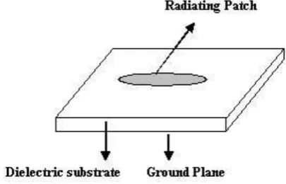
Microstrip patch antenna consists of radiating element or a metal strip on one side of the dielectric substrate and ground plane on the other side. Because the shielding ground plane is spaced a few substrate thicknesses away the dielectric substrate retains most of the power. The radiating patch may be of different shapes such as square, rectangular, thin strip, circular, elliptical, triangular or any other configuration.
Fig -1: Microstrip patch antenna
A microstrip patch antenna consists of conducting element which is a radiating patch and ground plane between them is a dielectric medium called the substrate. This substrate has particular value of dielectric constant. The dimensions of a ground plane is larger than the radiating patch. Dimensions of a microstrip patch antenna i.e. radiating patch as well as ground plane depends on the resonant frequency and value of the dielectric constant.
3.1 Different Shapes of Microstrip Patch Antenna
[image:2.595.330.533.408.538.2]© 2017, IRJET | Impact Factor value: 5.181 | ISO 9001:2008 Certified Journal | Page 1101
Fig -2: Different Shapes of Microstrip Patch antennaThe conducting patch is selected to be very thin such that t << λo (where t is the patch thickness). The height (h) of the dielectric substrate is usually 0.003 λo ≤ h ≤ 0.05 λo . The dielectric constant of the substrate (εr) is typically in the range 2.2≤ εr≤12.
4. FEEDING TECHNIQUE
To make antenna structure so that it can operate at full power of transmission feeding technique is most important in designing the antenna. Designing the feeding techniques is a difficult process for high frequency [7]. This is because the input loss of feeding increases depending on frequency and finally give huge effect on overall design. Few feeding techniques that can be used to design MPA are:
Microstip line feeding Coaxial probe feeding Aperture coupled feeding Proximity coupled feeding CPW feeding
5. THE STACKED PATCH ANTENNA
The stacked antenna is built like a multilayer printed circuit board by vertically stacking two patches i.e. one conducting patch is placed on top of the other. It is also called as multilayer antenna or dual patch antenna. The top patch is referred as radiating patch and bottom patch is referred to as feeding patch. The radiating patch is fed or excited via an electromagnetic coupling from the feeding patch [4].
Fig -3: Stacked Microstrip Patch antenna
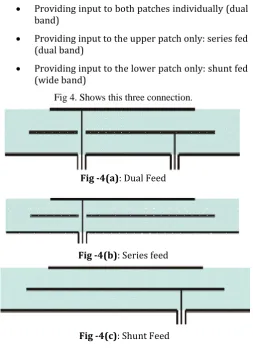
There are three ways to connect to stacked antenna as given below:
Providing input to both patches individually (dual band)
Providing input to the upper patch only: series fed (dual band)
[image:3.595.47.289.81.214.2] Providing input to the lower patch only: shunt fed (wide band)
Fig 4. Shows this three connection.
Fig -4(a): Dual Feed
Fig -4(b): Series feed
Fig -4(c): Shunt Feed
5. ANTENNA DESIGN
The design parameters of the proposed antennas are given below-
Stacked Antenna with Microstip line feed:
Ground : L=36 mm, W=34 mm Lower substrate : (Taconic, Dk = 3.0)
L = 36 mm, W = 34 mm, H (Height) = 0.8 mm Upper substrate:(FR4, Dk = 4.4)
L=36 mm, W=34 mm, H=0.5 mm Feeding patch : L=15 mm, W=13.3 mm Radiating patch : L=21.5 mm, W=18.4 mm Distance between adjacent Patches:
[image:3.595.310.564.127.477.2] [image:3.595.40.281.644.735.2]© 2017, IRJET | Impact Factor value: 5.181 | ISO 9001:2008 Certified Journal | Page 1102
Fig -5: Sixteen element stacked patch antenna6. RESULTS AND DISCUSSION
The performance of proposed antenna has been observed in terms of the return loss, VSWR and radiation pattern. By using the method of design of variables, the optimization is gained.
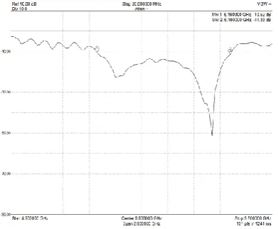
6.1 Return Loss and Bandwidth
Figure 6. Illustrates the return loss plot of the stacked antenna with microstrip line feed. The return loss and bandwidth have been increased by this technique of stacking.
Fig -6: Illustrates the return loss
[image:4.595.41.277.68.361.2]6.2 Sub Heading 2
Figure 7. VSWR of stacked microstrip patch antenna.
Fig -7: VSWR of the stacked microstrip patch antenna
The antenna is developed for the determined specification and tested using Sound Hound network analyser. The developed antenna is shown in the figure 8.
Fig -7: Perspective view of developed antenna
7. CONCLUSIONS
The proposed antenna of 16-element stacked patch is designed for 5.5 GHz and is simulated using IE3D software. The design and simulation of various microstrip antennas and arrays in C - Band such as single element, 2x2, 2x4 and 4x4 arrays has been carried out. The simulation has been carried out using IE3D software package. Further these antenna arrays have been fabricated and fully evaluated. The return loss of antenna is well below -10dB for frequency range greater than 5.2GHz. It is observed that the gain of this antenna array is greater than 20dB.
REFERENCES
[1] C. A. Balanis, “Microstrip Antennas” in Antenna Theory: Analysis and Design, 3rd ed., John Wiley & Sons, 2005, pp. 811-819.
[image:4.595.321.543.143.312.2] [image:4.595.319.549.391.482.2] [image:4.595.65.261.569.730.2]© 2017, IRJET | Impact Factor value: 5.181 | ISO 9001:2008 Certified Journal | Page 1103
Puthanial. M, International journal of science research,Issue 6, vol-3, 2014.
[3] “Design and development of Microstrip rectangular patch antenna with different feed techniques at 4 GHz”, Deepika J, A.M.Prasanna Kumar and Mohan Prasad P.
[4] B.B.Tigadi, Namita Gokavi and V.R.Udupi. “Design and Development of Microstrip Patch antenna array with Improved Performance”, IJSRd Vol 3, Issue 06, 2015.
[5] “Bandwidth Enhancement and modification of single band patch antenna into double band”, Ranjeet Pratap Singh Bhadoriya and sumit Nigam, 978-3805-4421-2/16 2016
[6] “Dual-Frequency and Polarization Antenna Array for Satellite Deployment”, Ramila Shreshtha, Dimitris E. Anagnoston, Stephen J.Horst and James P.Hoffman, 978-4673-7676-1 2016.