© 2017, IRJET | Impact Factor value: 5.181 | ISO 9001:2008 Certified Journal | Page 54
A Parallel Input Series Output DC/DC Converter with High Voltage Gain
Ajmal M M
1, Benny Cherian
2, Babu Thomas
31
PG Scholar, Dept. of EEE, Mar Athanasius College of Engineering, Kothamangalam, Kerala, India,
2Professor, Dept. of EEE, Mar Athanasius College of Engineering, Kothamangalam, Kerala, India
3Assistant Professor, Dept. of EEE, Mar Athanasius College of Engineering, Kothamangalam, Kerala, India
---***---Abstract -
The importance of high voltage gain dc/dc converter is increasing day by day. Conventional boost converter is unable to provide high gain without extreme duty ratio. An input parallel output series boost converter can provide a high step up gain. The converter uses two switches, two coupled inductors and a voltage multiplier module. The primary windings of coupled inductors are placed across the supply. Their connection reduces the input current ripple as it is shared by windings. The converter has high voltage gain and low voltage stress across power switches. The switches are turned on at zero current due to the leakage inductance of coupled inductor .The simulation of the converter is done in MATLAB/SIMULINK and results are obtained.Key Words: High step up gain, DC/DC converter, Low
voltage stress, Coupled inductors.
1. INTRODUCTION
High gain dc/dc converters are widely used in many industrial applications such as solar, fuel cell, x-rays, laser and high intensity discharge lamp ballasts for automobile headlamps[2]-[4]. Theoretically, a basic boost converter is capable of providing high conversion ratio, but extremely high duty ratio is required. In practice, extreme duty ratios are not permitted because of the large conduction losses and frequent damage of power switches. Usually it is preferable to use low voltage rated power switches having low on state resistance to reduce the conduction losses, which may not be possible in a conventional boost converter. Cascaded boost converters can provide high voltage gain[5]-[6]. But high voltage stress across the switches and poor efficiency are the disadvantages. DC/DC converters using coupled inductors is a good alternative to obtain a high step up gain[7], provided the leakage inductances are handled properly. Interleaved control is found very useful in reducing the input current ripple of the converter[8]-[10]. Two different boost converter structures can be combined to produce twice the voltage gain by connecting there inputs in parallel and output in series. The two independent inductors of this combined converter is replaced by two coupled inductors. Connecting the primary windings of coupled inductors in parallel and secondary windings in series a high step up DC/DC converter is derived. An input parallel output series boost converter with dual coupled inductors can be
used for high step up and high power applications. The interleaved control adopted reduces the input current ripple considerably. This configuration inherits the merits of high voltage gain, low voltage stress across the power switches and low output voltage ripple. Also, the converter is capable to turn on the active switches at zero current and hence reduce switching losses.
2. PARALLEL INPUT SERIES OUTPUT DC/DC
CONVERTER
2.1 Input parallel output series boost converter
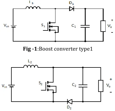
The input parallel output series concept is explained in Fig -1 to 3. The basic boost converter topology is shown in Fig -1 and Fig -2 is another boost version with the same function in which the output diode is placed on the negative dc rail. Fig -3 is called a modified interleaved boost converter, which is an input-parallel and output-series configuration derived from two basic boost types. The derived converter has twice the voltage gain of a conventional boost converter, low output voltage ripple and low input current ripple due to interleaved control.
Fig -1:Boost converter type1
[image:1.595.332.534.500.695.2]© 2017, IRJET | Impact Factor value: 5.181 | ISO 9001:2008 Certified Journal | Page 55
Fig -3: Parallel input series output DC/DC Converter
The separate inductors of Fig - 3 are modified by coupled inductors whose primary windings are connected in parallel and secondary windings in series as shown in Fig - 4. A voltage multiplier module is connected in the output to get a higher voltage gain. This connection has several advantages compared to conventional interleaved boost converter.
Fig -4: Input parallel output series DC/DC converter with high voltage gain
2.2 Operation of the converter
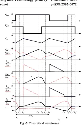
The converter is operated in continuous conduction mode(CCM). 1800 interleaved overlapped pulses (Duty ratio greater than 50%) are used for the power switches. There are three switching states as S1 : ON, S2 : ON; S1 : ON, S2 : OFF; S1: OFF, S2 : ON. Operation of the converter can be explained through eight modes in the above mentioned control scheme. The basic working principle is as explained below. The theoretical waveforms of the converter are shown in Fig -5. The schematic diagram in each operating mode is shown in Fig -6 to Fig -13.
Fig -5: Theoretical waveforms
Mode 1[t0-t1]:- At t=t0 Switch S1 is turned on at zero current switching due to the leakage inductance of LK1 . S2 remains turned on from the previous state as shown in Fig -6. All diodes except output diode D3 is turned off. This phase ends when the current through D3 decreases to zero.
Fig -6: Mode 1
[image:2.595.304.571.57.468.2] [image:2.595.46.283.91.239.2] [image:2.595.45.281.349.544.2] [image:2.595.316.552.554.742.2]© 2017, IRJET | Impact Factor value: 5.181 | ISO 9001:2008 Certified Journal | Page 56 reversed-biased. The voltage source Vin charges
magnetizing inductances Lm1 and Lm2 as well as leakage inductances Lk1 and Lk2. This stage ends at t2, when S2 is turned off.
Fig -7: Mode 2
Mode 3[t2-t3]:- The switch S2 is turned off at t = t2, hence the diodes D2 and Dr turned on. The current flow direction is shown in Fig -8. The energy that has stored in magnetizing inductance Lm2 is transferred to the secondary side, charging the capacitor Cr through Dr. The input voltage source Vin, magnetizing inductance Lm2 and leakage inductance Lk2 deliver energy to the capacitor C2 through diode D2.
Fig -8: Mode3
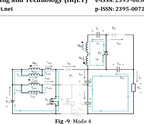
Mode 4[t3-t4]:- when the total energy of leakage inductance Lk2 has been completely delivered to the capacitor C2 at t = t3, diode D2 automatically switches off. The current flow path of this stage is shown in Fig -8. Magnetizing inductance Lm2 will transfer energy to the secondary side charging the capacitor Cr through diode Dr. The sum of currents of the magnetizing inductances Lm1 and Lm2 flows throughthe switch S1.
Fig -9: Mode 4
[image:3.595.308.555.56.269.2]Mode 5[t4-t5]:- The switch S1 remains turned on at t = t4, the switch S2 is turned on with ZCS due to the leakage inductance Lk2. The current flow direction of this stage is shown in Fig -10. This stage ends when the current through the diode Dr reduces to zero at t =t5.
Fig -10: Mode 5
Mode 6[t5-t6]:- Operating modes 2 and 6 are same. All diodes are turned off. The magnetizing inductances Lm1, Lm2, and the leakage inductances Lk1, Lk2 are charged by the source.
Fig -11: Mode 6
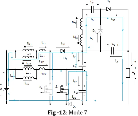
[image:3.595.44.281.149.324.2] [image:3.595.315.551.333.502.2] [image:3.595.44.281.425.597.2] [image:3.595.316.551.553.749.2]© 2017, IRJET | Impact Factor value: 5.181 | ISO 9001:2008 Certified Journal | Page 57 conduction. The current flow path of this stage is shown in
[image:4.595.46.282.173.370.2]Fig -12. The source Vin, Lm1 and Lk1 together release their energy to the capacitor C1 through the switch S2. At the same time, the energy stored in Lm1 is released to the secondary side. D3 is conducting and the current through the secondary sides will flow to load and capacitor C3.
Fig -12: Mode 7
[image:4.595.46.280.456.651.2]Mode 8[t7-t8]:- At time t = t7, diode D1 gets turned off because the total energy of leakage inductance Lk1 has been completely transferred to the capacitor C1. The current of the magnetizing inductance Lm1 continues to flow to the output through the secondary side of coupled inductor and D4 until t0.
Fig -13: Mode 8
3. CIRCUIT ANALYSIS AND DESIGN
3.1 Voltage gain expression
Take two identical coupled inductors. Using the volt-second balance principle on magnetizing inductances Lm1 and Lm2 respectively, the voltage gain (mCCM) can be obtained as, [1]
(1)
Where k is the leakage factor of coupled inductors, N is the turns ratio and D is the duty ratio.3.2 Voltage stress analysis
To simplify the voltage stress analyses of the components, the leakage inductance of coupled inductor and the voltage ripples on the capacitors are ignored. The voltage stresses on power switches S1 and S2 for an output voltage V0 are derived as, [1]
(2)
3.3 Coupled inductor design
From the voltage gain equation, the turns ratio of coupled inductor can be designed as, [1]
(3)
3.4 Capacitor design
The filter capacitors are designed considering the voltage ripple(ΔVC) across it, for switching frequency fs and load resistance R the capacitor values are estimated according to below equations [1]
(4)
(5)
(6)
(7)
2. SIMULATION AND RESULTS
© 2017, IRJET | Impact Factor value: 5.181 | ISO 9001:2008 Certified Journal | Page 58
Fig -14: Simulink model IPOS high gain converter
[image:5.595.116.533.255.732.2]Fig -15: Control pulses of switches
Table -1: Simulation parameters.
Parameter
Value
Po 100W
Vin 20
Magnetizing inductance, Lm1,Lm2
242 µ H
Capacitors C1, C2 47 µ F
Capacitor C3 100 µ F
Capacitor Cr 10 µ F
Switching frequency, fs 40kHz
Vout 200
Fig - 16, 17 respectively shows the voltage across and current flowing through the switches 1 and 2. The voltage stress across the switch is a quarter of the output and switches are turned on at zero current.
[image:5.595.327.540.258.733.2]Fig -16: Soft switching of switch S1
Fig -17: Soft switching of switch S2
It is clear from the waveforms that the switches are turned on with zero current turn on due to the leakage inductance present in the path and hence switching losses are reduced.
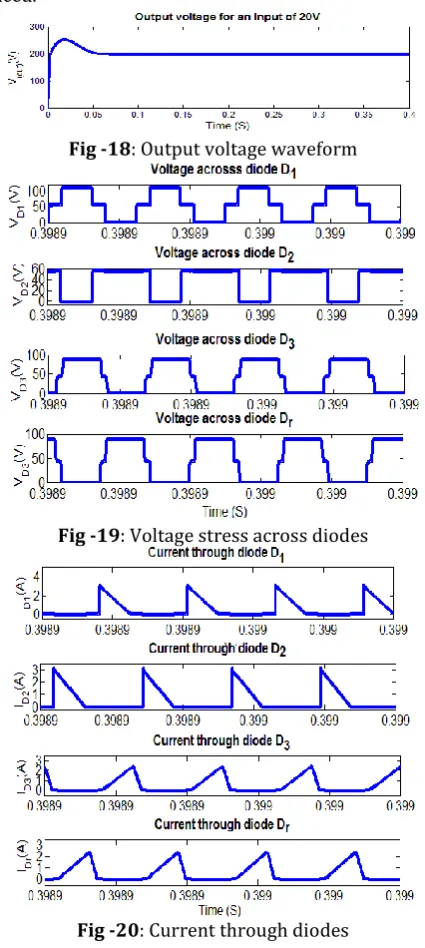
Fig -18: Output voltage waveform
Fig -19: Voltage stress across diodes
© 2017, IRJET | Impact Factor value: 5.181 | ISO 9001:2008 Certified Journal | Page 59
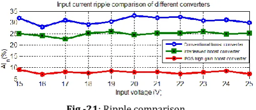
Fig -21: Ripple comparison
The output voltage with an input of 20V shown in Fig - 18 proves that the converter achieves the expected voltage gain with a low duty ratio of 0.6. Fig -19 and Fig -20 respectively show the voltage across and current flowing through the diodes. Ripple comparison shown in Fig -21 proves that the converter has a very less input current ripple compared to conventional boost/interleaved boost converter.
3. CONCLUSIONS
An parallel input series output DC/DC converter using dual coupled inductors is found to be a good candidate for low input voltage, high voltage gain applications. The converter can achieve a much higher voltage gain and avoid operating at extreme duty cycle and numerous turn's ratios. A voltage gain of 10 is obtained by operating at a duty ratio of 0.6 with turns ratio 1. The voltage stresses of the power switches are very low, which is 25% of the output voltage. Interleaved control reduces the input current ripple effectively. The output voltage ripple is calculated as 0.02%. The simulation results show that main switches can be turned on at zero current.
REFERENCES
[1] Xuefeng Hu, Chunying Gong, “A high gain input-parallel output-series dc/dc converter with dual coupled inductors” IEEE Transactions on Power Electron., vol. 30, no. 3, pp. 1306–1317, March. 2015. [2] Florent Boico, Brad Lehman, and Khalil Shujaee,
“Solar battery chargers for NiMH batteries,” IEEE Transactions on Power Electron., vol. 22, no. 5, pp. 1600–1609, Sep. 2007.
[3] Z. Amjadi and S. S. Williamson,“Power-electronics-based solutions for plug-in hybrid electric vehicle energy storage and management systems,”IEEE Trans. Ind. Electron., vol. 57, no. 2, pp. 608–616, Feb.2010. [4] G. Fontes, C. Turpin, S. Astier, and T. A. Meynard,
“Interactions between fuel cell and power converters: Influence of current harmonics on a fuel cell stack,”IEEE Trans. Power Electron., vol. 22, no. 2, pp. 670–678, Mar. 2007.
[5] S. Chen, T. Liang, L. Yang, and J. Chen, “A cascaded high step-up dc–dc converter with single switch for microsource applications,” IEEE Trans. Power Electron., vol. 26, no. 4, pp. 1146–1153, Apr. 2011 [6] S.V, J-P F, and Y. L, “Optimization and design of a
cascaded DC/DC converter devoted to grid connected
Photovoltaic systems,” IEEE Trans.Power Electron., vol. 27, no. 4, pp. 2018–2027, Apr. 2012.
[7] S.V, J-P F, and Y. L, “Optimization and design of a cascaded DC/DC converter devoted to grid connected Photovoltaic systems,” IEEE Trans.Power Electron., vol. 27, no. 4, pp. 2018–2027, Apr. 2012.
[8] W. Li, Y. Zhao, J.Wu and X. He, `Interleaved high step-up converter with winding-cross-costep-upled inductors and voltage multiplier cells", IEEE Transactions on Power Electronics, vol. 27, no. 1, pp. 133143, Jan. 2012 [9] G A. L. Henn, R. N. A. L. Silva, P P. Praca, L H. S. C.
Barreto, and D S.Oa, Jr. Interleaved-boost converter with high voltage gain", IEEE Transactions on Power Electronics, vol. 25, no. 11,pp. 27532761, Nov. 2010. [10] C. M. Lai, C. T. Pan, and M. C. Cheng High effciency
modular high step up interleaved boost converter for DC microgrid applications" IEEE Transactions Industrial Applications, vol. 48, no. 1, pp. 161171, Jan/Feb, 2012.