http://dx.doi.org/10.4236/opj.2016.67020
All-Optical 3:8 Decoder with the Help of
Terahertz Optical Asymmetric
Demultiplexer
Dilip Kumar GayenDepartment of Computer Science & Engineering, College of Engineering & Management, Kolaghat, KTPP Township, Purba Medinipur, India
Received 26 May 2016; accepted 25 July 2016; published 28 July 2016
Copyright © 2016 by author and Scientific Research Publishing Inc.
This work is licensed under the Creative Commons Attribution International License (CC BY).
http://creativecommons.org/licenses/by/4.0/
Abstract
An all-optical 3:8 decoder unit with the help of terahertz optical asymmetric demultiplexer (TOAD) is proposed. The all-optical 3:8 decoder unit with a set of all-optical full-adders and optical exclu-sive-ORs (XORs), can be used to perform a fast central processor unit using optical hardware components. We try to exploit the advantages of TOAD-based optical switch to design an inte-grated all-optical circuit which can perform decoding of signal. A theoretical model is presented and verified through numerical simulation. The new method promises both higher processing speed and accuracy. The model can be extended for studying more complex all-optical circuit of enhanced functionality in which decoder is the basic building block. The operation of the pro-posed circuit is parallel in nature. The impact of the switching energy with small signal gain and variation of extinction ratio and contrast ration with control pulse energy of the switching out-come is explored and assessed by means of numerical simulations.
Keywords
Terahertz Optical Asymmetric Demultiplexer, Semiconductor Optical Amplifier, Optical Logic
1. Introduction
communication systems and optical computing. Various architectures, algorithms, logical, and arithmetic opera-tions have been proposed in the field of optical-optoelectronic computing and parallel signal processing in the past few decades [1]-[7]. A revolution has been brought about in all-optical information processing system with the help of the discovery of ultra high speed all-optical switches based on cross phase modulation. Among dif-ferent optical switches, the terahertz optical asymmetric demultiplexer (TOAD) gate effectively combines fast switching time, high repetition rate, and low power consumption [8]-[10]. An all-optical half-adder using SOA-assisted Sagnac interferometer has been suggested and demonstrated by several groups of researches [1] [11]-[15]. Ghosh et al. have reported a new method of implementing all-optical frequency encoded logic opera-tions and half-adder by the use of SOA as well as Mach-Zehnder interferometer [16]. A novel scheme for an ultra- high speed all-optical half-adder based on four waves mixing in semiconductor optical amplifiers has been demonstrated by Li [17]. Kim et al. have demonstrated how all-optical full-adder utilizes the mechanism of cross-gain modulation [18]. All-optical full-adder with bit differential delay has been reported by Poustie [19]. A complete analytical model of all-optical half-adder and full-adder has been proposed based on the principle of phase encoding technique [20]. Ghosh et al. have proposed a new scheme of implementing a wavelength en-coded complete binary full-adder and full-subtractor unit in all-optical domain using the wavelength conversion by the nonlinear polarization rotation in a single semiconductor optical amplifier [21]. A novel frequency en-coded all-optical half-adder, half-subtractor, and full-adder have been suggested by Mukherjee [22]. J. Wang et al. have proposed all-optical simultaneous half-adder, half-subtractor, and OR logic gate at 40 Gbit/s based on the cascaded sum and difference-frequency generation using periodically poled lithium niobate waveguide [23]. Cascading of two TOAD based switches has been demonstrated by B. C. Wang [7]. A terahertz-optical-asymmetric demultiplexer (TOAD)-based gate has already taken a significant role in the field of ultrafast all-optical infor-mation processing.
In this paper, we have tried to take the output from both the transmitting and reflecting mode of the device. That is, light coming out from both the input and the output ports is taken into account. With the help of TOAD-based switches, we propose decoder unit that can work in all-optical domains. The proposed all-optical schemes can exhibit its switching speed far above present-day electronic circuits. The operation of the proposed circuit is parallel in nature.
2. Operation of TOAD Based Switch
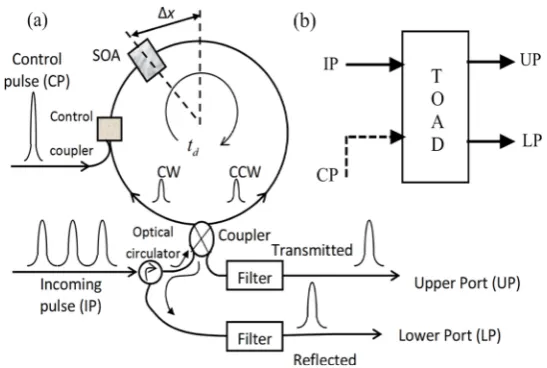
The basic design of TOAD based switch is shown in Figure 1(a)[8][24]. Here a nonlinear element (NLE) is placed asymmetrically in a loop. The coon NLE is semiconductor optical amplifier (SOA). In this paper, we have tried to use the output from both the transmitting and reflecting mode of the device. The output power at upper and lower can be expressed as [8][25]
( )
( )
{
( )
( )
2( )
( )
cos( )
}
4
in
UPPER cw ccw cw ccw
P t
P t = ⋅ G t +G t − G t ⋅G t ⋅ ∆ϕ (1)
( )
( )
{
( )
( )
2( )
( )
cos( )
}
4
in
LOWER cw ccw cw ccw
P t
P t = ⋅ G t +G t + G t ⋅G t ⋅ ∆ϕ (2)
where, Gcw
( )
t G, ccw( )
t is the power gain. The time-dependent phase difference between clockwise (CW) and counter clockwise (CCW) pulses [25] is ∆ = −ϕ α 2. ln(
Gcw( )
t Gccw( )
t)
with α being the line-widthen-hancement factor. In the absence of a control signal, data signal (incoming signal) enters the fiber loop, pass through the SOA at different times as they counter-propagate around the loop, and experience the same unsatu-rated small amplifier gain Gss, and recombine at the input coupler i.e.Gccw ≈ Gcw. Then, ∆ ≈ϕ 0 and expression for PUpper
( )
t ≈0 and PLower( )
t =Pin( )
t ⋅Gss. It shows that data is reflected back toward the source. When a control pulse is injected into the loop (CP=on), it saturates the SOA at time ts and changes its index of refrac-tion. The gain of the SOA decreases rapidly as [25][26]:( )
( )
0
1
1
1 1 exp cp
sat G t
E t
G E
=
− − −
(3)
Figure 1. (a) A TOAD based optical switch with single control pulse (CP), where SOA: Semiconductor optical amplifier, CW: Clockwise pulse, CCW: Counterclockwise pulse and Δx: asymmetric distance. (b) The schematic diagram of TOAD based switch.
( )
( )
dt
cp cp
E t P t t
−∞
′ ′
=
∫
is the energy fraction contained in the leading edge of the pulse until the moment t′ ≤t.By definition Ecp
(
t→ ∞ =)
Ec = total energy of the control pulse. Here we consider Gaussian pulse( )
πexp 22cp cp E t P t σ σ = −
as control signal. Ecp is the control pulse energy. σ is related to full width at half maximum (FWHM) by TFWHM ≅1.665σ. Then we can write
( )
12
c cp
E t
E t erf
σ
= +
(4) where erf(.) is the error function. The SOA saturation time ts ≈TFWHM, then 99% of the pulse transmits through SOA. As a while the gain recovers due to injection of carriers and can be obtained from the gain recovery for-mula [25][26],
( )
( )
( ) exp 0 0 ; s e t t s s G tG t G t t
G τ − − = ≥
(5)
where, τe is the gain recovery time. When periodic pulse train inserted in the SOA, then there is no time to recovery of the gain to G0, but to a lower one Gl [25][26]. Hence Equation (3) takes the form,
( )
{
(
)
( )
}
11 1 1 l exp cp sat
G t = − − G −E t E − (6)
Now, from the above equation we find,
( )
(
)
(
)
1 exp
l
f s
l l c sat
G
G G t
G G E E
= =
− − − (7)
Now at next bit period (ξ), SOA gain does not reach to G0 but Gl. So,
( )
{ ( ) } exp 0 0 FWHM e T f l GG G G
G ξ τ ξ − − = =
(8)
( ) ( )
{exp exp }
0
s e s e
t T t t t
f ccw
cw G G
G G
τ τ
− + − − − −
=
(9)
where T is the eccentricity of the loop. Therefore when they recombine at the input coupler, then ∆ ≈ −ϕ π and the data will exit from the upper port i.e. PUpper
( )
t ≠0 and PLower( )
t ≈0, the corresponding values can beob-tained from the Equations ((1) and (2)), respectively. The energy of the control pulse is ten times greater than that of the incoming pulse. A filter may be used at the output of TOAD based switch to reject the control and pass the incoming pulse. The schematic diagram of TOAD based switch is shown in Figure 1(b).
3. All-Optical 3:8 Decoder
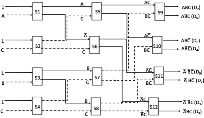
A decoder is a combinational circuit that converts binary information from n input lines to a maximum of 2n unique output lines. The only inputs in decoders are the control bits. In digital electronics, a decoder can take the form of a multiple-input, multiple-output logic circuit that converts coded inputs into coded outputs, where the input and output codes are different e.g. n to 2n. A block diagram of 3:8 decoder (3 input lines and 8 output lines) is shown in Figure 2. To implement the optical 3:8 decoder, we use TOAD-based optical switches, namely s1 to
s12 as shown in Figure 2 which has three select inputs (A, B and C). It is to be noted that the output of a
TOAD-based switch can be used as a control signal for the other provided its intensity is increased suitably through an erbium-doped fiber amplifier and the wavelength is changed through a wavelength converter. The solid lines indicate that the output of one switch is directly connected to input of another switch. The dotted lines indicate that the output of one switch is connected to input of another via wavelength converted and er-bium-doped fiber amplifier.
When 1 i.e. presence of incoming signal and A is incident on s1, light emerging through the upper channel is
A and light emerging through lower channel is A̅. Similarly, when 1 and C is incident on s2, light emerging
through the upper channel is C and light emerging through lower channel is C̅. Again when 1 and B are incident on s3, light emerging through the upper channel is B and light emerging through lower channel is B̅. Finally
when 1 and C are incident on s4 light emerging through the upper channel is C and light emerging through lower
channel is C̅.
Again, When A and C are incident on s5, light emerging through the upper channel is AC and light emerging
through lower channel is AC̅. Similarly when A̅ and C̅ are incident on s6, light emerging through the upper
channel is A̅C̅ and light emerging through lower channel is A̅C. Again when B and C are incident on s7 light
emerging through the upper channel is BC and light emerging through lower channel is BC̅. Finally when B̅ and C̅ are incident on s8 light emerging through the upper channel is B̅C̅ and light emerging through lower channel is
[image:4.595.134.492.501.708.2]B̅C. The eight cases are described in detail.
Case 1: When AC and BC are fed into s9, light emerging through the upper channel is ABC.
Case 2: When AC and BC are fed into s9, light emerging through the lower channel is AC(B̅+C̅)=AB̅C. Case 3: When AC̅ and BC̅ are fed into s10, light emerging through the upper channel is ABC̅.
Case 4: When AC̅ and BC̅ are fed into s10, light emerging through the upper channel is AC̅(B̅+C)=AB̅C̅. Case 5: When A̅C̅ and B̅C̅ are fed into s11, light emerging through the upper channel is A̅B̅C̅.
Case 6: When A̅C̅ and B̅C̅ are fed into s11, light emerging through the upper channel is A̅BC̅. Case 7: When A̅C and B̅C are fed into s12, light emerging through the upper channel is A̅B̅C. Case 8: When A̅C and B̅C are fed into s12, light emerging through the upper channel is A̅BC.
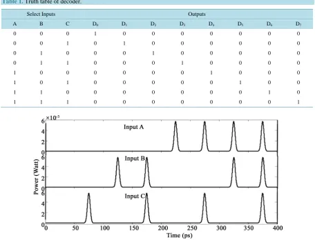
The above observations are put in a table as shown in Table 1. This verifies the operation of 3:8 decoder.
4. Simulated Results
The parameters used in this simulation are taken from the literature survey of different research papers [1][2] [25][26]. The values of different parameters as : unsaturated amplifier gain of the SOA (Gss) = 30 dB, gain re-covery time of SOA (τe) = 90 ps, saturation energy of the SOA (Esat) = 1000 fJ, eccentricity of the loop (Tasym) = 30 ps, line-width enhancement factor (α) = 6, full width at half maximum of control pulse (σ) = 6 ps, bit period (Tc) = 100 ps, and a control pulse energy (Ecp) = 100 fJ so that the operational conditions are satisfied. The si-mulated input waveforms are shown in Figure 3. The simulated output waveforms are shown in Figure 4.
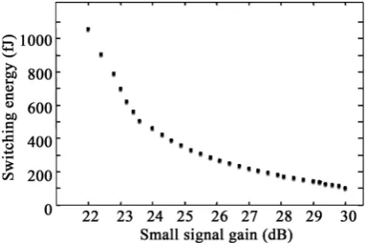
[image:5.595.84.541.358.706.2]To study the operation of the circuit, we find the appropriate value of the SOA small signal gain for which switching energy is minimized. For this reason, the switching energy’s dependence on the small signal gain is plotted in Figure 5. It can be seen from this figure that the energy decreases exponentially with the increase of small signal gain and reaches a minimum value of 100 fJ at 20 dB.
Table 1. Truth table of decoder.
Select Inputs Outputs
A B C D0 D1 D2 D3 D4 D5 D6 D7
0 0 0 1 0 0 0 0 0 0 0
0 0 1 0 1 0 0 0 0 0 0
0 1 0 0 0 1 0 0 0 0 0
0 1 1 0 0 0 1 0 0 0 0
1 0 0 0 0 0 0 1 0 0 0
1 0 1 0 0 0 0 0 1 0 0
1 1 0 0 0 0 0 0 0 1 0
1 1 1 0 0 0 0 0 0 0 1
Figure 4.Simulated output waveforms, where power (Watt) is along the y-axis whereas time (ps) is along the x-axis.
Figure 5. Variation of switching energy versus small signal gain.
This is an expected behavior of the switch, since higher small signal gain values drastically affect the SOA dynamics and can induce larger differential gain between the counter-propagating clock components, so that switching can be achieved with less energy. Inversely, a larger energy is required to compensate for the decrease of small signal gain and deeply saturate the SOA, so that the necessary gain changed is occurred.
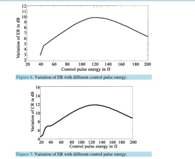
In order to assess the performance of the circuit at 20 Gbit/s, we define different suitable metrics for this pur-pose. The most suitable metrics are the extinction ratio and contrast ratio. The extinction ratio (ER) is define as
( )
min10 max
ER dB 10 log P
P
=
, (10) where Pmin1 and
0 max
P is the minimum and maximum peak power of the 1-states and 0-states, respectively, and the contrast ratio (CR) is
( )
mean10 mean
CR dB 10 log P
P
=
, (11) where Pmean1 and
0 mean
[image:6.595.210.421.275.416.2]Figure 6. Variation of ER with different control pulse energy.
Figure 7. Variation of ER with different control pulse energy.
pulse energy is reduced from some specified value then it cannot alter significantly the SOA properties, that is insufficient to create the necessary differential shift and hence reduces the matrices variation.
On the other hand, if the control pulse energy is increased from some specified value (~100 fJ) then the SOA becomes strongly saturated so that the counter clock-wise pulse has enough time to see a partly recovered gain, that is also insufficient to create the necessary differential shift and hence reduces the matrices variation.
From Figures 5-7 and their explanation, it can be inferred that the requirements for the critical parameters are
Gss = 20 dB, τe = 100 ps, Ecp = 100 fJ, Esat = 1000 fJ, Tasym = 30 ps, α = 6, σ = 12 ps, and ξ = 50 ps respectively, which obviously is not unique and falls within the specified boundaries. Then by combining these values with those held constant throughout the simulation, we can obtain ER = 8.71 dB and CR = 11.67 dB at outputs re-spectively of the circuit configuration. Therefore all considered performance metrics are more that acceptable, which is reflected on the quality of the pulse stream obtained at the outputs [28]. The eye-diagram [29] is the superposition of the outputs for the repetition period of the inputs. The high quality of the obtained pseudo-eye diagram (PED) is further supported by its relative eye opening (O) defined as O=
(
Pmin1 −Pmax0)
Pmin1 ,1 min
P
and Pmax0 are the minimum and maximum powers at 1-state and 0-state, respectively. An eye-diagram with
large eyes indicates a clear transmission with a low bit error rate. Here, we get PED (O) = 82.88% at the outputs, respectively, which indicates an excellent response of the circuit to the incoming data at its output terminals.
5. Conclusion
all-optical circuits. The model can be extended for studying more complex all-optical circuits of enhanced func-tionality in which the proposed circuit developed in this paper may be assumed as the basic building blocks.
Acknowledgements
The authors are grateful to Technical Education Quality Improvement Programme (TEQIP) phase II by National Project Implementation Unit (Approval No.—CEMK/TEQIP-lI/R&D/Project/15-16/03) for providing the grant for this work.
References
[1] Zoiros, K.E., Vardakas, J., Houbavlis, T. and Moyssidis, M. (2005) Investigation of SOA-Assisted Sagnac Recirculat-ing Shift Register SwitchRecirculat-ing Characteristics. International Journal for Light and Electron Optics, 116, 527-541.
http://dx.doi.org/10.1016/j.ijleo.2005.03.005
[2] Bhattacharyya, A., Gayen, D.K. and Chattopadhyay, T. (2013)All-Optical Binary Coded Decimal to Binary Converter with the Help of Terahertz Asymmetric Demultiplexer Based Switch. Proceedings of 5th International Conference on
Computers and Devices for Communication (CODE), Kolkata, 17-19 December 2012, 1-4.
http://dx.doi.org/10.1109/CODEC.2012.6509307
[3] Suzuki, M. and Uenohara, H. (2009) Invesigation of All-Optical Error Detection Circuitusing SOA-MZI Based XOR Gates at 10 Gbit/s. Electronics Letters, 45, 224. http://dx.doi.org/10.1049/el:20093461
[4] Minh, H.L., Ghassemlooy, Z. and Ng, W.P. (2008) Characterization and Performance Analysis of a TOAD Switch Employing a Dual Control Pulse Scheme in High Speed OTDM Demultiplexer. IEEE Communications Letters, 12, 316-318. http://dx.doi.org/10.1109/LCOMM.2008.061299
[5] Li, G. (2009) Recent Advances in Coherent Optical Communication. Advances in Optics and Photonics, 1, 279-307.
http://dx.doi.org/10.1364/AOP.1.000279
[6] Bhattacharyya, A., Gayen, D.K. and Chattopadhyay, T. (2012) 4-Bit All-Optical Binary to Two’s Complement Con-verter. Proceedings of International Conference on Communications, Devices and Intelligent Systems, Kolkata,28-29 December 2012, 496-499. http://dx.doi.org/10.1109/codis.2012.6422247
[7] Wang, B., Baby, V., Tong, W., Xu, L., Friedman, M., Runser, R., Glesk, I. and Prucnal, P. (2002) A Novel Fast Opti-cal Switch Based on Two Cascaded Terahertz OptiOpti-cal Asymmetric Demultiplexers (TOAD). Optics Express, 10, 15-23.
http://dx.doi.org/10.1364/OE.10.000015
[8] Sokoloff, J.P., Prucnal, P.R., Glesk, I. and Kane, M. (1993) A Terahertz Optical Asymmetric Demultiplexer (TOAD).
IEEE Photonics Technology Letters, 5, 787-790. http://dx.doi.org/10.1109/68.229807
[9] Wang, H., Wu, J. and Lin, J. (2005) Performance Analysis on Terahertz Optical Asymmetric Demultiplexer with As-sist Light Injection. Optics Communications, 256, 83-97. http://dx.doi.org/10.1016/j.optcom.2005.06.037
[10] Parolari, P., Boffi, P., Marazzi, L. and Martinelli, M. (2003) Two-Stage Sagnac Demultiplexer. Journal of Lightwave
Technology, 21, 1808-1812. http://dx.doi.org/10.1109/JLT.2003.815508
[11] Poustie, A.J., Blow, K.J., Kelly, A.E. and Manning, R.J. (1998) All-Optical Binary Half-Adder. Optics
Communica-tions, 156, 22-26. http://dx.doi.org/10.1016/S0030-4018(98)00349-6
[12] Kim, S.H., Kim, J.H., Choi, J.W., Son, C.W., Byun, Y.T., Jhon, Y.M., Lee, S., Woo, D.H. and Kim, S.H. (2006) All- Optical Half-Adder Using Cross-Gain Modulation in Semiconductor Optical Amplifiers. Optics Express, 14, 10693- 10698. http://dx.doi.org/10.1364/OE.14.010693
[13] Gayen, D.K., Chattopadhyay, T., Bhattacharyya, A., Basak, S. and Dey, D. (2014) All-Optical Half Adder/Subtractor Using Terahertz Optical Asymmetric Demultiplexer. Applied Optics, 53, 8400-8409.
[14] Kim, J.H., Byun, Y.T., Jhon, Y.M., Lee, S., Woo, D.H. and Kim, S.H. (2003) All-Optical Half-Adder Using Semicon-ductor Optical Amplifier Based Devices. Optics Communications, 218, 345-349.
http://dx.doi.org/10.1016/S0030-4018(03)01203-3
[15] Chen, Z. (2010) Simple Novel All-Optical Half-Adder. Optical Engineering, 49, 43201-43206.
http://dx.doi.org/10.1117/1.3366669
[16] Ghosh, B., Pal, R.R. and Mukhopadhyay, S. (2011) A New Approach to All-Optical Half-Adder by Utilizing Semi-conductor Optical Amplifier Based MZI Wavelength Converter. Optik—International Journal for Light and Electron
Optics, 122, 1804-1807. http://dx.doi.org/10.1016/j.ijleo.2010.10.042
[17] Li, P., Huang, D., Zhang, X. and Zhu, G. (2006) Ultra-High Speed All-Optical Half-Adder Based on Four Wave Mix-ing in Semiconductor Optical Amplifier. Optics Express, 14, 11839-11847. http://dx.doi.org/10.1364/OE.14.011839
Kim, S.H. (2005) Realization of All-Optical Full-Adder Using Cross-Gain Modulation. Proceedings of the Conference
on Semiconductor Lasers and Applications, SPIE, 5628, 333-340. http://dx.doi.org/10.1117/12.576410
[19] Poustie, A., Blow, K.J., Kelly, A.E. and Manning, R.J. (1999) All-Optical Full-Adder with Bit Differential Delay.
Op-tics Communications, 168, 89-93. http://dx.doi.org/10.1016/S0030-4018(99)00348-X
[20] Mukhopadhyay, S. and Chakraborty, B. (2009) A Method of Developing Optical Half- and Full-Adders Using Optical Phase Encoding Technique. Proceedings of the Conference on Communications, Photonics, and Exhibition (ACP), Shanghai, 2-6 November 2009, 1-2.
[21] Ghosh, P., Kumbhakar, D., Mukherjee, A.K. and Mukherjee, K. (2011) An All-Optical Method of Implementing a Wavelength Encoded Simultaneous Binary Full-Adder-Full-Subtractor Unit Exploiting Nonlinear Polarization Rota-tion in Semiconductor Optical Amplifier. Optik—International Journal for Light and Electron Optics, 122, 1757-1763.
http://dx.doi.org/10.1016/j.ijleo.2010.10.039
[22] Mukherjee, K. (2011) Method of Implementation of Frequency Encoded All-Optical Half-Adder, Half-Subtractor, and Full-Adder Based on Semiconductor Optical Amplifiers and Add Drop Multiplexers. Optik—International Journal for
Light and Electron Optics, 122, 1188-1194. http://dx.doi.org/10.1016/j.ijleo.2010.07.026
[23] Wang, J., Sun, J. and Sun, Q. (2007) Single-PPLN-Based Simultaneous Half-Adder, Half-Subtracter, and OR Logic Gate: Proposal and Simulation. Optics Express, 15, 1690-1699. http://dx.doi.org/10.1364/OE.15.001690
[24] Sokoloff, J.P., Glesk, I., Prucnal, P.R. and Boneck, R.K. (1994) Performance of a 50 Gbit/s Optical Time Domain Mul-tiplexed System Using a Terahertz Optical Asymmetric Demultiplexer. IEEE Photonics Technology Letters, 6, 98-100.
http://dx.doi.org/10.1109/68.265902
[25] Eiselt, M., Pieper, W. and Weber, H.G. (1995) SLALOM: Semiconductor Laser Amplifier in a Loop Mirror. Journal of
Lightwave Technology, 13, 2099-2112. http://dx.doi.org/10.1109/50.469721
[26] Gayen, D.K., Chattopadhyay, T., Das, M.K., Roy, J.N. and Pal, R.K. (2011) All-Optical Binary to Gray Code and Gray to Binary Code Conversion Scheme with the Help of Semiconductor Optical Amplifier-Assisted Sagnac Switch. IET
Circuits, Devices & Systems, 5, 123-131. http://dx.doi.org/10.1049/iet-cds.2010.0069
[27] Houbavlis, T., Zoiros, K.E., Kanellos, G. and Tsekrekos, C. (2004) Performance Analysis of Ultrafast All-Optical Boolean XOR Gate Using Semiconductor Optical Amplifier-Based Mach-Zehnder Interferometer. Optics
Communica-tions, 232, 179-199. http://dx.doi.org/10.1016/j.optcom.2003.12.062
[28] Houbavlis, T. and Zoiros, K.E. (2003) 10-GHz All-Optical Recirculating Shift Register with Semiconductor Optical Amplifier (SOA)-Assisted Sagnac Switch and SOA Feedback. Optical Engineering, 42, 2483-2484.
http://dx.doi.org/10.1117/1.1599363
[29] Gutierrez-Castrejon, R., Occhi, L., Schares, L. and Guekos, G. (2001) Recovery Dynamics of Cross-Modulated Beam Phase in Semiconductor Amplifiers and Applications to All-Optical Signal Processing. Optics Communications, 195, 167-177. http://dx.doi.org/10.1016/S0030-4018(01)01315-3
Submit or recommend next manuscript to SCIRP and we will provide best service for you:
Accepting pre-submission inquiries through Email, Facebook, LinkedIn, Twitter, etc. A wide selection of journals (inclusive of 9 subjects, more than 200 journals) Providing 24-hour high-quality service
User-friendly online submission system Fair and swift peer-review system
Efficient typesetting and proofreading procedure
Display of the result of downloads and visits, as well as the number of cited articles Maximum dissemination of your research work
![MD5 considered harmful today [vangelis] pdf](data:image/gif;base64,R0lGODlhAQABAIAAAP///wAAACH5BAEAAAAALAAAAAABAAEAAAICRAEAOw==)