OPTIMIZATION OF INSULATED HfO2 DIELECTRICS OF GaN/InN/GaN/
In0.1Ga0.9N ENHANCEMENT MODE OF MIS-HEMT HETEROSTRUCTURE
FOR HIGH FREQUENCY POWER AMPLIFIER APPLICATIONS
Y. Tarauni
1,*, Y. Shehu
2, M. Auwal
3and A. Rakiya
41, 2, 3, 4,
D
EPARTMENT OFP
HYSICS,
K
ANOU
NIV.
OFS
CIENCE&
T
ECH.,
W
UDIL–
K
ANO,
K
ANOS
TATE,
NIGERIA.
E-mail addresses:
1[email protected],
2[email protected],
3[email protected],
4
[email protected]
ABSTRACT
In this paper, the enhancement-mode operation of the hetestructure of GaN/InN/GaN/In0.1Ga0.9N
of the Metal Insulator Semiconductor High Electron Mobility Transistor (MIS-HEMTs) device having lnN-channel was investigated. The effect of scaling the device dimensions of Metal Insulator, such
as the dielectric thickness of HfO2 and the channel lengths, on the electrical performances was
analyzed and compared to the currently used heterostructure. The numerical simulation of synopsis TCAD used showed a significant improvement in the electrical properties of the device that achieved
a threshold voltage (VT)= 0.828 maximum drain current of 1.77 A/mm V, transconductance (gm) of
2.29 S.mm−1, lowest ON-state resistance (RON) of 0.21 Ω.mm, and along with high-frequency
performance achieving fT/ fmax of 98 GHz/129 GHz and 200 GHz/ 360 GHz respectively. The
simulations also showed that this scaled GaN/InN/GaN/In0.9Al0.1N heterostructure MIS-HEMT is an
excellent substitute to the currently used MIS-HEMTs for delivering high power density and frequency at RF/power amplifier applications.
Keywords: Enhancement mode, Hydrodynamic simulation, InN channel, MIS-HEMT, In0.9Al0.1N barrier/buffer,
HfO2, TCH, Transconductance
1. INTRODUCTION
For nearly 50 years, the microelectronics revolution has been characterized by “smaller is better,” the amazing realization that scaling down transistor size leads to increased transistor density, faster switching speed and enhanced power efficiency. A significant turn in this exhilarating ride took place in the last few years. Si CMOS scaling is now in a new phase of “power constrained scaling” in which the power density dissipated by logic CMOS chips has all but hit a limit of about 100 W/cm2 [1]. Power density cannot increase much more without incurring in very substantial packaging and cooling costs that are impractical for most applications. Under power constrained scaling, continued transistor size scaling demands a reduction in operating voltage [2]. Trying to accomplish this while enhancing transistor performance has become increasingly difficult. Partly
because of this, the operating voltage for CMOS has bottomed at around 1 V for the last few generations of technology. This hard limit poses a serious threat to further progress.
One way out of this is by introducing a new channel material with a much higher carrier velocity. This would allow further voltage scaling while continuing to enhance performance. A promising family of materials is III-V compound semiconductors. III-Vs are well known for their unique suitability for high frequency electronics. III-V based integrated circuits are now widely used in communications and defense applications. Some of these are mission critical, such as space systems where exceedingly high reliability is essential. Others are mass-market and very cost-sensitive applications such as low-noise amplifiers and switches for smart phones. Of all alternatives that are being considered to extend the life of CMOS, III-Vs are
Copyright© Faculty of Engineering, University of Nigeria, Nsukka, Print ISSN: 0331-8443, Electronic ISSN: 2467-8821
www.nijotech.com
the only materials with an established manufacturing and reliability record.
High electron mobility transistors (HEMT) based on the III-V semiconductors GaAs and InN are very popular and successful devices for radio frequency and power applications [8]. The operating frequencies of these transistors cover the range from 800 MHz to 1 THz. About 3O years ago, a new HEMT type based on the wide bandgap material GaN has been introduced – the GaN High Electron Mobility Transistors (HEMTs). Since that time, GaN HEMTs have attracted a lot of attention. GaN technology has been steadily improved and each year GaN HEMTs with new RF record performance have been reported. Today, these devices show output power densities superior to any other RF field-effect transistor (FET) type, and are very promising candidates for high-power amplification in the frequency range up to 1 THz (and possibly above). The frequency limits (cut-off frequency and maximum frequency of oscillation,) of GaN HEMTs have been pushed beyond 1 THz recently [l1]. The impressing power and frequency performance of GaN HEMTs is due to some unique material properties of the AlGaN/GaN material system.
InN is a unique material with the highest electron velocity among all common semiconductors, about four-times higher than for Si [1, 2]. Consequently, high mobility binary InN-channel transistors may substantially outperform speed performance of Si-based devices. Besides that, InN belongs to a family of III–V semiconductors which are polar materials with an ability to create high-density Two-Dimensional Electron Gas (2DEG) in a quantum well (QW) of
high-electron mobility transistors (HEMTs) without intentional doping [3]. InN-based HEMTs may be record fast among III-V transistors. [4,5]. Theoretical analysis has shown that, for ideal transistors with Lg= 0.1 μm, by replacing the GaN channel with InN, we can expect fTto increase from 480 to 880 GHz [6]. There are several advantages associated with GaN based devices, such as lower contact resistance [8], better channel confinement [9], and enhancement mode operation [10]. In conjunction with a strain-free lattice matched InAlN back-barrier confinement layers with record high transconductance and power gain cutoff frequency has been reported [11,12]. Thus, GaN technology has evolved as a viable candidate for an ultra-scaled GaN HEMT technology. Great progress has been made towards good DC and RF performance in GaN-based HEMTs. Finally, the SiNx/AlGaN/GaN/AlGaN MISHEMT with ft/fmax of
103/196 for Vds = 5.5 V along with high ON-state resistance of 1.02 Ω·mm was reported for GaN device grown by metal-organic chemical vapor deposition [17]. Unfortunately, there are few devices developed for E-mode HEMT’s with positive threshold (VT) and high transconductance (gm) [13,16]. The device with
VT can secure safe operation of the device while transconductance may provide excellent high-frequency performance [18]. The device aspect ratio
Lg/TCH plays key role in predicting the short-channel effect [19]. It has a direct effect on the DC and RF characteristics. To suppress the short channel effect, a critical aspect ratio has to be held to suppress the short channel effect. To maintain proper electrostatics and retain a relatively high aspect ratio, the gate dielectric and channel thickness need to be scaled along with the gate length [19] to improve high RF performance in nanometer scale gate length. In this paper, we report the device performance of a E-mode HfO2 -GaN/InN/GaN/In0.9Al0.1N heterostructure
MIS-HEMTs with scaled gate dielectric and InN channel thickness. This work present devices with great potential for RF/power amplifier amplifications by achieving high VT, gm and high frequency performance (ft /fmax) simultaneously.
Thus, the objective of this study is to investigate the impact of InN channel thickness (tInN) and HfO2 as dielectrics on the normally-OFF GaN/InN/GaN/In0.9Al0.1N heterostructure MIS-HEMTs
so as to achieve high Ids,sat, VT, gm, ft and fmax and low intrinsic delay (τ), ON-state resistance (RON) under low voltage bias due to effect of polarization-induced charges at all of the interfaces. Because of the immature state of the InN heterostructures, this type of devices exists only as a theoretical concept [18, 20] and till now no optimization and performance along with the electrical properties of the device were carried out
2. DEVICE ARCHITECTURE
Fig 1 shows the GaN/InN/GaN/In0.9Al0.1N
heterostructure MIS-HEMT used in this research. The bottom layer is an 0.6 µm GaN layer, followed by a relaxed 1 µm In0.9Al0.1N back-barrier/ buffer layer. On
top of this, a strained 0.6 nm GaN spacer is placed. The role of this spacer is to confine the channel electrons and to screen possible alloy disorder scattering effects coming from the In0.9Al0.1N buffer
[21]. The lattice matched composition of In0.9Al0.1N
active InN channel with TCH varies from 0.3 – 2 nm, which is strained with an additional strained 0.4 nm GaN spacer on top. This second GaN spacer provides a negative polarization charge at the upper interface of the channel which depletes it from electrons when no gate voltage is applied. Hence, the second spacer that makes the device a normally-OFF transistor. A gate insulator, HfO2 (κ ~ 21) with tins = 4 nm is used below the gate. In addition to the structure, doped regions with ND = 1×1020 cm−3 were added around the source and drain in order to assure a good contact with the InN channel. The device has a gate length Lg = 100 nm, source-gate extension and a gate-drain extension Lsg = 0.5 µm and Lgd = 1 µm. The values of the interface polarization charges in the normally-OFF structure are listed in Table 1. Traps were included in the back-barrier and buffer layers to make the substrate semi-insulating.
Table 1: Polarization charge density at each interface [18]
Parameter Interface
polarization charge Nit HfO2/GaN interface ~ 10.1× 1013 cm-2
Upper GaN/InN interface ~ -9.5× 1013 cm-2
InN/ lower GaN interface ~ 9.5× 1013 cm-2
GaN/In0.9Al0.1N interface ~ -7.8× 1013 cm-2
3.SIMULATIONPROCEDURE
The simulation of the device was performed using the Sentaurus TCAD K-2015 simulator [22]. The hydrodynamic (HD) transport model that accurately considers the non-equilibrium conditions such as quasi-ballistic transport in the thin regions and velocity-overshoot affect in the depleted regions and the dependence of impact ionization rates on carrier energy distributions was used for device simulation. Several important physical effects such as bandgap narrowing, variable effective mass and doping dependent mobility at the high electric field was also accounted in the simulations [23]. Arora doping dependence mobility model [23] was used to model the effect of mobility, electric field and the carrier temperature. Shockley carrier recombination model, stain and stress polarization model [24, 25] are considered to determine the carrier lifetime and the density in a precise way.
4.RESULTSANDDISCUSSIONS
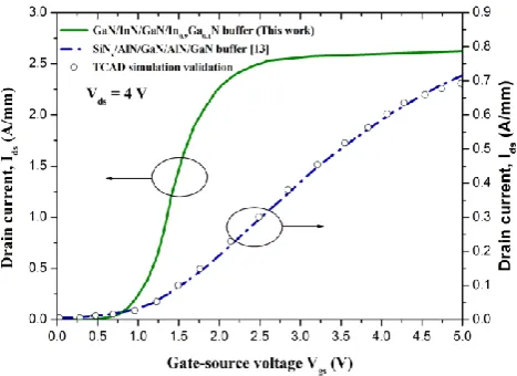
For accurate device simulation, the physical model parameters for transport model are well-matched to the reported measured data [13, 18] as shown in Fig. 2 and Fig. 3. In addition, an optimized device meshing was used to generate robust simulation structures prior to the calibration of physical models. The detailed device meshing and calibration procedure is described elsewhere [26]. The calibrated physical models are used to simulate the device described in Fig.1 and obtain different device characteristics as described below.
Fig.1 Cross-section of highly confined HfO2/GaN/InN/GaN/In0.9Al0.1N MISHEMT structure
used for numerical device simulation. Lg, Lgs and Lgd
are the gate length, S/D access region lengths, respectively. TCH, a is the channel thickness and gate
to channel distance.
Fig. 2. Experimental [13] (solid dotted lines) and simulated (symbols) transfer characteristics for AlN/GaN/AlN MISHEMT after tuning the simulation model to match the experimental curve with our InN
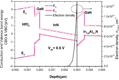
Fig. 4 shows the simulated conduction energy band diagram of the various regions of the device and electron concentration profiles in the channel under the gate for GaN/InN/GaN/In0.9Al0.1N heterostructure
MIS-HEMT for InN channel thickness (TCH = 3 nm). Under the gate, the band-diagram shows that the 2-DEG is completely depleted by the top GaN layer and the device will be normally-OFF. For the normally-OFF structure, a negative interface trap density Nit ~ - 5 ×1013 cm-2 was included at the HfO2/GaN interface
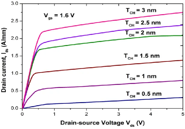
[18] which lowers the positive polarization charge. Fig. 5 shows the DC Ids versus Vdscharacteristics of the HfO2/GaN/InN/GaN/In0.9Al0.1N devices described in
section II. The saturated drain current (Ids,sat) of 2.7, 2.38, 2.09, 1.39, 0.78, 0.315 A/mm is obtained at Vgs = 1.6 V and Vds = 5 V for devices with TCH = 3, 2.5, 2,
1.5, 1 and 0.5 nm, respectively. This high value of
Ids,sat is attributed to the superior electron mobility and conductivity in the InN channel.
Fig. 6 shows the Ids-Vgs characteristics of a Lg = 100 nm InN channel MISHEMT for Vgs from -1 V to 2 V and
Vds= 0.5 V with TCH as the third parameter. The simulation data show that for TCH = 0.5, 1, 1.5, 2, 2.5 and 3 nm the values of Ids,sat are 1.17, 2.08, 2.18, 2.47, 2.52 and 2.57 A/mm, respectively. It indicates that the current through the channel will become a significant or larger component of the total drive current as the
Vgs increases. The increased current capability is due
to the presence of high mobility InN channel with high
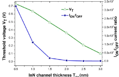
2DEG induced close to their interfaces, respectively under a 0.5 V gate bias. From Fig. 8, it has been seen that the VT begins to shift positively as the TCH decreases and device leakage current can be significantly reduced by using high-k dielectrics or thin
TCH. The proportion of the amount of the charges in the channel region controlled by the Vgs is increased.
VT increases almost linearly from 0.102 V for TCH= 3 nm to 0.728 V for TCH= 0.5 nm.
Fig. 3. Experimental [18] and simulated Ids-Vds curves
for InN channel MISHEMT with TCH = 3 nm. The gate
voltage was varied from 1.6 V to 0.6 V in step of 0.2 V.
Fig. 4. Simulated conduction energy band diagram and electron density of the device under the gate. The thickness of InN channel is TCH = 3 nm. There is relaxed 1µm In0.9Al0.1N buffer layer with GaN top and bottom
Fig. 5. Ids as a function of Vds in InN MISHEMT with various TCH measured at Vgs = 1.6 V.
Fig. 6. Simulated transfer characteristics of Ids versus Vgs (both linear and log scale) for various values of TCH in
the InN channel measured at Vds = 0.5 V.
Fig. 7 shows the variation of gm as a function of Vgs at
Vds = 0.5 V. From Fig. 7, it is found that the values of maximum gm for InN channel MISHEMT with Lg =100 nm is 2.9, 2.81, 2.76, 2.71, 2.58 and 2.44 S/mm for the values of TCH = 0.5, 1, 1.5, 2, 2.5 and 3 nm, respectively. The device with thicker channel (TCH) presents a wider current path and higher 2-DEG density, resulting in a more negative VT as well as a decreased peak transconductance [27].
An ION/IOFF ratio is a commonly evaluated merit for current technology. This ratio has a significant impact on the static power consumption in low standby power applications and higher values of the ION/IOFF ratio are desirable.
Fig. 7. Variation of gm as a function of Vgs
characteristics for various values of TCH in InN
The ON-current refers to the drive current in saturation, while OFF-current refers to the total leakage current, which is the sum of subthreshold, gate and junction leakage currents [28] extracted from
Ids–Vgs transfer characteristics at Vds = 0.5 V and Vgs= 0 V for IOFF, Vgs = 2 V for ION shown in Fig. 8. It clearly shows that ON current and OFF current is higher for device with higher TCH due to increased 2DEG along with high gate to channel separation [29]. The threshold voltage dependence on TCH is shown in Fig. 8. As seen in Fig. 8, the VT decreases with increasing
TCH for a given gate length device. As TCH increases,
VT decreases and becomes more negative due to the increased gate-to-channel distance shown in Fig 8 and achieved a maximum positive VT = 0.828 V, 0.635 V, 0.494 V, 0.360 V, 0.208 V, 0.102 V for the values of
TCH = 0.5, 1, 1.5, 2, 2.5 and 3 nm, respectively. We have also seen that VT shifts positive as the TCH is thinned down. The positive VT is desired for low-power and enhancement-mode operation.
Fig. 9 shows the ON-state resistance (RON) of device with respect to TCH. For this, the simulation was first performed to obtain the Ids-Vds characteristic in the DC mode for the values of TCH = 0.5, 1, 1.5, 2, nm with a step of 0.5 nm. The device RON extracted at Vgs = 1.6 V and Vds in the range between 0 and 0.21 V from Fig. 4. The RON of the device should be very low to reduce the power consumption in the device switching process. RON was found to decrease linearly as ns increases [30] and is given by
gd ON
s
L
R
qn
(1) where Lgd, q, ns and µ are the gate to drain access region length, the electron charge, electron sheet carrier density and mobility of the device, respectively. This causes a high device RONwith decreasing ‘TCH’ in the device. We see an increase in RONfrom a value of 0.242, 0.25, 0.277, and 0.41 Ω·mm for 2, 1.5, 1, 0.5 nm, respectively. Due to the low channel resistance of the InN channel MISHEMT, the values are low compared to what has been published so far [13,16,17].Fig. 10 shows the variation of high frequency (1 MHz)
C-V characteristics of the device for various values of
TCHwith respect to Vgs. For MISHEMT devices the total gate capacitance (Cgg) can be given as
(
) ||
||
gg ins cap gs gd
C
Series C
C
C
C
(2)where ins 0 ins ins
A
C
t
Fig. 8. Variation of VT and ION/IOFF as a function of
various TCH in InN channel measured at Vds = 0.5 V.
Fig. 9. Variation of ON-state resistance RON as a
function of TCH varying from 0.3 – 2 nm measured
from Ids-Vds characteristics at Vgs = 1.6 V.
𝐶ins is the insulator capacitance, 𝐶cap is the depletion layer capacitance comprises of GaN cap top and bottom layers with InN channel, εO is the vacuum permittivity, εins is the dielectric constant of high-K HfO2 dielectric, and A is the capacitor area. 𝐶𝑔𝑠 and 𝐶𝑔𝑑
are the gate to source and gate to drain capacitances respectively. 𝐶𝑔𝑠 and 𝐶𝑔𝑑 include the inner (𝐶𝑖𝑓) and outer (𝐶𝑜𝑓) fringing capacitances. It is noticed that there is almost negligible effect of TCH on Cgg before threshold and at strong inversion the capacitance is slightly higher for higher TCH. This is because in wider channel the carrier confinement is better which gives rise to higher Cgg [31].
The intrinsic delay time (𝜏) of a transistor is the time
taken to charge a constant gate capacitance Cgg to a voltage Vdsat a constant drain current ION[32]. The 𝜏 is a most important figure of merit because it determines the device switching speed depends on mobility and injection velocities of carriers, which are high in case of III-V materials [2] and is given as,
gg dd
ON
C
V
I
where Cgg the total gate capacitance, Vdd = Vds is the supply voltage and 𝐼ON is the ON current for various
TCH. Due to higher ION in MIS-HEMT devices, the 𝜏 will be very less and fast device switching can be achieved. Thus, MISHEMTs will have much lower Cgg, leading to the further reduction of delay. Lower values of the 𝜏
are highly desirable for logic systems and applications requiring high-performance operation [32]. Delay decreases almost linearly from 1.661 Fs for TCH= 0.5 nm to 0.761 Fs for TCH= 3 nm shown in Fig. 11. Another important figure of merit for RF application is that cutoff frequency ft and the maximum frequency of oscillation fmax which depend on the Cgg and gmof a device The ft is the frequency when the current gain is unity and is an important measure for high speed digital applications, whereas fmax is the frequency when the power gain is unity and also corresponds with the transit frequency of the maximum available power gain (MAG) that is a realistic parameter of the optimization of microwave amplifiers. The ft and fmax can be given as [33]
max
2 1 2( / )
2 ( / ) 2
2 4( )( ( / ))
m t
gs gd gs
m m
gd gs gg
m
gs s i g ds m gd gs
g F
C C C
g g
C C C
g F
C R R R g g C C
- (4)
where Cgs, Cgd and Cgg CgsCgd are the gate-to-source, gate-to-drain and total gate capacitances respectively, including fringing and overlap capacitances, gm and gds are the transconductance and output conductance, Rg,RS and Riare the gate, source and channel resistance.
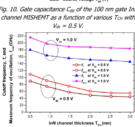
Fig. 11 show the variation of fTand fmaxfor different values of TCH of an Lg = 100 nm device. Fig. 11 clearly exhibit an increase in fT and fmax with the reduction of
TCH. This increase in fT and fmax is due to the increase in gm as TCH is scaled down. The highest values of fT /fmax observed are 98 GHz/129 GHz and 200GHz/360 GHz for Lg = 100 nm devices with TB= 0.5 nm at Vds = 0.5 V and 1.0 V, respectively. The higher ftand fmax for the thin channel device (TCH = 0.5 nm) is due to the superior gate-controllability, and hence higher gm and lowest parasitic gate capacitances compared to the thick channel (TCH = 1, 1.5, 2, 2.5, 3 nm) that results from increased gate capacitance [34].
Fig. 10. Gate capacitance Cgg of the 100 nm gate InN
channel MISHEMT as a function of various TCH with
Vds = 0.5 V.
Fig. 11. Variation of ft and fmax for various TCH with Lg
= 100 nm at Vds = 0.5 V and Vds = 1.0 V.
5. CONCLUSION
The effect of the thickness of InN channel TCH were studied and analyzed and the successful improvement of device performance of the normally-OFF operation was achieved due to the introduction of HfO2 as gate
dielectrics of the GaN/InN/GaN/In0.9Al0.1N
heterostructure. Significant increase in 2DEG, ION, gm, demonstrates the presence of high current density in the device channel material due to the presence of HfO2 dielectrics which significantly reduces the current
leakage under gate of the device. In addition, incorporation of the strain-free lattice matched In0.9Al0.1N back-barrier design in E-mode technology
biases and it can be a promising device structure for RF/power amplifier applications.
6.REFERENCES
[1] T. Palacios “Beyond the AlGaN/GaN HEMT: new concepts for high-speed transistors” Phys. Status Solidi a , vol. 206, Issue 6 , Mar. 2009, pp. 1145–8.
[2] B.E. Foutz, S.K. O’Leary, M.S. Shur and L.F. Eastman "Transient electron transport in wurtzite GaN, InN, and AlN" J. Appl. Phys., vol. 85, Isssue 11, Feb. 1999, pp. 7727.
[3] O. Ambacher, B. Foutz, J. Smart, J. R. Shealy, N. G. Weimann, K. Chu, M. Murphy, et.al; "Two dimensional electron gases induced by spontaneous and piezoelectric polarization in undoped and doped AlGaN/GaN heterostructures" J. Appl. Phys., vol. 87, Issue 1, Sep. 2000 , pp. 334.
[4] W. Terashima, S.-B. Che, Y. Ishitani, and A. Yoshikawa, “Growth and characterization of AlInN ternary alloys in whole composition range and fabrication on InN/AlInN multiple quantum wells by RF molecular beam epitaxy,” Jpn. J. Appl. Phys., vol. 45, no. 20-23, May. 2006, pp. L539–L542.
[5] E. Dimakis, E. Iliopoulos, M. Kayambaki, K. Tsagaraki, A. Kostopoulos, G. Konstantinidis, and A. Georgakilas, “Growth optimization of electron confining InN/GaN quantum well heterostructure,” J. Electron. Mater., vol. 36, no. 4, Apr. 2007, pp. 373–378.
[6] B. E. Foutz, S. K. O’Leary, M. S. Shur, and L. F. Eastman, “Transient electron transport in wurtzite GaN, InN, and AlN,” J. Appl. Phys., vol. 85, no. 11, Jun. 1999, pp. 7727–7734.
[7] M. Sumiya, K. Yoshimura, T. Ito, K. Ohtsuka, S. Fuke, K. Mizuno, M.Yoshimoto, H. Koinuma, A. Ohtomo, M. Kawasaki, "Growth mode and surface morphology of a GaN film deposited along the N-face polar direction on c-plane sapphire substrate”, J. Appl. Phys, vol. 88, Apr. 2000, pp. 1158–1165.
[8] M.H. Wong, Y. Pei, T. Palacios, L. Shen, A. Chakraborty, L.S. McCarthy, S. Keller, S.P. DenBaars, J.S. Speck, U.K . Mishra, "Low nonalloyed ohmic contact resistance to nitride high electron mobility transistors using N-face growth", Appl. Phys. Lett., vol. 91, pp. Issue 23, Dec. 2007, pp. 232103.
[9] S. Rajan, A. Chini, M.H. Wong, J.S. Speck, U.K . Mishra, “N-polar GaN/AlGaN/GaN high electron
mobility transistors” J. Appl. Phys., vol. 102, Issue. 4, Aug. 2007, pp. 044501.
[10] M.H. Wong, S. Keller, Nidhi, S. Dasgupta, D. J. Denninghoff, S. Kolluri, et.al., "N-polar GaN epitaxy and high electron mobility transistors"
Semiconductor Science and Technology, vol. 28, June, 2013, pp. 074009
[11] Nidhi, S. Dasgupta, J. Lu, J.S. Speck, and U.K. Mishra "Self-aligned N-Polar GaN/InAlN MIS-HEMTs with record extrinsic transconductance of 1105 mS/mm" IEEE Electron Device Letters, vol. 33, no. 6, June 2012, pp. 794-796.
[12] D. Denninghoff, J. Lu, E. Ahmadi, S. Keller and U. K. Mishra "N-polar GaN/InAlN/AlGaN MIS-HEMTs with 1.89 S/mm extrinsic transconductance, 4 A/mm drain current, 204 GHz fT and 405 GHz fmax" Device Research
Conference (DRC), Notre Dame, IN, Jun. 2013, pp. 197 – 198.
[13] U. Singisetti, M.H. Wong, S. Dasgupta, Nidhi, B. Swenson, B.J. Thibeault, J.S. Speck, and U.K. Mishra "Enhancement-mode N-Polar GaN MISFETs with self-aligned source/drain regrowth" IEEE Electron Device Letters, vol. 32, no. 2, Feb. 2011, pp. 137-139.
[14] Nidhi, S. Dasgupta, D.F. Brown, S. Keller, J.S. Speck and U.K. Mishra "N-polar GaN-based highly scaled self-aligned MIS-HEMTs with state-of-the-art fT.LG product of 16.8 GHz-μm"
IEEE International Electron Devices Meeting (IEDM), Baltimore, MD, Dec. 2009, pp. 1 – 3. [15] U.K. Mishra "N-Polar deep recess MISHEMTs
with record 2.9 W/mm at 94 GHz" IEEE Electron Device Letters, vol.37, Issue: 6, May. 2016, pp. 713 – 716.
[16] K. Shinohara, D.C. Regan, Y. Tang, A.L. Corrion, D. F. Brown, J.C. Wong, J.F. Robinson, et.al., "Scaling of GaN HEMTs and schottky diodes for submillimeter-wave MMIC applications" IEEE Transactions on Electron Devices, vol. 60,no. 10, Oct. 2013, pp. 2982-2995.
[17] X. Zheng, M. Guidry, H. Li, E. Ahmadi, K. Hestroffer, B. Romanczyk, S. Wienecke, S. Keller, and U.K. Mishra"N-polar GaN MIS-HEMTs on sapphire with high combination of power gain cutoff frequency and three-terminal breakdown voltage" IEEE Electron Device Letters, vol. 37, Issue: 1, Nov. 2015, pp. 77 – 80.
[18] J. Kuzmik "Proposal of normally-off InN-channel high-electron mobility transistors"
[19] D.Guerra, R.Akis, F. A. Marino, et al., “Aspect ratio impact on RF and DC performance of state-of-the-art short-channel GaN and InGaAs HEMTs,” IEEE Electron Device Letters, vol. 31, Issue: 11, Sep. 2010, pp. 1217 – 1219.
[20] J. Kuzmik "N-Polarity InN/GaN/InAlN high-electron-mobility transistors" Applied Physics Express, vol. 5, Apr. 2012, pp. 044101.
[21] TCAD Sentaurus, Sdevice User Guide, ver.G-2015 , Synopsys.
[22] L.K.F. Edwin “Characterization and numerical simulation of gallium nitride-based metal-oxide-semiconductor high electron mobility transistor with High-K gate stack”, Master thesis, Electrical and Computer Engineering, National University of singapore, Jan. 2012.
[23] S. Russo, "Gallium nitride-based device simulation and development", Ph.D. dissertation, Università di Tor Vergata, 2008. [24] O. Ambacher, J.Smart, J. R.Shealy, et al.,
“Two-dimensional electron gases induced by spontaneous and piezoelectric polarization charges in N-and Ga-face AlGaN/GaN heterostructures” J. Appl. Phys., vol. 85, Issue 6, Mar. 1999, pp. 3222.
[25] S.K. Saha, “Introduction to technology computer aided design,” in Technology Computer Aided Design: Simulation for VLSI MOSFET: C.K. Sarkar (ed.). CRC Press, Taylor & Francis, Boca Raton, USA, May 2013.
[26] M.X. Hua, Z.Y. Man, W.X. Hua, Y.T. Ting, P. Lei, C.W. Wei, and L.X. Yu "Breakdown mechanisms
in AlGaN/GaN high electron mobility transistors with different GaN channel thickness values"
Chin. Phys. B, vol. 24, no. 2, Jan. 2015, pp. 027101.
[27] H.M. Pardeshi, G. Raj, S. Pati, N. Mohankumar, C.K.Sarkar "Performance assessment of gate material engineered AlInN/GaN underlap DG MOSFET for enhanced carrier transport efficiency" Superlattices and Microstructures, vol.60, Aug. 2013, pp. 10–22.
[28] P. Å. Nilsson, H. Rodilla, J. Schleeh, N. Wadefalk, J. Grahn "Influence of gate-channel distance in low-noise InP HEMTs" International Conference on Indium Phosphide and Related Materials (IPRM), Kobe, May. 2013, pp. 1 - 2 [29] A. Raman, S. Dasgupta, S. Rajan, J.S. speck,
and U.K. MISHRA "AlGaN channel high electron mobility transistors: device performance and power-switching figure of merit" Japanese Journal of Applied Physics, vol. 47, no. 5, May, 2008, pp. 3359–3361.
[30] M.H. Alam, I. A. Niaz, I. Ahmed, Z.A. Azim, N.Chowdhury and Q.D.M. Khosru "InxGa1-xSb
MOSFET: Performance analysis by self consistent CV characterization and direct tunneling gate leakage current" International Conference on Electro/Information Technology (EIT), Indianapolis, IN, May. 2012, pp. 1-6. [31] K. Majumdar, P. Majhi, N. Bhat and R. Jammy