Advanced Ceramics Progress
J o u r n a l H o m e p a g e : w w w . a c e r p . i r
Implementation of EIS for Dopant Profile Analysis in n-type Silicon
A. Saraeia, M.J. Eshraghi*a, F. Tajabadib, A. Massoudia
aDepartment of Semiconductor, Materials and Energy Research Center, Karaj, Iran
bDepartment of Nanomaterials and Advanced Materials, Materials and Energy Research Center, Karaj, Iran
P A P E R I N F O
Paper history:
Received 18 January 2017
Accepted in revised form 09 July 2017
Keywords: ECV Depth profile Doping
A B S T R A C T
An experimental setup has been developed for successive photo-electrochemical etching and EIS measurement of semiconductor samples. Furthermore, an algorithm based on electrochemical capacitance-voltage (ECV) has been developed for calculating dopant profile based on the measurements by the developed setup. Phosphorous diffusion profile in silicon was estimated by employing the developed setup and algorithms. Measurements by proposing setup and algorithm are in good agreement with commercial ECV instrument and obtained results were compared with dopant profile-resistivity correspondence method.
1. INTRODUCTION1
Depth profile characterization is critical for obtaining optimum performance in the semiconductor device fabrication and photovoltaic industry [1]. Conventional methods for obtaining dopant profile are secondary ion mass spectroscopy (SIMS), Spread resistance measurement (SR), Sequential four point probe (FPP) and chemical etch method, capacitance-voltage (CV) and electrochemical capacitance-voltage (ECV) [2]. Among these methods, SIMS needs an expensive instrument and is not capable of measuring lateral diffusion of dopants with high resolution. In addition, SIMS application is limited to chemical doping concentration analysis [3]. FPP method requires large volume of sample for measuring dopant distribution in semiconductor [4]. In CV technique, deposition of an metal contact with sample for creating a Schottky contact is necessary [5]. The main limitation of the CV method is the electrical breakdown voltage of the sample which implies a limit on the maximum applicable reverse bias which is needed for forming space-charge region and consequent limit on depth. In addition, in the CV method, we need a high field for characterizing low-doped regions which is in contrast to sample electrical breakdown voltage [6]. In Electrochemical capacitance-voltage (ECV) method,
1
*Corresponding Author’s Email: [email protected] (M.J. Eshraghi)
Schottky contact is formed by an electrolyte solution instead of a metallic contact. The successive etching of the sample surface and CV measurement in electrolyte enable us to overcome the depth limitation of the CV method [7]. CV measurement is performed in reverse bias and etching sequence is done in forward bias. Other advantages of the ECV method include providing information only about the electrically active species concentration and sub-nm depth resolution. In this method, the capacitance is measured with respect to suitable applied voltage. The applied voltage is chosen in a part of the IV curve in which minimum current has been crossed through the sample and no etching occurred during this process. In next step, the sample is etched in predetermined duration and controlled conditions. This cycle will be repeated frequently and data will be collected for future analysis. At each step, doping concentration is obtained bydifferentiating 1/C2 over the V and applying the Eq. 1. The depletion region depth is calculated by using Eq. 2 [8].
N(W ) = (1)
W = (2) Where q is charge of electron, 0 is the permittivity of vacuum, r is the relative permittivity of the semiconductor material and A is the exposed surface area of the sample in the electrolyte. Then etched depth
is obtained by integration of current over time and applying the Eq. 3.
W = ∫ Idt (3) Where M is the Semiconductor molecular weight, Z is the charge transferred per molecule dissolved, F is the Faraday constant and ρ is the density of the semiconductor. Finally, by using the Eq. 4 total depth will be obtained [10].
X = W + W (4)
Although commercial instruments are available for obtaining the dopant profile based on ECV method, their price is high and they are not available in many labs. On the other hand, potentiostats with electrochemical impedance spectroscopy (EIS) module are available in many labs so implementing ECV technique by potentiostats equipped with EIS module could help many researchers investigate the dopant profile with their available instruments. The main aim of this research is development of simple setup and algorithm for dopant profile measurement in silicon semiconductors based on ECV technique by using a potentiostat equipped with EIS module. To best of our knowledge, there is no report about carrying out such measurement with conventional potentiostat.
2. EXPERIMENTAL
P-type silicon wafers (100) with the resistivity of about of 0.12 Ω.cm and thickness of 440 μm and boron dopant density of 1.88×1017 cm-3 were used as base material. Wafers surface were cleaned by immersion in a solution of HF/CH3COOH/HNO3 with 2/5/15 volume ratio. Diluted phosphoric acid was used as a phosphorus source. The Aqueous solution of phosphoric acid with spraying rate of 5.2 g/min was sprayed over silicon wafers. According to chemical reactions 5 and 6, the phosphoric acid will be dehydrated and finally would be decomposed to yield phosphorus [11].
2H3PO4 → 3H2O+ P2O5 (5)
2P2O5 + 5Si→ 5SiO2 + 4P (6) Phosphoric acid concentration is chosen based on the Eq. 7 which is equal to P2O5 wt%. In this work, 15 wt% P2O5 was selected based on Eq. 7.
P2O5 wt.% = 0.7242× (weight of H3PO4) / (weight of H3PO4 + weight of H2O) (7) After spraying, the samples were dried in an oven at 200°C for 10 minutes. The phosphorus diffusion process was done in a furnace under N2 (99.999%) and O2 (99.99%) atmosphere and with flow rate of 1 L/min and 20 cc/min, respectively, at 910°C for 47 minutes. Four samples with the same condition have been prepared to be used in the different analysis. Dopant profile was
measured by sequential sheet resistance measurement in FPP configuration and etching in 20% KOH solution at 25°C for time periods of 20 s to 160 s. Etched depth was calculated based on etch rate and etch duration. The dopant concentration has been evaluated from the correspondence of sheet resistance and dopant concentration curves according to reference [12]. In addition, ECV profiler equipped with Polaron Profile Plotter model PN4100 and Bio-Rad PN4200 was used for comparison.
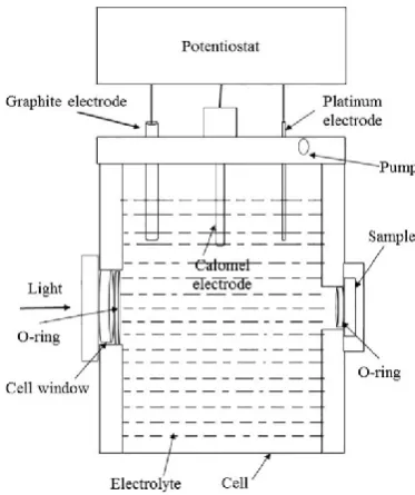
In the developed setup, the semiconductor is in contact with an electrolyte solution (NH4F 0.1M) and a region around 0.28 cm2 of the sample surface is exposed to the electrolyte. The setup is configured in such a way that during the etch process, the sample surface could be illuminated by UV-light which is necessary to generate carriers in n-type semiconductor to perform the etch process. In the developed setup, a saturated calomel electrode and a platinum electrode and a graphite electrode are used as a reference, counter electrode for measuring CV and counter electrode for etching, respectively. The dopant profile measurement begins by CV measuring and is followed by etching the sample. By reducing the etch duration, measurement accuracy could be increased to depths below the 100 nm [13]. Fig. 1, shows a schematic image of the developed experimental setup.
Figure 1. Fabricated electrochemical cell.
3. RESULT AND DISCUSSION
sheet resistance is measured after each etching experiment and was multiplied by a correction factor (4.53) and then conductivity was calculated. The conductivity differences between each two adjacent steps were calculated and obtained results are reversed to find the values in the fifth column of Table 1 as resistivity. Resistivity values are converted to concentration according to reference [12]. Finally, Etch depth at each step has been obtained by multiplying Etch rate in etch time.
TABLE 1. Calculation of concentration by FPP method.
Etch time (s)
RS
(Ω/sq)
Total etched depth (μm)
1/∆G (Ω)
1/∆G×∆ X×10-4
(Ω.cm) N (cm-3)
0 23.1 0 ― ― ―
20 25.6 0.022 1078 2.3×10⁻³ 3×10¹⁹
40 35.7 0.066 412 1.8×10⁻³ 4×10¹⁹
60 15.3 0.132 122 8×10⁻⁴ 9×10¹⁹
80 17.2 0.220 631 5.5×10⁻³ 1019
100 17.8 0.330 2326 2.5×10⁻² 8×10¹⁷
120 18.18 0.462 3883 5.1×10⁻² 2×10¹⁷
140 17.8 0.616 3883 5.9×10⁻² 1×10¹⁷
160 17.2 0.792 2326 4×10⁻² 3×10¹⁷
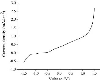
Fig. 2 indicates the I-V curve of a doped sample. This graph clearly shows the anodic behavior of silicon, which depends on the applied voltage. In addition, it can be seen that in a potential value of 1.5 V, current reaches a saturation value which is proportional to illumination intensity. This value corresponds to the lowest current for generating holes by photo-excitation and gives us capability to control the etch rate of silicon [14]. The sample has been etched by applying current and the current change during time has been recorded as I-T curves at an etch voltage of 1.5 V and under UV-illumination.Bias voltage range for CV measurement is chosen in such a way that conductance is minimum and capacitance changes gradually with a bias voltage. According to Fig. 2, the current in a potential range of -0.3V to -0.1V is minimum, therefore the CV measurement is performed in the aforementioned potential range to avoid unwanted specimen etch [15]. For a more accurate determination of potential bias range, the CV profile of diffused sample in the electrolyte has been obtained in the estimated range of -0.3 V to -0.1 V. Based on the CV profile of diffused sample shown in Fig. 3, capacitance change with bias
voltage is minimum in the bias voltage range of -0.12 V to -0.1 V, therefore this range has been selected for the CV measurement experiments.
Figure 2. I-V curve of doped silicon.
Figure 3. Moth Schottky curve of the diffused sample.
duration in which the sheet resistance slope was reversed according to Fig. 4 and in a solution of HF/H2O with 1/10 volume ratio. Fig. 4 shows that with etching the sample for 30 s, the dead layers have been removed completely from sample surface.
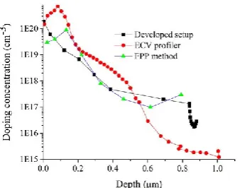
This procedure is the reason of difference in the results of commercial ECV and our proposed method. R-squared values which are obtained with commercial ECV and developed setup are 0.3305 and 0.3401, respectively. The junction depth of dopant which was evaluated based on sequential etch and sheet resistance measurement method is around 550 nm at a concentration in order 1017 cm-3 (Fig. 5). Also, FPP method measures doping concentration value until reaching the p-n junction, which is about 1017cm-3 based on feedback concentration and ECV profile method measures electrically active concentration, therefore these two different methods consider formation of their profile after diffusion depth in part of the p-n junction.
Figure 4. Removing dead layer curve of the sample.
Figure 5. Characterization of diffused phosphorus in silicon.
4. CONCLUSIONS
Diffusion of Phosphorous in P-type Silicon wafers has been done by spraying liquid source and performing diffusion process at 910°C for 47 min.
A measurement setup and algorithm for measurement of concentration profile of diffused phosphorus in silicon based on sequential controlled electrochemical etching and electrochemical impedance spectroscopy by using a
potentiostat was developed. Diffusion profile of diffused sample was measured by a commercial ECV instrument and our algorithm shows good agreement with 9.64% error. The results of proposed method showed that diffusion depth of the sample is around 500 nm. This value is confirmed by etching and surface resistivity measurement which is frequently used.
5. ACKNOWLEDGLEMENT
The authors would like to thank the members of the semiconductor department of Materials and Energy Research Center in Karaj.
REFERENCES
1. Werner, S., et al., "Doping-and carrier concentration profile characterisation of highly phosphorus-doped emitters", EU PVSEC, Valencia, Spain, (2010).
2. Bock, R., Altermatt, P.P. and Schmidt, J., "Accurate extraction of doping profiles from electrochemical capacitance voltage
measurements", European Photovoltaic Solar Energy
Conference, Vol. 1, No. 5, (2008).
3. Álvarez, D., Hartwich, J., Kretz, J., Fouchier, M. and
Vandervorst, W., "Scanning Spreading Resistance Microscopy for the characterization of advanced silicon devices",(2003).
4. Dickey, D. and Brennan, R., "Determination of Diffusion
Characteristics Using Two-and Four-Point Probe
Measurements",Solid State Technology, Vol. 27, (1984), 125-132.
5. Dragicevic, M., Bergauer, T., Hrubec, J., Krammer, M.,
Treberspurg, W. and Valentan, M., "Comparing Spreading Resistance Profiling and CV characterisation to identify defects in silicon sensors", Journal of Instrumentation, Vol. 8, (2013), 02018.
6. Sell, B., Gatzke, C. and Fernandez, J., "Electrochemical capacitance-voltage profiling of heterostructures using small contact areas", Semiconductor Science and Technology, Vol. 13, No. 4, (1998), 423.
7. Kinder, R., "Profiling of the p–n Junction in Silicon by the
Electrochemical Capacitance–Voltage Technique", physica
status solidi (A), Vol. 169, No. 2, (1998), 261-265.
8. Hashima, U.,Bajuri, S.N.M., Abdul Halim, N.H., Majlis, B.Y.,
"Shallow junction determination and boron profiling using electrochemical capacitance-voltage (ECV)" Jurnal Fizik Malaysia, Vol. 30, (2009), 37-42.
9. Ambridge, T., Stevenson, J.L. and Redstall, R.M., "Applications
of Electrochemical Methods for Semiconductor
Characterization I. Highly Reproducible Carrier Concentration Profiling of VPE “Hi‐Lo”", Journal of the Electrochemical Society, Vol. 127, No. 1, (1980), 222-228.
10. Hulenyi, L., Kinder, R. and Satka, A., "Determination of implanted layer depth in silicon by electrochemical CV
technique", Advanced Semiconductor Devices and
Microsystems, (2000), IEEE.
11. Kim, D.S., Hilali, M.M., Rohatgi, A., Nakano, K., Hariharan, A. and Matthei, K., "Development of a phosphorus spray diffusion system for low-cost silicon solar cells", Journal of the Electrochemical Society, Vol. 153, no. 7, (2006), 1391-1396. 12. Sze, S.M. and. Ng, K.K., "Physics of semiconductor devices",
(2006), John wiley & sons.
13. Yakovlev, G., Frolov, D.S., Zubkova, A.V., Levina, E.E.,
Zubkov, V.I.,Solomonov, A.V., Sterlyadkin, O.K. and Sorokin,
Structures by Electrochemical Capacitance–Voltage Profiling", Semiconductors, Vol. 50, No. 3, (2016), 320-325.
14. Muddasani, A., "Determination of carrier concentration in GaN/AlGaN nanostructures using electrochemical capacitance-voltage profiling", (2007), ProQuest Dissertations Publishing.