Header for SPIE use
Parallel confocal laser microscope system using smart pixel arrays
Makoto Naruse
∗and Masatoshi Ishikawa
Department of Mathematical Engineering and Information Physics,
Graduate School of Engineering, University of Tokyo
7-3-1 Hongo, Bunkyo-ku, Tokyo 113-8656 Japan
ABSTRACT
The temporal resolution of a confocal laser microscope, by which three-dimensional data of specimens are obtained, usually suffers the slow speed of image acquisition devices, such as CCDs, or scanning mirrors. Here we propose a confocal microscope system where parallel optoelectronic devices are employed aiming at obtaining high frame rate of three-dimensional data that provides real time analysis of dynamical properties and adaptive feedback control of the specimen. A smart pixel yields pixel-parallel data processing capability owing to its integrated optical devices and electronic processing circuits fabricated on a same chip. A vertical-cavity surface-emitting laser (VCSEL) array is introduced for the parallel probing beams by which the optical system is simplified. In addition, pixel parallel illumination control is achievable. We have performed basic experiments on a system composed of an 8x8 VCSEL array, a silicon photodetector array, and processing element (PE) array. Each PE contains an arithmetic logic unit (ALU), 24-bit local memory, and electrical connections to neighboring pixels, that provides fast processing versatility such as the moving object recognition. Vibrating a sample by a piezo micro stage, we have successfully obtained a dynamical property, which is a one-dimensional moment of the moving sample, on the basis of the data obtained by the experimental system over the range of conventional video frame rate.
Keywords: Confocal laser microscope, integrated optical devices, smart pixels, vertical-cavity surface-emitting laser (VCSEL), optoelectronic LSI
1. INTRODUCTION
The confocal laser microscopes have been one of the most important tools for biology, physiology, diagnostic pathology, or material sciences by which out-of-focus blur is eliminated giving the capability of direct non-invasive serial optical sectioning of intact and even living specimens [1][2]. It is possible to obtain three-dimensional (3D) data of thick transparent object such as biological cells and tissues. Owing to the progress of the lasers, photo sensors, scanning mechanical systems, and digital image processing systems, even 3D animation of confocal images has been obtained. However, the temporal resolution tends to be limited by the frame rate of image acquisition devices such as CCDs or beam scanning mirrors. Several “real-time” confocal laser systems have already appeared but the definition of “real-time” is typically that the one frame acquisition is done in 33msec, which is the standard of the video signal transfer specification. This fact, in turn, indicates that as far as CCD or slow mechanical system has been used, it is difficult to obtain data faster than 33msec cycle time. In addition to the data gathering process, for the adaptive reaction to the specimen, computational procedure must be required after sufficient data is obtained. Therefore for the very fast phenomena, both data acquisition and data processing must be finished quickly.
Concerning these issues, this paper proposes a parallel confocal laser microscope system that is based on optoelectronic parallel integrate devices [3][4] to enhance the temporal resolution of confocal systems as well as providing some new capabilities such as pixel parallel illumination control.
The architecture and features of the system is shown in section 2. The benefits reaped by smart pixels are summarized in section 3. In section 4, the introduction of VCSELs is discussed. Section 5 describes the experiments and section 6 concludes the paper.
∗
Correspondence: Email: [email protected] Phone: +81.3.5841.6937 Fax: +81.3.5841.6952 URL: http://www.k2.t.u-tokyo.ac.jp/
2. PARALLEL CONFOCAL MICROSCOPE SYSTEM USING INTEGRATED OPTOELECTRONIC DEVICES
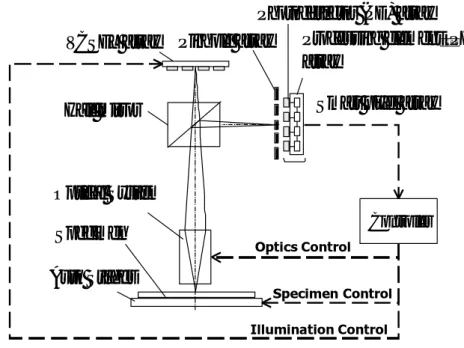
The schematic diagram of the proposed system is shown in Fig. 1. Basically, this system has two main features.
Firstly, a new data acquisition device, which is a so-called “smart pixel”, has been introduced replacing the conventional CCDs, as shown in Fig. 1. A smart pixel is basically an optoelectronic large-scale integrated circuit (LSI) that has both computational capability and optical communication channels. It has been developed for optical interconnects applications where smart pixel arrays take advantage of their aggregated communication bandwidth. For confocal microscopic applications, the pixel parallel optical power detection and computational capability greatly improve the confocal image acquisition and processing performance. By this physical device characteristic, the system could have real time data analysis and adaptive control capability. For example, by controlling the optical system or specimen based on the sequence of data given to a smart pixel chip, we can track a specific target area, for instance a cell in a tissue for biological application, that moves very quickly which could not be traced by conventional 33msec system.
Secondly for optical light sources, a vertical-cavity surface-emitting laser (VCSEL) [5] has been introduced. This device is also typically developed for optical interconnections where VCSELs provide densely parallel optical beams that are emitted vertically to the surface of the chips. Owing to their physical nature, no optical system is required to obtain two -dimensional array of optical beam. In addition, each optical output channel is individually controlled. In other words, pixel parallel individual illumination control is achievable so that the dynamic range of the photodetector is maximized.
In the following two sections, these two items are discussed. .
VCSEL array
Half mirror
Optical System
Specimen
Auto Stages
Photodetector (PD) array
Pinhole array
Controller
Processing element
(
PE)
array
Smart pixel array
Optics Control Specimen Control Illumination Control
Figure 1. Parallel confocal microscope system using integrated optical devices.
3. PARALLEL DATA ACQUISITION AND PROCESSING
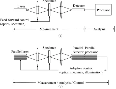
To obtain the information of each sampling point in a given specimen using a confocal laser microscope, either optical system or specimen has to be scanned so that the beam from the laser covers the target area. After data acquisition procedure, a computer that is connected to the photodetector reconstructs three-dimensional data. This conventional system
configuration is depicted in Fig. 2(a), where measurement stage and data analysis process are separated. The frame rate of confocal image is limited by the data transfer mechanism from a photodetector to a computer. Since most of two -dimensional array sensors such as CCDs are using video-signal for their standard data transfer methods, the number of image obtained during one second is typically only 30 frames. Two -dimensional data have to be converted to serial one-dimensional data. As one of the methods to increase the sampling points that can be simultaneously detected, a parallel beam system based on the Nipkow disc, which generates array of spots, has been developed. However, as far as scanning based sensors such as CCDs has been used, the advantage of parallel beams does not yield faster frame rate. Moreover, together with the data processing procedure, it takes more time to process an confocal image.
In addition, we have to note that the control of scanning mechanism is basically applied in a feed-forward way, which means that adaptive action is almost impossible on the basis of the obtained confocal data. The word “real-time” has been used in some of the work related to confocal microscopic systems, but it typically means that confocal image acquisition process is done in 30 frames per second.
In contrast to this, proposed system is modeled as shown in Fig. 2(b) where data parallel measurement and processing is realized by a smart pixel array. Owing to the computational capability that is given to each photodetector, pixel parallel data processing is performed. Based on computed data, optical system, specimen or illumination could be adaptively controlled. In other words, in the proposed system, three main procedures (measurement, data analysis, and control) are mixed or merged, where a “feed-back” control is available. This indicates that new computational paradigm is required so that intended applications are to be efficiently implemented into either smart pixel arrays or the host computer, whereas in conventional system all digital processing loads is performed at the host computer only where usual signal processing theories could be directly applied.
Laser Detector
Specimen
Processor
Feed-forward control (optics, specimen)
Measurement Analysis
Adaptive control (optics, specimen, illumination)
Measurement / Analysis / Control Parallel laser
Parallel detector
Parallel processor Specimen
(a)
(b)
Figure 2. The architecture of conventional confocal laser microscopes (a) and a new paradigm (b).
As in the case of typical conventional confocal system, threedimensional data is to be obtained by summing up the two -dimensional sectioning data. Suppose three--dimensional sampling points in a specimen are separated into N×N×N pixels. The information of each sampling point, X(x, y, z), is obtained serially as s(t)=s(x+yN+zN2) if the scanning along three axes is to be performed in the order of x, y, and z. Eventually, it needs the order of N3 for data acquisition time. The dataset s(t) is stored in the memory of a host computer in which all computational procedure is to be performed.
In contrast to this, the proposed system basically needs scanning along z direction. The signal is detected as )
, , ( ) , ,
(x yt X x yt
s = . Therefore to obtain whole data, the time frame is in the order of N. If all data is contained in the local memory of the pixel, pixel parallel computation could be performed within smart pixel chip. There is no need to transfer the data s(x, y, t) to the host computer. In other words, three-dimensional data is stored in a chip that contains photodetector on the same LSI die. Using this characteristic, a novel target-tracking algorithm has been proposed [6] that takes advantage of the fact that target objects do not move more than one-pixel due to the fast frame rate.
4. VCSEL-BASED PARALLEL PROBING 4.1 VCSEL as the Light Source
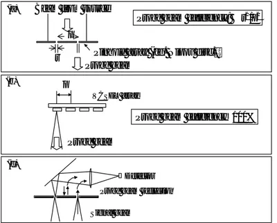
The VCSEL has itself several notable features such as low threshold current, low power dissipation, high efficiency, and circular beam emission. These features are directly applied to confocal laser microscope system applications. The VCSEL itself can be the source of the confocal laser system, whereas in conventional system, several lenses are required to make the small source of a probing beam. By the use of two-dimensional VCSEL array, parallel beams are formed without complicated optical system as the case of Nipkow disc setups. Figure 3 shows basic structure of Nipkow disc oriented system. Since there are typically no correlations between individual channels there are no interferences among parallel beams. In the case of very densely VCSEL array, however, phase equalization between channels has been reported, which indicates that there is a possible technological limitation for the density of parallelism.
In addition to the simplification of optical system, the efficiency of the usable optical power as probing beams is better than multiple pinhole based systems. Here we roughly compare the efficiency. For the pinhole array based system, the total amount of optical power that could pass the pinhole is roughly evaluated as r2/p2, where r means the diame ter of a pinhole and p is the pitch between two pinholes, as shown in Fig. 4(a). Most of optical power from the source laser is not used as the probing beams. If the power of each beam should be enlarged, we need more powerful laser source. In the case of VCSEL, all of the light emitted from a single VCSEL could be a probing beam, as shown in Fig. 4(b). In this sense, the efficiency is 100%.
Additionally, in the case of Nipkow disc system, the signal to noise ratio of the detected light is another problem. Some of the light from the source laser reflects at the surface of the disc, which eventually could be detected by the sensor as noise, as shown in Fig. 4(c). In the proposed system no such problem occurs.
Nipkow disc Light source
Objective
Specimen
Detector
Probe beam efficiency: r2/p2 Beam from source
Pinhole array (eg. Nipov disc.)
p r (a)
Signal beam
Probe beam reflection (c)
Probe beam efficiency 100%
p
VCSEL array
Probe beam
(b)
Probe beam
Detector
Figure 3. Basic configuration of Nipkow disc based
4.2 Pixel Parallel Illumination Control
Each channels of the VCSEL could be controlled independently; illumination could be individually controlled depending on the status of the specimen. Therefore, the dynamic range of the photodetector and the analog-to-digital converter could be adaptively configured to be its maximum range. As the time frame of one signal sampling time shortens, the number of photon that is detected decreases, which deteriorates the signal to noise ratio. To avoid this, the power of beam could be configured so that enough photons could be transferred to the photodetector so that the information of the specimen is properly obtained.
Suppose that the intensity of the light illuminating a point (x, y) is written by L(x,y). Let R(x, y) be the transmission of the sampled point. Then, the optical power detected by the corresponding photodetector S(x, y) is given by
).
,
(
)
,
(
)
,
(
x
y
L
x
y
R
x
y
S
=
(1)If the dynamic range of the specimen at the sampling point (x, y) is given by
max min
(
,
)
(
,
)
)
,
(
x
y
R
x
y
R
x
y
R
≤
≤
(2)then, in order to use full dynamic range of the photodetector and post detector circuits, configure L(x, y) so that the sensitivity given by
)
,
(
)
,
(
y
x
R
y
x
S
∂
∂
(3)is maximized in this range. To calculate the L(x, y), the local computational capability and local memory given to each smart pixel could be used, which indicates that the pixel parallel illumination could be performed very fast. Figure 5 summarizes the idea of pixel parallel illumination control scheme.
VCSEL array
Specimen
Physical parameter range
Photodetector dynamic range
Actual intensity distribution R(
x , y ) Illumination Control ) , (x1 y1
L L(x2,y2)
) , (x1 y1 R
) , (x2 y2 R At ( x1 , y1 ) At ( x2 , y2 )
5. EXPERIMENT
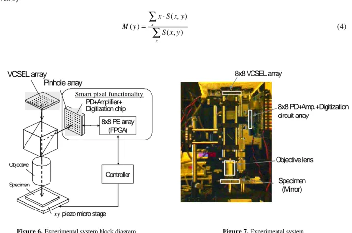
To confirm the basic principles of the parallel laser microscope system, we have constructed an experimental system. Figure 6 and 7 shows the block diagram and the photograph of the system, respectively.
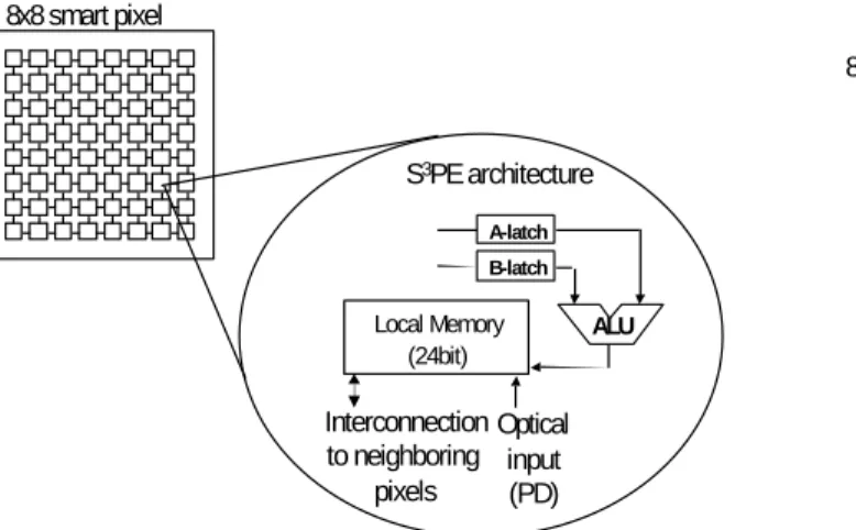
An 8x8 VCSEL array operated at the wavelength of 850nm has been used as the parallel light source. The aperture of each VCSEL is 15µm diameter, and the full divergence angle is around 10 degree. The output optical power is around 2mW for 15mA driving current. The pitch is 250µm. As the smart pixel chip, we have an equivalent functionality by combining a photodetector array chip and a processing element array device. As photo sensors, an 8x8 silicon photodetector array to which 64-channel parallel amplifier and digitization circuits are monolithically integrated. Figure 8 shows the photograph of the 8x8 photodetector chip. Four sets of 16-ch post detector circuit are located around the 8x8 photodetector array. The sensitivity of the PD is 0.1A/W for 850nm beam, and the transimpedance gain is 150Ω. It has been successfully operated up to 10Mbit/s [7]. The processing element has the S3PE architecture where each pixel has 24-bit local memory, 1-bit arithmetic logic unit (ALU), 4-neighbor connections, and a photodetector input. Owing to the existence of the local memory and electronic connections to neighboring pixels, three-dimensional processing is efficiently performed. An 8x8 PE has been integrated into a field programmable gate array (FPGA) device which is an Actel’s A32200DX having 20,000 gate and work at 225MHz. The 8x8 PE consumes 48.76% of the overall logic gate on this FPGA device. The objective lens is a Spindler & Hoyer x20 microscope objective lens.
To confirm the basic property of the system, the specimen is a plane mirror with refraction of 80%. In addition, the pinhole array is omitted. In this basic experimental setup, substantial amount of light is lost due to the mismatch of the source beam from VCSEL to the aperture of the objective lens, only 4.8% light is falling on to the specime n. And the total amount of light that could be reached to a photodetector is 1.1% of the original optical power. The uniformity of the parallel beam is 39% of the average optical power.
As an example of high-speed data processing, one-dimensional moment has been derived from the photodetector signal that is given by
∑
∑
⋅= x x
y x S
y x S x y
M
) , (
) , ( )
( (4)
8x8 PE array (FPGA) PD+Amplifier+ Digitization chip
VCSEL array
Specimen
xypiezo micro stage Pinhole array
Objective
Controller
Smart pixel functionality
8x8 PD+Amp.+Digitization circuit array
8x8 VCSEL array
Specimen (Mirror) Objective lens
where S(x, y) represents a confocal image. The specimen is a plane mirror whose edge is detected by confocal microscopy that results in the difference of 1D moment. When the specimen is intentionally vibrated by a piezo micro stage up to 60Hz, the 1D moment is successfully obtained as shown in Fig. 10. Here, the edge of the plane mirror is detected as the value of 1D moment since the difference of the mirror’s thickness is measured by confocal optical setups. In this experiment, PE array is operated at 400Hz clock frequency due to the controller’s specification. But as already shown, the PD and PE array could work up to 10MHz.
Local Memory (24bit)
A-latch B-latch
Interconnection to neighboring
pixels
Optical input (PD)
ALU
S3PE architecture
8x8 smart pixel
16ch amplifier and digitization circuit array 8x8 photodetector array
16ch amplifier and digitization circuit array
Figure 8. Experimental system block diagram. Figure 9. Photodetector array.
One-dimensional moment
∑
∑
⋅
)
,
(
)
,
(
y
x
S
y
x
S
x
Figure 10. One-dimensional moment extraction for moving specimen.
6. CONCLUSION
A parallel confocal laser microscope system using integrated optoelectronic devices such as smart pixels and VCSELs has been proposed. The frame rate of confocal image acquisition and processing is greatly enhanced owing to its parallel architecture. In addition, the use of the VCSEL array, two -dimensional probing beams is efficiently produced. Moreover,
pixel parallel illumination control is achievable. The existence of local memory and computational capability just after data acquisition device provides interactive or adaptive sensing mechanism into the confocal microscopy. The experimental system verifies the parallel confocal measurement capability and a feature value, one-dimensional moment, has been obtained.
Further investigation is now being performed: theoretical and technological limitation analysis, practical adaptation to real confocal applications, and some other topics.
ACKNOWLEGEMENT
The authors thank NTT photonics laboratories for providing the VCSEL array and Hamamatsu Photonics K.K. for the photodetector array.
REFERENCES
1. C.J.R. Sheppard and D.M. Shotton, Confocal laser scanning microscopy, BIOS Scientific, Oxford, 1997.
2.
J. B. Pawley ed., Handbook of biological confocal microscopy, Plenum Press, New York, 1995.3. M. Ishikawa and N. McArdle, “Optically Interconnected Parallel Computing Systems,” IEEE Computer, 31, pp. 61-68, 1998.
4.
T. Komuro, I. Ishii, and M. Ishikawa, “General-purpose vision chip architecture for real-time machine vision, ” Advanced Robotics, 12, pp. 619-627 (1999)5.
H. Soda, K. Iga, C. Kitahara, and Y. Suematsu, “GaInAsP/InP surface emitting injection lasers,” Jpn. J. Appl. Phys., 18, pp. 2329-2330, 1979.6.
I. Ishii and M. Ishikawa, “Self Windowing for High Speed Vision,” IEEE Int. Conf. Robotics and Automation (Detroit, 1999.5.13), Proceedings, pp.1916-1921, 1999.7. M. Naruse, H. Toyoda, Y. Kobayashi, D. Kawamata, N. McArdle, A. Goulet, and M. Ishikawa, “An Optically
Interconnected Pipelined Parallel Processing System: OCULAR-II,” in Optics in Computing 2000, R. A. Lessard and T. Galstian, eds., Proc. SPIE, 4089, pp.440-448, 2000.