43
INVESTIGATION OF N TYPE CU2O AND SE2 LAYER
PREPARATION BY LOW COST CHEMICAL METHOD
Stephen Raja John Britto
Email ID: [email protected]
ABSTRACT: - Solar energy is considered as the most promising alternative energy source to replace
environmentally distractive fossil fuel. Solar energy is radiant light and heat from the sun harnessed using a
range of ever-evolving technologies such as solar heating, solar photovoltaics, solar thermal energy, solar
architecture and artificial photosynthesis. A solar cell, or photovoltaic cell, is an electrical device that converts
the energy of light directly into electricity by the photovoltaic effect. Solar cell based on thin-film technology.
Clearly, The thinness of the cell is the defining characteristic of the technology. Thin-film solar cell
manufacturers building their solar cells by depositing several layers of a light-absorbing material, a
semiconductors on to a substrate -- coated glass, metal or plastic. The materials used as semiconductors don't
have to be thick because they absorb energy from the sun very efficiently. As a result, thin-film solar cells are
lightweight, durable and easy to use. There are three main types of thin-film solar cells, depending on the type
of semiconductor used: amorphous silicon (a-Si), cadmium telluride (CdTe) and copper indium gallium
deselenide (CIGS). Amorphous silicon is basically a trimmed-down version of the traditional silicon-wafer cell.
As such, a-Si is well understood and is commonly used in solar-powered electronics. However, it is a
challenging task to develop solar energy converting devices using low cost techniques and environmentally
friendly materials. This paper investigates the low cost method for the production of the CIGS layer in the thin
film production process.
Key words: Solar cell, CIGS, CdTe, Electro deposition.
I.INTRODUCTION
Photovoltaic, or PV, refers to the conversion of light energy into electricity using electronic devices called solar cells. Solar cell is Unlike silicon-wafer cells, which have light-absorbing layers that are traditionally 350 microns thick, thin-film solar cells have light-absorbing layers that are just one micron thick. A micron, for reference, is one-millionth of a meter (1/1,000,000 m or 1 µm). . A number of methods exist for thin film deposition, that range from simple thermal evaporation over
multi source evaporation, physical and chemical vapour deposition to electrochemical, plasma based and hybrid techniques.
II.OBJECTIVE:
44
devices is cadmium sulfide (CdS), although zinc is sometimes added to improve transparency. Adding small amounts of gallium to the lower absorbing CIS layer boosts its bandgap from its normal 1.0 electron-volts (eV), which improves the voltage and therefore the efficiency of the device. This particular variation is commonly called a copper indium gallium diselenide or "CIGS" PV cell. Solar cells based on these materials are also very stable, thus allowing long operational lifetimes. The preparation of a thin film solar cell is a multistage process where every step affects the resulting cell performance and the production cost. CuInSe2 and other Cu chalcopyrites can
be prepared by a variety of methods, ranging from physical vapor deposition methods such as evaporation and sputtering to low-temperature liquid phase methods such as electro deposition.
III. Different types materials used in thin films are amorphous silicon (a-Si), CIGS/CIS and CdTe.
3.1 Amorphous silicon (a-Si): most common and developed. It is the non-crystalline form of silicon. The cell structure has a single sequence of p-i-n layers. When exposed to sun, their power output is significantly decreased. A-Si type thin film solar cells are commonly found in calculators. A-Si type thin film is manufactured in 6 steps. First the glass substrate is coated with a TCO (transparent conductive oxide) layer as front contact, followed by P1 laser scribing. Then a layer of
a-Si is deposited followed by P2 laser scribing. Then a metal conductive layer is placed as back contact with the relative P3 laser scribing.
Figure 3.1Amorphous silicon (a-Si)
3.2 CIGS/ CIS: it is the semiconductor material composed of copper, indium, selenium, and/or gallium. In thin film technology, CIGS has the highest PV conversion efficiency. CIGS/CIS has similar manufacturing process as a-Si thin films. However, as opposed to a-Si thin film, the glass substrate on CIGS/CIS is at the rear instead of the front. In addition, Cds is applied as a buffer layer.
Figure 3.2 CIGS (Copper indium gallium (di) selenide)
45
with an additional Cds layer for buffer. First Solar is the largest manufacturer.
IV.CIGS (Copper indium gallium (di) selenide)has an extremely high absorptivity, which means that 99% of the light shining on CIGS will be absorbed in the first micrometer of the material.
CIGS (Copper indium gallium (di) selenide) CIGS is a I-III-VI2 semiconductor material composed of copper, indium, gallium, and selenium. The material is a solid solution of copper indium selenide (often abbreviated "CIS") and copper gallium selenide. It has a chemical formula of CuInx Ga(1-x)Se2 CIGS is a tetrahedrally bonded semiconductor, with the chalcopyrite crystal structure, and a abandgap varying continuously with x from about 1.0eV (for copper indium selenide) to
about 1.7eV (for copper gallium selenide).
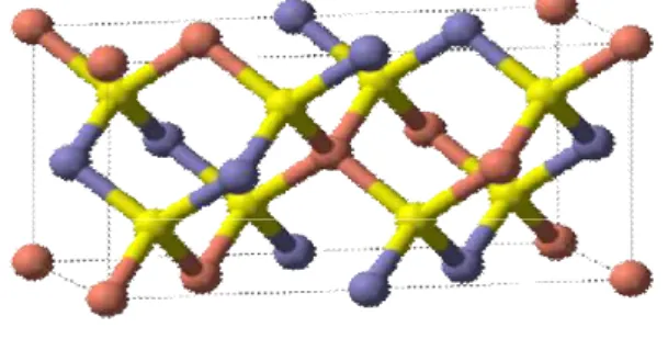
Figure 4.1 CIGS unit cell Red = Cu, yellow = Se, blue = In/Ga
CIGS is a tetrahedrally bonded semiconductor, with the chalcopyrite crystal structure. Upon heating it transforms to the zinc blende form and the transition temperature decreases from 1045 °C for x=0 to 805 °C for x=1. They are manufactured by depositing a thin layer of copper, indium, gallium and
selenide on glass or plastic backing, along with electrodes on the front and back to collect current. Because the material has a high absorption coefficient and strongly absorbs sunlight, a much thinner film is required than of other semiconductor materials.
CIGS has an exceptionally high absorption coefficient of more than 105/cm for 1.5eV and higher energy photons. CIGS solar cells with efficiencies around 20% have been claimed by both the National Renewable Energy Laboratory (NREL) and the Zentrum für Sonnenenergie und Wasserstoff Forschung (ZSW), which is the record to date for any thin film solar cell.
4.2 STRUCTURE
Table 4.2 Properties of CIGS CAS number 12018-95-0(CuInSe2)
Molecular formula
CuInxGa(1-x)Se2
Density ~5.7 g/cm3
Melting point 1070-990 °C(x=0–1) Band gap 1.7–1.0 eV (x=0–1) Crystal
structure
tetragonal
Space group I42d Lattice
constant
46
IV.THIN FILM DEPOSITION METHODS Evaporation
Thermal evaporation
E-beam evaporation Sputtering
DC Sputtering
DC Magnetron sputtering
RF sputtering
Chemical vapour deposition
Low-pressure CVD
Plasma-Enhanced CVD
Metal-organic CVD
4.1 Advantages of CIGS in the photo voltaic cells:
In thin film technology, CIGS has the highest PV conversion efficiency. CIGS/CIS has similar manufacturing process as a-Si thin films. However, as opposed to a-Si thin film, the glass substrate on CIGS/CIS is at the rear instead of the front. In addition, Cds is applied as a buffer layer. 99% of the light shining on a CIGS solar cell will be absorbed in the first micrometer of the material. Cells made from CIGS are usually hetero-junction structures— structures in which the junction is formed between semiconductors having different bandgaps. The most common material for the top or window layer in CIS devices is cadmium sulfide (CdS), although zinc is sometimes added to improve transparency.Adding small amounts of gallium to the lower absorbing CIS layer boosts its bandgap from its normal 1.0eV,
which improves the voltage and therefore the efficiency of the device. This particular variation is commonly called a copper indium gallium diselenide or "CIGS" solar cell.
So far the promise of CIGS solar cell technology has been greater than the reality, but certain advantages of this technology are beginning to emerge, namely:
•The active layer (CIGS) can be deposited in a polycrystalline form directly onto molybdenum coated glass sheets or steel bands. This uses less energy than growing large crystals, which is a necessary step in the manufacture of crystalline silicon solar cells. Also unlike crystalline silicon, these substrates can be flexible.
•One environmental advantage of CIGS solar cell technologies have over Cadmium Telluride solar cell panels is that it uses a much lower level of cadmium, in the form of cadmium sulfide. In some designs, sometimes zinc is used instead of cadmium sulfide all together. •Like Cadmium Telluride panels, CIGS solar cell panels show a better resistance to heat than silicon based solar panels.
4.2 Electro deposition of CIGS layer
47
cell efficiency of 10.2% without the PVD step. The cell parameters were Jsc= 23.2mA/cm2, Voc= 0.74V and FF = 59.6%. Electrodeposition of an elemental layer stack followed by the selenization treatment led to 7-10% efficient devices. Ganchev et al. deposited the absorber film from a thiocynate assisted bath, followed by selenization in a quartz tube furnace at 560oC under the Se pressure of 10mbar. However, the efficiency of the best cell (Mo/CIGS/CdS/i-ZnO/Al : ZnO) was of only 4.35%, with Jsc= 31.7mA/cm2, Voc = 300 mV and FF = 45.6%. Dale et al. reported a cell efficiency of 4.5%.
These reported works showed that the cell efficiency increased considerably as a result of the post vacuum deposition. This increase was attributed to the near film stoichiometry and the resulting band gap. However stoichiometric films prepared without the post vacuum deposition always showed lower efficiency. It can be noticed that the cells constructed with the post vacuum deposited CIGS layer always showed higher FF values.
This may be another reason for the obtained higher efficiency. The post-deposition may also be beneficial in avoiding micro cracks and defects in the film. However, it should be noted that the post PVD step is not acceptable in terms of cost factor.
4.2.1ROLL-TO-ROLL ELECTRODEPOSITION
The electro deposition step is the heart of the SoloPower technology. During this project
period, the company developed and demonstrated the capability of its electro deposition process to yield Cu-In-Ga-Se precursor layers with controlled and repeatable Cu/(In+Ga) and Ga/(In+Ga) molar ratios. After roll-to-roll plating hardware to process a 13.5-in.-wide web was installed, the capability of the tool to deposit films with uniform thickness was first demonstrated. Then the compositional control was shown through measurement of electrodeposited Cu-In-Ga-Se precursor layers.
Figure 4.2.1 R2R PECVD Process
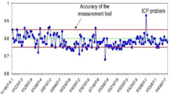
One of the most important requirements for successful application of an electro deposition technique to CIGS absorber formation is the demonstration of the ability of the technique to control the composition of the deposited films in a reliable and repeatable manner. Figure 4.2.1.a shows the Ga/(Ga+In) molar ratio data collected from the electrodeposited layers by ICP measurements during a period of 95 days. The target in this experiment was a molar ratio of 0.3 in the deposited film. The electrolyte and the process conditions were kept unchanged during the whole test period.
48
capability to include Ga in the deposited films in a reliable and repeatable manner. Figure 4.2.1.b shows the Cu/(Ga+In) molar ratio data collected from the same plated samples during the same 95-day period. The target ratio in this case was 0.8, and as can be seen from the data, this ratio was controlled between the values of 0.76 and 0.84 as measured by ICP. This is within the accuracy band of the measurement method, and therefore the results demonstrate a good ability for the technique to control composition. It should be noted that for the two excursion points in the data of Figure 4.2.1.b, the measurement instrument was found to be faulty. The data of Figures 4.2.1.a and 4.2.1.b were collected from the batch process line to evaluate the behavior and stability of the plating baths. As the above results demonstrated, even for baths with limited volume, the chemistry did not show any time-dependent instabilities.
Figure 4.2.1.a. The Ga/(Ga+In) molar ratio data collected from samples electroplated during a period of 95 days. Experiment was
carried out in the batch plater.
Figure 4.2.1.b. The Cu/(Ga+In) molar ratio data collected from samples electroplated
during a period of 95 days.
In addition to the repeatability and robustness of the electro deposition process in terms of its compositional control, experiments were also carried out with the roll-to-roll electroplating tool to demonstrate that the film thickness and the stoichiometry were uniform throughout a large-area substrate. In one early experiment during the Phase I program, a 13.5-in.-wide and 400-ft-long foil substrate was continuously processed through the roll-to-roll electroplating system and then the deposited film thickness, the Cu/(Ga+In) ratio, and the Ga/(Ga+In) molar ratio were measured across the 12.5-in.-wide section of the web as well as along the web, at 100-ft intervals. The thickness of the deposit was found to be within 10% of the target value.
Figure 4.2.1 c Back-contact resistivity for different types of contacts and the stability
49
ADVANTAGES:
The system generates plasma between a pair of rollers connected to power supply. Since the surface of the rollers is covered with the film substrate to be coated, the system does not have powered electrodes to be contaminated with the coating, and this results in stable process during a long deposition process for a web.By using HMDSO/O2 mixture as process gases, the
system is able to deposit SiOx coating as a deposition rate up to 900nm·m/min.
This mechanism gives the following advantages
High material use efficiency High deposition rate
Low contamination
7.6 CONCLUSION
From the investigation of CIGS production, test shows that the solar cells efficiency increases with increase in the source temperature, and roll to roll electroplating process is the low cost method for the production of the CIGS layer in the thin film production process. The deposition rate of the material is uniform in this process and the contamination in the production is very low when compared to other methods. Thus electroplating had given more advantages when compared with the other methods.
REFERENCES
1.Akimoto, K., Ishizuka, S., Yanagita, M., Nawa, Y.,
Goutam K. P. & Sakurai, T. (2006). Thin film deposition
of Cu2O and application for solar cells. Sol. Energy,
Vol. 80, 715-722
2.Anandan, S., Wen, X. & Yang, S. (2005). Room
temperature growth of CuO nanorod arrays on copper
and their application as a cathode in dye-sensitized solar
cells. Mater. Chem. Phys., Vol. 93, 35-40
3. V. S. Arunachalam (Center for Study of Science,
India) and E. L. Fleischer
(MRS) MRS Bulletin (2008).
4. M.A. Contreras, K. Ramanathan, J. AbuShama, F.
Hasoon, D.L. Young, B. Egaas and R. Noufi, Prog.
Photovolt: Res. Appl. 2005; 13:209–216.
5.M. Contreras, M. Romero, B. To, F. Hasoon, R. Noufi,
S. Ward and K. Ramanathan, “Optimization of CBD
CdS Process in High-Efficiency Cu(In,Ga)Se2-Based
Solar Cells,” Thin Solid Films, Vol. 403-404, No. 579,
2002, pp. 204-211.
6. A. Davis, K. Vaccaro, H. Dauplaise, W. Waters and J.
Lorenzo, “Optimization of Chemical Bath-Deposited
Cadmium Sulfide on InP Using a Novel Sulfur
Pretreat-ment,” Journal of The Electrochemical Society, Vol.
146, No. 3, 1999, pp. 1046-1053.
7.Fortin, E. & Masson, D. (1981). Photovoltaci effects in
Cu2O-Cu cells growing by anodic oxidation. Solid-St.
Electron., Vol. 25, 4, 281-283
8.Garuthara, R. & Siripala, W. (2006).
Photoluminescence characterization of polycrystalline
n-type Cu2O films. J. Luminescence, Vol. 121, 173-178
9. Ghijsen, J., Tjeng, L.H., Elp, J. V., H. Eskes,
Westerink, J., & Sawatzky, G.A. (1988). Electronic
structure of Cu2O and CuO. Phys. Rev., Vol. 38,
11322-11330
10. Guy, A. C. (1972). Introduction to Material Science
(International Student Edition), McGraw-Hill, Tokyo