Continuum Computing – on a New Performance Trajectory
beyond Exascale
Thomas Sterling1, Maciej Brodowicz1, Matthew Anderson1 c
The Authors 2018. This paper is published with open access at SuperFri.org
The end of Moore’s Law is a clich´e that none the less is a hard barrier to future scaling of high performance computing systems. A factor of about 4×in device density is all that is left of this form of improved throughput with a 5×gain required just to get to the milestone of exascale. The remaining sources of performance improvement are better delivered efficiency of more than 10×and alternative architectures to make better use of chip real estate. This paper will discuss the set of principles guiding a potential future of non-von Neumann architectures as adopted by the experimental class of Continuum Computer Architecture (CCA). It is being explored by the Semantic Memory Architecture Research Team (SMART) at Indiana University. CCA comprises a homogeneous aggregation of cellular components (function cells) which are orders of magnitude smaller than lightweight cores and individually is unable to accomplish a computation but in combination can do so with extreme cost efficiency and unprecedented scalability. It will be seen that a path exists based on such unconventional methods like neuromorphic computing or dataflow that not only will meet the likely exascale milestone in the same time with much better power, cost, and size but also will set a new performance trajectory leading to Zettaflops capability before 2030. The remainder of this paper is organized as follows. Section 1 describes a new class of high performance architectures and discusses the rationale for its introduction. The scaling analysis is presented in section 2. Future performance projections, including steps leading to Zettaflops, are outlined in section 3. Finally, the principal outcomes of this study are summarized in the conclusions section.
Keywords: high performance computing, parallel computing, exascale, non-von Neumann ar-chitecture.
Introduction
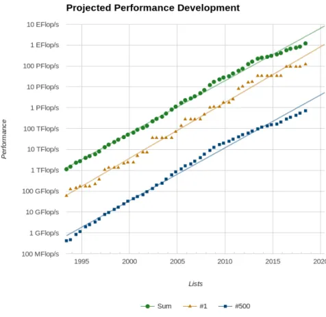
The fastest computer in the world measured by the HPL or Linpack benchmark [5] is the Summit [19], at Oak Ridge National Laboratory, in the United States. As recently measured, its performance is 188 Petaflops peak performance and 122 Petaflops Rmax. Number 1 on the June
2018 Top-500 List [2], it is followed by two Chinese systems with TaihuLight coming in at Number 2 and 93 Petaflops Rmax positioned there for two and a half years. Following these are 498
HPC systems with the 500th still measured in the hundreds of Teraflops. These unprecedented advances reflect an exponential progress over a period of more than two dozen years with a total growth of more than a factor of a million over that period and of more than ten trillion since the beginning of the age of the modern digital electronic stored program computer more than 70 years ago. Much of this is a combination of von Neumann architecture [17] derivatives and the sustained improvement of device components often regarded as Moore’s Law [16]. The current era could perhaps be referred to as Pax Semiconductor as the constant tick-tock of produce development and delivery has provided the confidence of continued improvements into the indefinite future. However, as the enabling technology approaches that of nano-scale measured in number of atoms of thickness, the previous trends that have gained us so much are meeting their terminus. Feature sizes, power consumption, and clock rates are all reaching their flat asymptotes while parallelism both at ILP and concurrent processes are struggling to grow. Even as HPC capabilities approach exascale, admittedly at enormous cost, the future embracing passed conventional practices is uncertain and of questionable utility.
Although the age of digital computing exhibits the semblance of a continuity of performance growth and therefore the appearance of sameness, the truth is far more complex. There have been at least six phases of computing paradigms to exploit the evolving capabilities of enabling tech-nologies. In each case, both computer architectures and programming models with supporting software have changed distinctly in response to driving technology advances to take advantage of their opportunities and to address the challenges they impose. One possible delineation of these epochs with very fuzzy overlapping borders is presented as:
I. Genesis – vacuum tubes, magnetic storage, von Neumann architecture (e.g., EDSAC, UNIVAC).
II. Transistor – semiconductor, micro-control, operating system (e.g., IBM 7090, CDC 6800).
III. SSI (small scale integration) – first generation integrated circuits (e.g., DEC PDP-8, IBM 360).
IV. MSI (medium scale integration) – vector pipeline FPU, vector register (e.g., Cray-1).
V. LSI (large scale integration) – SIMD (e.g., TMC CM-2, MASPAR-1).
VI. VLSI (very large scale integration) – MPP, commodity clusters, networks (e.g., Beowulf, Intel Touchstone Delta, Cray T3E, Red Storm).
VII. Multi-core – multiple processors per socket (e.g., IBM Roadrunner, Sunway TaihuLight).
VIII. Heterogeneous – integrated specialized computing components (e.g., IBM/NVIDIA Sum-mit).
As indicated, each of these epochs comprise a distinction in form and function in response to technology. With the new challenges of the end of Moore’s Law, it is important to determine the next set of innovations that will force future computing methods and means if HPC is to extend beyond the boundaries of exascale by the beginning of the next decade. Even now forwarding looking concepts are being researched within academia and industry in areas such as quantum computing and neuromorphic computing. Quantum Computing directly exploits quantum me-chanical phenomena to store the equivalent of many bit values in a single storage element called a “qubit” [20] and process the many possible solutions at the same time, delivering one of the results at the end. Cooled to a fraction of a Kelvin these devices employ quantum superposition and entanglement to achieve this. For some algorithms, exponential scaling should in principle be achievable with polynomial scaling for others. It is recognized that a conventional computer would take longer than the lifetime of the universe (i.e., 13.82 billion years) to accomplish what a future quantum computer may be able to do in finite time.
both quantum computing and neuromorphic computing are, much work in both methods will be required. But the challenges facing the future of computing are immediate and alternative techniques are required.
The remainder of this paper discusses an alternative conceptual strategy based on near-term semiconductor technologies but, perhaps more than in previous epochs, embracing innovations in computing model, architecture, and programming. Like all previous generation systems this addresses the fundamental factors that determine ultimate performance. These are: starvation, latency, overhead, and contention with additional concerns of energy consumption and reliabil-ity. But it relaxes the constraints inherent to essentially all previous widely used HPC systems. Specifically, it employs dynamic adaptive parallel task scheduling and resource management as opposed to conventional static system and application management. Of equal or more sig-nificance, is the abrogation of premises implicit in all von Neumann derivative architectures (exclusively populating the Top 500 list [1]: Fig. 1) to liberate computer architecture from the constraints of legacy machines and opening up new possibilities through potential non-von Neu-mann architecture, still within the realm of known enabling technologies and chip fabrication methods and facilities. The conclusion of this paper as will be shown is that far from being in-carcerated in performance by the end of Moore’s Law, opening a new path to non-von Neumann yields new opportunities to future performance growth. Early analysis suggests more than three orders of magnitude peak performance in less than a decade.
1. Foundation Concepts for CCA
HPC applications are expanding to encompass not just conventional static numeric inten-sive problems but also those incorporating complex data structures typified by time-varying and irregular organizations referred to generally as dynamic graphs. Rapidly expanding market domains such as data analytics, machine learning, facial and voice recognition, autonomous ve-hicles, crypto-currency, the internet of things (also referred to as sensor nets), and 3-D virtual reality, are among other new computational application targets. There are a number of competi-tive approaches to satisfying user demands related to these and other scientific and commercially valuable problems including conventional multi-core SMP and MPP configurations and hetero-geneous system architectures mixing general purpose processors with GPU accelerators. For some user applications, these types of systems are effective. But two major challenges are facing the future of fast computing and in so doing are opening new opportunities that, with insightful innovations, may be satisfied exposing the potential for new system classes and capabilities. These are the limited future scalability due to the end of Moore’s Law and constrained power and the computing data access patterns with minimal data reuse. The proposed innovations present the opportunity for a new class of computing that address these and other challenges while exploiting largely untapped improvements. These are described in detail here.
It is ironic that the single most dramatic technology in terms of rate of growth is also very conservative. Over more than six decades, in spite of the multiple transitions in enabling tech-nologies from vacuum tubes to multi-core sockets, the von Neumann architecture has dominated with the apparently diverse computing classes (e.g., vector versus communicating sequential processes (CSP) [9]) almost all von Neumann derivatives. The trade-offs implicit to the von Neumann architecture, once entirely justified, are no longer optimal; possibly the opposite as related to todays enabling technology. One of the staples of computing has been the compiler de-termined static management of resources and task scheduling. This traditional method has been effective for regular static algorithms. But for those many problems with behavior determined by intermediate results, runtime information is required to guide both task scheduling and re-source management, especially for distributed systems with large memory hierarchies and widely varying latencies of access. The challenges of starvation, latency, overhead, and contention for shared resources must be addressed by any computing system. The proposed innovations provide innovative techniques for doing so.
The proposed strategy combines an innovative non-von Neumann architecture to employ current and future enabling semiconductor technologies with a control methodology based on the ParalleX execution model [6, 11] for dynamic adaptive resource management and task scheduling to deliver superior efficiency and scalability. Together they address their mutual needs in synergy to provide potential customers with low cost solutions to their computing requirements. These are described in detail below with the resulting value delivered following.
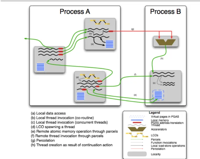
1.1. ParalleX Dynamic Control
Figure 2. Components of the ParalleX execution model
fine grain parallelism for scalability, and latency hiding. The hardware architecture delivers all of these mechanisms to the performance of the ParalleX execution model.
ParalleX replaces the CSP execution model that has served and dominated large scale HPC for the last three decades providing a new dynamic methodology in place of the old static techniques. ParalleX integrates four key properties to enable dynamic adaptive execution, greater scalability through exposing and exploiting greater parallelism, and addressing as well as exploiting asynchrony of execution. These key constructs are:
• Global address space that enhances user productivity and performance portability.
• Local dataflow parallel tasks.
• Message-driven computation.
• Asynchronous Futures/dataflow synchronization constructs.
And, it overlaps successive phases of computation by avoiding global barrier synchronization for more effective parallelism. Latency is another source of performance degradation and ParalleX delivers methods of mitigating both latency and the asynchrony to which it contributes. As pre-viously identified, ParalleX supports lightweight thread context switching for non-blocking and overlaps computation and communication to hide latency to limit its effects. It employs massage-driven computation to move the work to the data rather than always moving the data to the work thus reducing actual latency under some conditions through the reduction of number and size of global messages. Perhaps the most insidious of the SLOWER factors is overhead work. It not only imposes useless work adding time to the computation and energy consumption as well. But for a fixed amount of work (strong scaling) it establishes an upper bound on the total performance achievable independent of the quantity of hardware dedicated to it. ParalleX-based systems achieve this by mostly eliminating global barriers, employing synchronization objects exhibiting high semantic power with respect to amount of work required. It reduces context switching time. And for specific actions, thread instantiation is not required thus avoiding its overheads completely in the case of very lightweight tasks that are most sensitive to overheads. Finally, contention is a source of bottlenecks most recognized in the forms of memory access bandwidth and network bandwidth. Ironically, it is ALU limitations that are the source of largely unacknowledged contention that is addressed in brute force fashion through scaling. ParalleX class systems approach this through adaptive resource allocation with a multiplicity of resources and by eliminating polling. It also facilitates adaptive routing to work around hot spots.
Multiple early implementations of the ParalleX execution model have been developed in the form of runtime systems software in support of applications that will benefit from these capabilities such as adaptive mesh refinement, fast multipole methods, particle in cell codes, and deep learning. But limitations in efficiency were measured due to overheads of key mechanisms for some applications more suitable to conventional practices. Nonetheless, the ParalleX model was demonstrated as an effective abstraction for capturing and controlling the interface between parallel applications and parallel architectures such as the non-von Neumann one here.
An implementation of the ParalleX execution model was the HPX-5 runtime system software package and employed for a wide range of applications. Among the many measurements taken of the SLOWER performance factors were the major ways in which overheads intruded into the overall operation of the parallel system. This work was performed by Daniel Kogler, a graduate student at Indiana University, exposed a surprising result. It was shown that while the minimum of overhead times was in the hundreds of nanoseconds, there was a very wide distribution of times; as much as a factor of two in some cases and approaching an order of magnitude in others. This variability which was unexpected creates a new problem and is caused by as well contributes to the uncertainty of asynchrony.
longest main memory blocks across the extent of the distributed system. The sensitivity is not just with the inherent distances involved but to data placement and localities, both temporal and spatial. Another source of asynchronous behavior is due to scheduling conflicts for shared resources by multiple concurrent threads. The order of scheduling is undetermined in part due to other asynchronies therefore increasing the variability of tasks, but time to initiation and time to completion. To manage power consumption based on resource control, systems will actively and sometimes automatically vary voltage and clock rates causing variability of time for operations to be performed, adding to the asynchrony. Other sources also exist that extend the uncertainties of asynchrony even more. Therefore, systems need to be designed that are able to respond and adjust to asynchronous operation and where possible reduce both the times and variability of actions. One important implication is that new hardware mechanisms be incorporated in future architectures to mitigate these overheads and their uncertainty. Processor core architecture that includes such mechanisms to support parallel processing overheads for this purpose is discussed in section 1.3.
1.2. The von Neumann Cul-de-Sac
Figure 3.John von Neumann (left) and Robert Oppenheimer (right) in front of the IAS computer
share. As a result, complicated core designs emerged with many layers of memory hierarchy (caches) transparent to the user, speculative execution such as branch prediction and memory access, associative mechanisms such as TLBs and cache line selection, and a plethora of other specialized functions to incrementally extend the capabilities just a bit farther than the previous tick-tock product cycle. As all these specializations accrued, the relative size, cost, and power of the ALU itself became minor in comparison. The other major change was that of the enabling technologies themselves and their interrelationships. Initially, major classes of components (i.e., memory, logic and control, and communication) were distinct (e.g., vacuum tube logic versus magnetic core memory) and by their intrinsic nature were physically separated. But now and for many years all three of these component categories are realized in semiconductor technology. In principle, they need not be divided, but due to legacy of the von Neumann model, are forced to be so to this day.
As a result, there are a number of inherent underlying assumptions intrinsic to commer-cial computing systems derived from the von Neumann model that forces poor design choices compared to what would be possible with contemporary semiconductor technologies through architecture structures and control semantics if not constrained by von Neumann precepts. A few but not all of these can be identified as the following:
1. FPU utilization is still prescribed as primary metric of efficiency dictated by von Neumann when the FPU is now a very small part of the core die area and power consumption. Yet the majority remaining area of the core architecture serves little other purpose than to keep the FPU busy; clearly a false objective function.
2. The processor core logic including the FPU and the main memory of the computing system are historically separated on different integrated circuits with intervening communication paths, constraining data access bandwidths, imposing significant data access latencies, in-creasing energy costs of data access, and demanding substantial interface and control logic for memory access. This is known as the “von Neumann bottleneck.” With both logic and main memory both implemented with semiconductor technology, in principle the logic and memory could be mutually integrated on the same die largely eliminating these degradation factors.
3. To maintain the above requirement of running the ALU at fastest rate which is two orders of magnitude greater than DRAM, layers of cache memory taking up space and power are interposed based on the hope of temporal and spatial locality. As the caches are transparent to the user, this is supposed to make it easier to use. Ironically, for HPC the obvious is the case as the cache operation policies conflict with the needs of the user; yet, the user cannot control the cache.
required to keep the potentially many copies of a data set to retain synchrony with costs in time, die space, and energy.
6. To further retain the appearance of sequential execution even with parallel operations, in-struction level parallelism (ILP), execution pipelining, reservation stations, and speculative execution such as branch prediction all require additional and sometimes substantial mech-anism hardware (and compiler instruction ordering software) to deal with these as well as pipeline hazard resolution. Die area, time, and energy are all sacrificed to a degree to assert von Neumann dictates.
7. Registers were an early addition and extension of the original von Neumann buffers to in-crease bandwidth and reduce latency to logic and are a mainstay of todays processor cores with both large sets of registers and sometimes multiple such sets. The registers are inde-pendent of the main memory and enforce a load/store protocol. Registers are so intuitively obvious that they are never questioned (except in GPU accelerators) and their presence assumed. Nonetheless, they are an additional cost in terms of the usual metrics.
8. Virtual address TLBs and page tables are a means to exhibit a uniform memory image required by the von Neumann model but across the complex main memory and secondary storage hierarchy. This method has never been sufficiently mastered in terms of time effec-tiveness but nonetheless is required with substantial costs in hardware mechanisms (not to mention OS services).
As a result of the above constraints and costs imposed by the von Neumann model and the now rapidly approaching end of Moore’s Law and clock rates, future performance growth is most likely only achievable to any great degree through innovations of computer architecture. The often-successful use of GPU accelerators demonstrates one possible approach by augment-ing conventional architectures with special purpose devices in a generalized approach referred to as heterogeneous computing. Where a particularly important algorithm with commercial market value can be accelerated through special purpose architectures such as the D.E. Shaw Anton architecture [21] optimized for molecular dynamics simulation. Here we propose a new non-von Neumann architecture that is more general than SPDs, addresses new market niches in graph processing, data analytics, machine learning, and other domains. The proposed archi-tecture is based on its value to these customer problem domains by exploiting the described and fundamental disadvantages of the von Neumann architecture through an innovative class of physical structures combined with a dynamic adaptive strategy of parallel computing based on the ParalleX model. It is upon this significant innovation that we are launching our new business enterprise.
1.3. Continuum Computer non-von Neumann Architecture
equiv-alents) and the design of a global simple structure of replicated cells. This novel approach with respect to conventional practices makes the objectives of this project feasible within the scope of resources and period of performance. The global structure is as simple as adjacent connectivity to neighboring cells which is straight forward. To extend the system to multiple chip sockets again is accomplished through nearest neighbor socket to socket interconnects. Beyond Phase 1, a last level of interconnect between nearest neighbor PC boards will provide total design capacity of data storage active memory capacity and peak operational capability. The investigators are considering a second hierarchical network spanning the global system emphasizing low-latency lightweight messaging but for the active memory accelerator, prescribed target market, and cus-tomer segment this extensibility will be unnecessary and beyond the scope of the proposed work and product offering.
Continuum computer architecture based on the active memory system will engage ancillary functionality for support activities. Such services include bootstrapping, user program loading, host to accelerator I/O (in this case with PCI-Express), configuration on-board switches and output lights, and JTAG. These features will be supported by an FPGA controller, also to be designed, and integrated on the same PCB as the cell array chips. Not only does this controller provide flexibility in accelerator design, it permits debugging and upgrades of end user products. The FPGA controller is supported by an adjacent SRAM for available scratchpad memory and Flash NVRAM for FPGA controller internal configuration and system initialization. Associated with each cell array socket is a DRAM chip of service memory which is not part of the global virtual address space nor part of the user memory but rather dedicated local storage for copies of codes, tables, lightweight operating system support, overflow from active memory, and other secondary purposes. This service memory can be accessed by any cell on the specific socket.
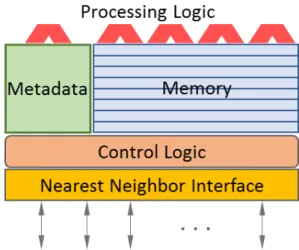
Figure 4. Generalized CCA cell architecture
Critical among these is the bandwidth and latency between the active memory and logic which are essentially the same component. The data path is not word wide but line width to permit operations on multiple fields simultaneously. There are no separate registers but rather the block of multiple active memory lines. The technology used for active storage is a variation of SRAM not unlike that employed for level-2 caches. However, each block line includes some internal logic for primitive operations that can be performed in parallel. Examples include shift and roll operations, increment/decrement over masked ranges, GF-2 [12] for government customers, associative searches, and necessary primitives for dynamic graph processing.
Figure 5. Example tessellation of silicon die area implementing cell array
The second class of functionality integrated in the computing cell is the combination of addressing and routing for virtual address management and data transfers. This is particularly important for rapid pointer tracing for parallel graph processing which discovers and exploits meta-data parallelism. Communication is primarily nearest neighbor. The cell to be designed is triangular (Fig. 5) for simplicity and to minimize hardware communication overhead with respect to storage and logic. It also provides very tight packing on the silicon die. But several other geometries are possible as well with different trade-offs.
model. Again, contiguous assemblies of cells with instructions interspersed with data provide locality, atomic operation sequences, and open-ended flexibility of functionality. Such structures also permit graph tracing.
1.4. Graceful Degradation
The ability to achieve fault tolerance, that is non-stop computing, is challenging and com-plicated, rarely achieved, with the fall back of venerable checkpoint-restart often applied for large scale systems and applications. For special purpose cases such as systems control (e.g., flight control), a multiplicity of systems running the same codes are employed concurrently to continue operation even in the presence of one failing providing both error detection and contin-ued operation. But this is an expensive brute force approach aggravating cost, power, size, and weight. The proposed target market, that of crypto-currency, suffers from failures that result in potentially significant profit reductions due to periodic down times of forced maintenance with the need for the replacement of component modules prior to operation again.
Full fault tolerance would require a number of steps available and automatically performed by the hardware software system. These include error detection, failure diagnosis, replacement of component, roll back of computation to known good point, restart. Slightly different methodolo-gies are also employed. But for some computations and systems such as the one being proposed a simpler and less costly methodology is sufficient for the customer purposes. Graceful degrada-tion (not a new concept) incorporates means by which a systems capabilities diminish over time with incurred hardware faults but continues to operate, albeit at reduced performance. Such techniques can be made more complex due to the need to safely restart a partially completed task. However, in the case where a myriad of disconnected tasks is being performed such as transaction systems (e.g., a Google query), the task associated with the failed device can be dropped, simplifying the recovery.
1.5. Detailed Value Achieved through Innovations
Many advantages are achieved through the innovative non-von Neumann architecture de-scribed above with additional ones not yet discussed. Here is summarized many of the specific values garnered through this unique structure and semantics:
• Reliability is achieved through turning off cells that are defective and using adaptive rout-ing to work around these holes. Graceful degradation avoids many srout-ingle point failure modes dramatically reducing or even eliminating the need for checkpoint-restart over-heads.
• Higher yield to lower cost of chip manufacturer by up to 2× which also reduces testing cost for 1.5×customer price reduction. This results from the same value above where the random faults encountered in die fabrication are simply cut off from the rest of the chip and adaptively routed around. This will make almost all dies of the wafer usable, thus reducing cost of production and price to customer.
• Increase of computational throughput normalized by size compared to conventional prac-tices by 100×, at least peak performance, results from the elimination of most of the core die area of typical chips allowing far greater logic density and resulting number of cells served by much greater memory bandwidth.
• Enabling asynchronous graph processing with built in synchronization, futures in vertices.
• Enabling scalable parallel graph processing with hardware support for direct manipulation of meta-data (pointer type) to discover, expose, and exploit parallelism and convert serial issue to parallel (logarithmic) issue from source vertex to many destination vertices.
• Eliminate distance barrier between data storage (formerly main memory) and data trans-formation (formerly separated ALU/FPU logic) by merging the two (PIM [7] is another variant) to minimize latency between state and logic (von Neumann bottleneck).
• Power reduction of 95% normalized to throughput.
• Active memory replaces main memory, scratch pad memory, caches, and registers. Simpli-fied programming model and greater portability.
• ALUs emphasize availability, not utilization. Greatly enhances overall efficiency and pro-grammability.
• Maximize local active memory bandwidth through merger of logic and storage as well as wide word (struct) processing. Lower power, faster processing, greater efficiency. Customer applications good even with low data reuse enabling to do different types of science that were less well suited to conventional methods.
• Maximize local bandwidth through nearest neighbor direct point to point adjacency in-terconnect and between sockets to lower communication power and increases efficiency for problems like using stencils.
• ParalleX dynamic adaptive execution model for scalability and simplification of program-ming.
• Global address space.
• Message driven computation.
• Futures synchronization.
• Locality management.
2. Scaling Opportunities derived from CCA Class Systems
2.1. CCA as a non von Neumann Strategy
The true importance of the opportunities delivered by the CCA class of non-von Neumann systems is in the dual properties of efficiency and scalability. At one time, it was conventional practice to measure efficiency in terms of FPU utilization; that is the ratio of sustained floating-point performance to peak performance. This had been extended to use the HPL benchmark as the metric of the sustained performance. This was a favorable parameter to industry vendors of large scale systems whose designs optimized their core and system architectures to local floating-point operations. But other measures of efficiency are far more important as enabling technologies follow current trends. These emphasize different objective functions; among these: cost, energy, availability, and size. The ParalleX model was based on the intent to use runtime information and control to make better use of resources, thus exhibiting superior efficiency than compiler-driven methods alone. It was seen to achieve this in certain cases such as computations that embrace dynamic adaptive methods such as adaptive mesh refinement or finite multiple methods. But in other cases, static methods proved to be adequate, even superior depending on details of the runtime implementation. Key to enhancing effectiveness of runtime techniques was the reduction or elimination of parallel control overheads through hardware mechanisms. New architectures, including CCA, expose such opportunities. More broadly, for a given problem efficiency is a function of the time to solution and the cost including deployment and operational. Within this cost is energy. What becomes clear is that utilization is not a direct indicator of efficiency. Heterogeneous computing alternatives exploit this fact where overall utilization may be lower but time to solution is also shorter.
2.2. Principles of CCA Scaling
expands availability and reliability. Fourth, system bandwidth dramatically grows with every cell having immediate access to state of its adjacent neighboring computing cells. Fifth, energy is reduced as only those cells undertaking constructive work during any single system cycle has to consume energy; this could be considered a form of active dark silicon. Sixth, there is a marked change to the creation of such system from the common practice of achieving complexity of operation through complexity of design of processor cores to the alternative of achieving complexity of operation through simplicity of design of computing cells and their high replication. A consequence is that a computing cell can be developed by a small group of engineers in a small amount of time and cost less for the NRE. It is these and other properties that determine the nature and value of the class of “continuum computer architecture.”
2.3. CCA Scaling Analysis
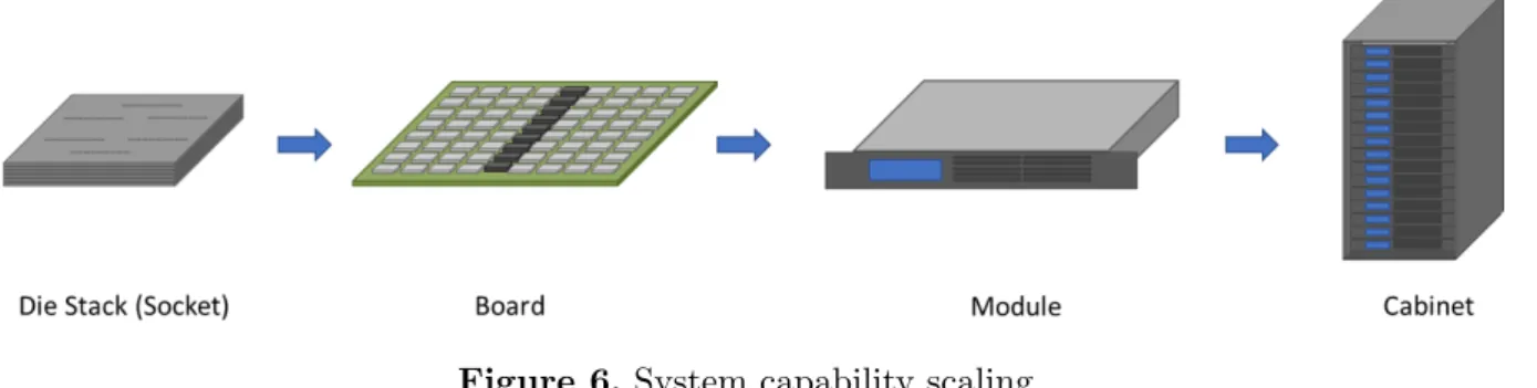
The details of the internal design of a computing cell are not presented in this paper. There are many possible solutions and their variations to this problem and will be the subject of future disclosure and discussion. But such specifics are not needed to explore the remarkable poten-tial scalability of CCA systems even within the scope of conventional semiconductor enabling technologies and their immediate extensions in the nano-scale regime. The following analysis does not presume any inherent breakthroughs than those already discussed which is largely a change of perspective and frankly a willingness to consider a design space beyond that of legacy approaches. Ironically, once the transformative principles of CCA are embraced, the scalability of systems that are so derived is essentially one of incrementalism. This is illustrative in the typical form of a hierarchy of system components from individual computing cells, chips con-taining on the order of 10,000 such cells, one or more such chips in a socket, a multiplicity of sockets on a 16” by 10” PC board, one to four boards to a module. For sake of clarity and as determined from design studies, the range of modules structures can all fit within a 1-U rack mounted package using air-cooled with one to two boards and liquid cooling for three to four boards. The module can be used as an attached accelerator to a conventional user SMP system or as one of a plethora of units interconnected by a system area network (Fig. 6).
Figure 6.System capability scaling
Using available technologies from which to construct nodes, part densities, capabilities, and power are determined. It is estimated that a computing cell as described in previous sections will comprise 100 to 200 thousand transistors.
Table 1. System component counts
Level Cells Chips Sockets Boards Modules
Chip 11 k 1 - -
-Socket 43.8 k 4 1 -
-Board 16.3 M 1,488 372 1 -Module 65.2 M 5,952 1,488 4 1 Rack 2.74 G 250 k 62.5 k 168 42 System 65.7 G 6 M 1.5 M 4,032 1,008
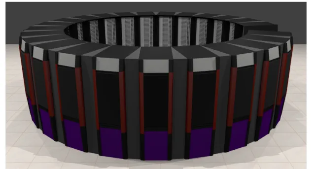
milestone is the module of 1 Petaflops of peak performance (liquid cooled) from which many different configurations are possible in scale both as active memory accelerators and as full self-hosted standalone supercomputers. A rendering of an Exaflops computer is shown in Fig. 7 1 as a cylindrical configuration of conventional industrial grade racks. An important metric is footprint for any supercomputer. This system, using only available enabling technologies, requires less than 400 square feet which is almost two orders of magnitude smaller than using common practices. Although of small interest, for practical reasons weight is another consideration. A fully populated rack comes in just under the industry standard limits of 1,200 Kilograms in a foot print of less than 1 square meter. The total Exaflops system is about 30,000 Kilograms.
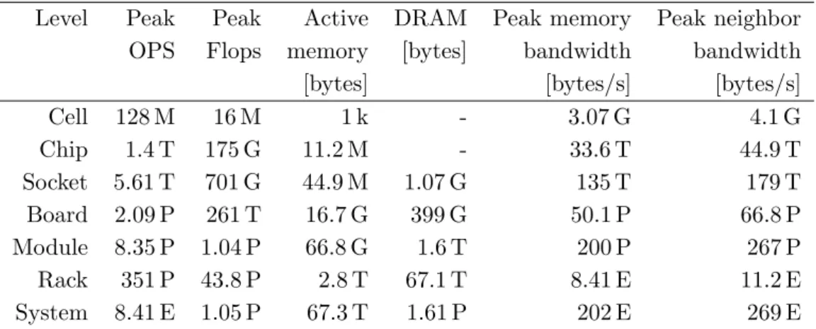
Table 2.Capacities of system components
Level Peak Peak Active DRAM Peak memory Peak neighbor OPS Flops memory [bytes] bandwidth bandwidth [bytes] [bytes/s] [bytes/s] Cell 128 M 16 M 1 k - 3.07 G 4.1 G Chip 1.4 T 175 G 11.2 M - 33.6 T 44.9 T Socket 5.61 T 701 G 44.9 M 1.07 G 135 T 179 T Board 2.09 P 261 T 16.7 G 399 G 50.1 P 66.8 P Module 8.35 P 1.04 P 66.8 G 1.6 T 200 P 267 P Rack 351 P 43.8 P 2.8 T 67.1 T 8.41 E 11.2 E System 8.41 E 1.05 P 67.3 T 1.61 P 202 E 269 E
2.4. Power Consumption
Figure 7. Rendering of an Exaflops system composed of 24 racks in a circular arrangement. A rack-wide opening is left for maintenance access to the back of cabinets
into account the die count in the Petaflops module and additional power requirements of the system level interconnect, module’s power draw is estimated at 7.2 kW, fully populated rack’s at 316 kW, and the exascale system at 7.6 MW.
3. Scaling to Zettaflops
With the advent of the venerable (by computer years) TaihuLight and the genesis of the Summit 200 Petaflops system, it is anticipated that extensions of current methodologies will empower the eventual deployment of exascale computing by the beginning of the next decade. There is a major international thrust by many countries to do just that. With the will to invest hundreds of millions of dollars, large machine rooms, and large power consumption, the exascale era is upon us. Adopting an entirely new form and function of computing concept, even if superior by key metrics, is probably unjustifiable if it were targeted to this singular operating point. But such is not the case. A set of incremental advances is identified that in some, as yet to be identified order, can traverse the pan-exascale performance regime. It appears this can be accomplished in less than a decade with full deployment of Zettaflops scale systems delivered on or before 2027. The following is a brief description of these possible steps beyond the analysis for 1 Exaflops CCA.
1. Switching from a circular foot-pad to the conventional rows of racks and doubling in both length and width will yield a 4×peak gain.
2. The original clock rate used for all analysis was 128 MegaHertz. It is planned that in incre-mental steps of doubling that the final clock rate will be the modest 500 MHz for another 4×is peak speed.
4. Over the span up to 2027 and perhaps significantly before, the path to nanoscale (and sadly the end of Moore’s Law) will likely permit feature sizes to move from 16 nm which the original exascale analysis used to 8 nm which is already working in the laboratories of semiconductor manufacturers. This provides a doubling of density in chip length and width for a 4×gain in number of computing cells per die and peak performance gain.
5. ILP (instruction level parallelism) was ignored for the original analysis assuming that a computing cell either does nothing during a particular cycle or does one action. But the local structure permits many micro-operations per cycle and a conservative estimate of performance advantage through responsible ILP will deliver at least a 4×peak performance gain.
6. An assumed 1 cm2 die size was employed throughout the exascale CCA analysis in the preceding sections. But this is limiting. The die even in todays technology could be twice the size in each dimension for a 2 cm by 2 cm die. This does not increase the cell density. But it does have a secondary effect of improving the PC board area utilization by 50% resulting in a 1.5×performance increase.
7. The last technique to extend system capability is to break with one of the long-held as-sumptions about digital computing, that its hardware is base-2. In fact, Boolean logic is not restricted to base-2 and it is possible to build circuits in memory and logic to work at base-4 (and above). It is recognized that this is a radical departure from the norm. But it is entirely feasible saving space, time, and energy. It is included here to achieve one last doubling for another 2×of peak performance.
In each case, the factors of gain reflect various degrees of risk from trivial and obvious to more speculative. But these seven dimensions in the design space if combined and acknowledging that this is entirely in terms of peak performance will provide a roadmap to a gain of 1,500×which is equivalent to Zettaflops. This does not constitute a detailed analysis but only a framework for considering the future roadmap for CCA class systems in the next decade. But it is sufficient to have confidence in a future path.
Conclusions
This paper is an early presentation on the concept of Continuum Computer Architecture, a family of non-von Neumann architectures that relax many of the constraints and bottlenecks of conventional computers. This treatise projects the possibility of exascale computer platforms much less expensive, and lower power than extrapolations of conventional practices. The com-bination of the ParalleX execution model and the CCA is considered to enable pan-exascale performance through practical evolution in the near future. It is concluded from this study that Zettaflops computing is conceivable within the next decade.
This paper is distributed under the terms of the Creative Commons Attribution-Non Com-mercial 3.0 License which permits non-comCom-mercial use, reproduction and distribution of the work without further permission provided the original work is properly cited.
References
1. Top 500 performance development (Jun 2018), https://www.top500.org/statistics/ perfdevel/, accessed: 2018-07-17
2. Top 500. The List. (Jun 2018), https://www.top500.org/, accessed: 2018-07-17
3. ARM Holdings Architecture Group: ARMv8 Instruction Set Overview (Nov 2011), PRD03-GENC-010197
4. Black, B., et al.: Die stacking (3D) microarchitecture. In: Proceedings of the 39th An-nual IEEE/ACM International Symposium on Microarchitecture, MICRO’06. pp. 469–479 (December 2006), DOI:10.1109/MICRO.2006.18
5. Dongarra, J.: Performance of various computers using standard linear equations soft-ware. Tech Report CS-89-85, University of Tennesse Computer Science (2014), http:
//www.netlib.org/benchmark/performance.pdf, accessed: 2017-07-17
6. Gao, G.R., Sterling, T., Stevens, R., Hereld, M., Zhu, W.: Parallex: A study of a new par-allel computation model. In: 2007 IEEE International Parpar-allel and Distributed Processing Symposium. pp. 1–6 (March 2007), DOI: 10.1109/IPDPS.2007.370484
7. Hall, M., Kogge, P., Koller, J., Diniz, P., Chame, J., Draper, J., LaCoss, J., Granacki, J., Brockman, J., Srivastava, A., Athas, W., Freeh, V., Shin, J., Park, J.: Mapping irregular applications to DIVA, a PIM-based data-intensive architecture. In: Proceedings of the 1999 ACM/IEEE Conference on Supercomputing. SC ’99, ACM, New York, NY, USA (1999), DOI: 10.1145/331532.331589
8. Hisamoto, D., Lee, W.C., Kedzierski, J., Takeuchi, H., Asano, K., Kuo, C., Anderson, E., King, T.J., Bokor, J., Hu, C.: FinFET – a self-aligned double-gate MOSFET scal-able to 20 nm. IEEE Transactions on Electron Devices 47(12), 2320–2325 (Dec 2000), DOI: 10.1109/16.887014
10. Josephson, B.: Possible new effects in superconductive tunnelling. Physics Letters 1(7), 251–253 (1962), DOI: 10.1016/0031-9163(62)91369-0
11. Kaiser, H., Brodowicz, M., Sterling, T.: ParalleX an advanced parallel execution model for scaling-impaired applications. In: Parallel Processing Workshops, 2009. ICPPW ’09. International Conference on. pp. 394–401 (Sep 2009), DOI: 10.1109/ICPPW.2009.14
12. Lidl, R., Niederreiter, H.: Finite Fields. Encyclopedia of Mathematics and its Applications, Cambridge University Press, 2 edn. (1996), DOI: 10.1017/CBO9780511525926
13. Likharev, K.K., Semenov, V.K.: RSFQ logic/memory family: a new Josephson-junction technology for sub-terahertz-clock-frequency digital systems. IEEE Transactions on Applied Superconductivity 1(1), 3–28 (March 1991), DOI: 10.1109/77.80745
14. Modha, D.S.: Brain-inspired computing. In: 2015 International Conference on Parallel Ar-chitecture and Compilation (PACT). pp. 253–253 (Oct 2015), DOI: 10.1109/PACT.2015.49
15. Monroe, D.: Neuromorphic computing gets ready for the (really) big time. Comm. ACM 57(6), 13–15 (Jun 2014), DOI: 10.1145/2601069
16. Moore, G.E.: Cramming more components onto integrated circuits. Electronics pp. 33–35 (Apr 1965), DOI: 10.1109/N-SSC.2006.4785860
17. von Neumann, J.: First draft of a report on the EDVAC. Tech. rep., Moore School of Electrical Engineering, University of Pennsylvania (Jun 1945)
18. von Neumann, J., Taub, A.W., Taub, A.H.: The Collected Works of John von Neumann: 6-Volume Set. Reader’s Digest Young Families (1963)
19. Oak Ridge National Laboratory: Summit: America’s newest and smartest supercomputer (2018), https://www.olcf.ornl.gov/summit/, accessed: 2018-07-17
20. Schumacher, B.: Quantum coding. PhysRevA 51, 2738–2747 (Apr 1995), DOI: 10.1103/PhysRevA.51.2738
21. Shaw, D.E., Deneroff, M.M., Dror, R.O., Kuskin, J.S., Larson, R.H., Salmon, J.K., Young, C., Batson, B., Bowers, K.J., Chao, J.C., Eastwood, M.P., Gagliardo, J., Grossman, J.P., Ho, C.R., Ierardi, D.J., Kolossv´ary, I., Klepeis, J.L., Layman, T., McLeavey, C., Moraes, M.A., Mueller, R., Priest, E.C., Shan, Y., Spengler, J., Theobald, M., Towles, B., Wang, S.C.: Anton, a special-purpose machine for molecular dynamics simulation. Commun. ACM 51(7), 91–97 (Jul 2008), DOI: 10.1145/1364782.1364802
22. Sterling, T., Kogler, D., Anderson, M., Brodowicz, M.: SLOWER: A performance model for exascale computing. Supercomputing frontiers and innovations 1(2), 42–57 (2014), DOI: 10.14529/jsfi140203
23. Stern, J.M., Ivey, P.A., Davidson, S., Walker, S.N.: Silicon-on-insulator (SOI): A high performance ASIC technology. In: 1992 Proceedings of the IEEE Custom Integrated Circuits Conference. pp. 9.2.1–9.2.4 (May 1992), DOI: 10.1109/CICC.1992.591170