Embedded
S34ML08G2 NAND Flash Memory for Embedded Cover Sheet
8 Gb, 4-bit ECC, x8 I/O and 3V V
CCData Sheet
(Advance Information)
Notice to Readers: This document states the current technical specifications regarding the Spansion product(s) described herein. Each product described herein may be designated as Advance Information, Preliminary, or Full Production. See Notice On Data Sheet Designations for definitions.
Notice On Data Sheet Designations
Spansion Inc. issues data sheets with Advance Information or Preliminary designations to advise readers of product information or intended specifications throughout the product life cycle, including development, qualification, initial production, and full production. In all cases, however, readers are encouraged to verify that they have the latest information before finalizing their design. The following descriptions of Spansion data sheet designations are presented here to highlight their presence and definitions.
Advance Information
The Advance Information designation indicates that Spansion Inc. is developing one or more specific products, but has not committed any design to production. Information presented in a document with this designation is likely to change, and in some cases, development on the product may discontinue. Spansion Inc. therefore places the following conditions upon Advance Information content:
“This document contains information on one or more products under development at Spansion Inc. The information is intended to help you evaluate this product. Do not design in this product without contacting the factory. Spansion Inc. reserves the right to change or discontinue work on this proposed product without notice.”
Preliminary
The Preliminary designation indicates that the product development has progressed such that a commitment to production has taken place. This designation covers several aspects of the product life cycle, including product qualification, initial production, and the subsequent phases in the manufacturing process that occur before full production is achieved. Changes to the technical specifications presented in a Preliminary document should be expected while keeping these aspects of production under consideration. Spansion places the following conditions upon Preliminary content:
“This document states the current technical specifications regarding the Spansion product(s) described herein. The Preliminary status of this document indicates that product qualification has been completed, and that initial production has begun. Due to the phases of the manufacturing process that require maintaining efficiency and quality, this document may be revised by subsequent versions or modifications due to changes in technical specifications.”
Combination
Some data sheets contain a combination of products with different designations (Advance Information, Preliminary, or Full Production). This type of document distinguishes these products and their designations wherever necessary, typically on the first page, the ordering information page, and pages with the DC Characteristics table and the AC Erase and Program table (in the table notes). The disclaimer on the first page refers the reader to the notice on this page.
Full Production (No Designation on Document)
When a product has been in production for a period of time such that no changes or only nominal changes are expected, the Preliminary designation is removed from the data sheet. Nominal changes may include those affecting the number of ordering part numbers available, such as the addition or deletion of a speed option, temperature range, package type, or VIO range. Changes may also include those needed to clarify a description or to correct a typographical error or incorrect specification. Spansion Inc. applies the following conditions to documents in this category:
“This document states the current technical specifications regarding the Spansion product(s) described herein. Spansion Inc. deems the products to have been in sufficient production volume such that subsequent versions of this document are not expected to change. However, typographical or specification corrections, or modifications to the valid combinations offered may occur.”
General Description
The Spansion®S34ML08G2 8-Gb NAND is offered in 3.3 VCC with x8 I/O interface. This document contains information for the S34ML08G2 device, which is a dual-die stack of two S34ML04G2 die. For detailed specifications, please refer to the discrete die data sheet: S34ML01G2_04G2.
Distinctive Characteristics
Density– 8 Gb (4 Gb x 2)
Architecture (For each 4 Gb device)
– Input / Output Bus Width: 8-bits
– Page Size: (2048 + 128) bytes; 128-byte spare area – Block Size: 64 Pages or (128k + 8k) bytes – Plane Size
– 2048 Blocks per Plane or (256M + 16M) bytes – Device Size
– 2 Planes per Device or 512 Mbyte NAND Flash Interface
– Open NAND Flash Interface (ONFI) 1.0 compliant – Address, Data and Commands multiplexed Supply Voltage
– 3.3V device: Vcc = 2.7V ~ 3.6V
Security
– One Time Programmable (OTP) area – Serial number (unique ID)
– Hardware program/erase disabled during power transition Additional Features
– Supports Multiplane Program and Erase commands – Supports Copy Back Program
– Supports Multiplane Copy Back Program – Supports Read Cache
Electronic Signature
– Manufacturer ID: 01h Operating Temperature
– Industrial: -40°C to 85°C
Performance
Page Read / Program– Random access: 30 µs (Max) – Sequential access: 25 ns (Min)
– Program time / Multiplane Program time: 300 µs (Typ) Block Erase / Multiplane Erase
– Block Erase time: 3.5 ms (Typ)
Reliability
– 100,000 Program / Erase cycles (Typ) (with 4-bit ECC per 528 bytes) – 10 Year Data retention (Typ)
– Blocks zero and one are valid and will be valid for at least 1000 program-erase cycles with ECC
Package Options
– Lead Free and Low Halogen – 48-Pin TSOP 12 x 20 x 1.2 mm – 63-Ball BGA 11 x 9 x 1 mm
Embedded
8 Gb, 4-bit ECC, x8 I/O and 3V V
CCTable of Contents
General Description . . . 3 Distinctive Characteristics. . . 3 Performance . . . 3 1. Connection Diagram . . . 5 2. Pin Description. . . 6 3. Block Diagrams . . . 6 4. Addressing . . . 75. Read Status Enhanced . . . 8
6. Read ID . . . 8
6.1 Read Parameter Page . . . 10
7. Electrical Characteristics . . . 12
7.1 Valid Blocks . . . 12
7.2 DC Characteristics . . . 12
7.3 Pin Capacitance. . . 12
7.4 Power Consumptions and Pin Capacitance for Allowed Stacking Configurations . . . 13
8. Physical Interface. . . 14
8.1 Physical Diagram . . . 14
9. Ordering Information . . . 16
1.
Connection Diagram
Figure 1.1 48-Pin TSOP1 Contact x8 Device (1 CE 8 Gb)
Note:
1. These pins should be connected to power supply or ground (as designated) following the ONFI specification, however they might not be bonded internally.
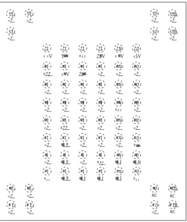
Figure 1.2 63-BGA Contact, x8 Device, Single CE (Top View) NC NC NC NC NC NC R/B# RE# CE# NC NC VCC VSS NC NC CLE ALE WE# WP# NC NC NC NC NC VSS NC NC NC I/O7 I/O6 I/O5 I/O4 NC VCC NC VCC VSS NC VCC NC I/O3 I/O2 I/O1 I/O0 NC NC NC VSS 12 13 37 36 25 48 1 24 NAND Flash TSOP1 (x8) (1) (1) (1) (1) F3 F4 F5 F6 F7 F8 E3 E4 E5 E6 E7 E8 D3 D4 D5 D6 D7 D8 C3 C4 C5 C6 C7 C8 RB# WE# CE# VSS ALE WP# NC NC NC CLE RE# VCC NC NC NC NC NC NC G3 G4 G5 G6 G7 G8 NC VSS NC NC NC NC H3 H4 H5 H6 H7 H8 Vcc NC NC NC I/O0 NC B9 A9 NC NC A2 NC NC NC NC NC VCC NC B10 A10 NC NC B1 A1 NC NC J3 J4 J5 J6 J7 J8 I/O7 I/O5 VCC NC I/O1 NC K3 K4 K5 K6 K7 K8 VSS I/O6 I/O4 I/O3 I/O2 VSS L9 NC L2 NC L10 NC L1 NC M9 NC M2 NC M10 NC M1 NC
2.
Pin Description
Notes:
1. A 0.1 µF capacitor should be connected between the VCC Supply Voltage pin and the VSS Ground pin to decouple the current surges from
the power supply. The PCB track widths must be sufficient to carry the currents required during program and erase operations. 2. An internal voltage detector disables all functions whenever VCC is below 1.8V to protect the device from any involuntary program/erase
during power transitions.
3.
Block Diagrams
Figure 3.1 Functional Block Diagram — 8 Gb
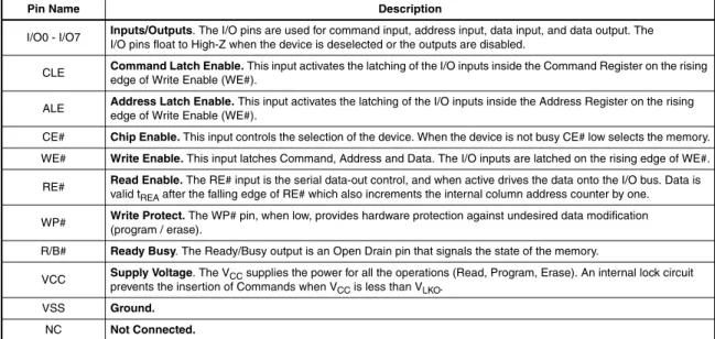
Table 2.1 Pin Description
Pin Name Description
I/O0 - I/O7 Inputs/Outputs. The I/O pins are used for command input, address input, data input, and data output. The I/O pins float to High-Z when the device is deselected or the outputs are disabled.
CLE Command Latch Enable. This input activates the latching of the I/O inputs inside the Command Register on the rising edge of Write Enable (WE#).
ALE Address Latch Enable. This input activates the latching of the I/O inputs inside the Address Register on the rising edge of Write Enable (WE#).
CE# Chip Enable. This input controls the selection of the device. When the device is not busy CE# low selects the memory. WE# Write Enable. This input latches Command, Address and Data. The I/O inputs are latched on the rising edge of WE#. RE# Read Enable. The RE# input is the serial data-out control, and when active drives the data onto the I/O bus. Data is
valid tREA after the falling edge of RE# which also increments the internal column address counter by one.
WP# Write Protect. The WP# pin, when low, provides hardware protection against undesired data modification (program / erase).
R/B# Ready Busy. The Ready/Busy output is an Open Drain pin that signals the state of the memory.
VCC Supply Voltage. The VCC supplies the power for all the operations (Read, Program, Erase). An internal lock circuit prevents the insertion of Commands when VCC is less than VLKO.
VSS Ground. NC Not Connected. Address Register/ Counter Controller Command Interface Logic Command Register Data Register RE# I/O Buffer Y Decoder Page Buffer X D E C O D E R NAND Flash Memory Array WP# CE# WE# CLE ALE I/O0~I/O7 Program Erase
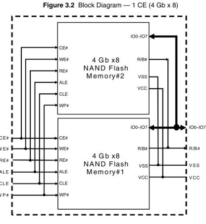
Figure 3.2 Block Diagram — 1 CE (4 Gb x 8)
4.
Addressing
Notes:
1. CAx = Column Address bit. 2. PAx = Page Address bit. 3. PLA0 = Plane Address bit zero. 4. BAx = Block Address bit.
5. Block address concatenated with page address and plane address = actual page address, also known as the row address. 6. A30 for 8 Gb (4 Gb x 2 – DDP) (1CE).
For the address bits, the following rules apply: A0 - A11: column address in the page A12 - A17: page address in the block
A18: plane address (for multiplane operations) / block address (for normal operations) A19 - A30: block address
IO0~IO7 CE# WE# R/B# RE# VSS ALE VCC CLE WP#
IO0~IO7 IO0~IO7
C E# CE# W E# WE# R/B# R /B # R E# RE# VSS VS S A L E ALE VCC V C C C L E CLE W P # WP# 4 Gb x8 N A N D F lash M em o ry#1 4 Gb x8 N A N D F lash M em o ry#2
Table 4.1 Address Cycle Map
Bus Cycle I/O0 I/O1 I/O2 I/O3 I/O4 I/O5 I/O6 I/O7
1st / Col. Add. 1 A0 (CA0) A1 (CA1) A2 (CA2) A3 (CA3) A4 (CA4) A5 (CA5) A6 (CA6) A7 (CA7) 2nd / Col. Add. 2 A8 (CA8) A9 (CA9) A10 (CA10) A11 (CA11) Low Low Low Low 3rd / Row Add. 1 A12 (PA0) A13 (PA1) A14 (PA2) A15 (PA3) A16 (PA4) A17 (PA5) A18 (PLA0) A19 (BA0) 4th / Row Add. 2 A20 (BA1) A21 (BA2) A22 (BA3) A23 (BA4) A24 (BA5) A25 (BA6) A26 (BA7) A27 (BA8) 5th / Row Add. 3
5.
Read Status Enhanced
Read Status Enhanced is used to retrieve the status value for a previous operation in the following cases: In the case of concurrent operations on a multi-die stack.
When two dies are stacked to form a dual-die package (DDP), it is possible to run one operation on the first die, then activate a different operation on the second die, for example: Erase while Read, Read while Program, etc.
In the case of multiplane operations in the same die.
6.
Read ID
The device contains a product identification mode, initiated by writing 90h to the command register, followed by an address input of 00h.
Note: If you want to execute Read Status command (0x70) after Read ID sequence, you should input dummy command (0x00) before Read Status command (0x70).
For the S34ML08G2 device, five read cycles sequentially output the manufacturer code (01h), and the device code and 3rd, 4th, and 5th cycle ID, respectively. The command register remains in Read ID mode until further commands are issued to it.
Figure 6.1 Read ID Operation Timing — 8 Gb
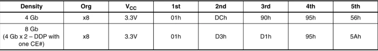
Table 6.1 Read ID for Supported Configurations
Density Org VCC 1st 2nd 3rd 4th 5th 4 Gb x8 3.3V 01h DCh 90h 95h 56h 8 Gb (4 Gb x 2 – DDP with one CE#) x8 3.3V 01h D3h D1h 95h 5Ah CE# WE# CLE RE# ALE tWHR tAR tREA Read ID Command Address 1 Cycle Maker Code Device Code
3rd Cycle 4th Cycle 5th Cycle
5th
ID Data
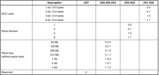
Table 6.2 Read ID Byte 5 Description
Description I/O7 I/O6 I/O5 I/O4 I/O3 I/O2 I/O1 I/O0
ECC Level 1 bit / 512 bytes 2 bit / 512 bytes 4 bit / 512 bytes 8 bit / 512 bytes 0 0 0 1 1 0 1 1 Plane Number 1 2 4 8 0 0 0 1 1 0 1 1 Plane Size (without spare area)
64 Mb 128 Mb 256 Mb 512 Mb 1 Gb 2 Gb 4 Gb 0 0 0 0 0 1 0 1 0 0 1 1 1 0 0 1 0 1 1 1 0 Reserved 0
6.1
Read Parameter Page
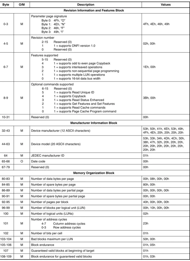
The device supports the ONFI Read Parameter Page operation, initiated by writing ECh to the command register, followed by an address input of 00h. The command register remains in Parameter Page mode until further commands are issued to it. Table 6.3 explains the parameter fields.
Table 6.3 Parameter Page Description (Sheet 1 of 2)
Byte O/M Description Values
Revision Information and Features Block
0-3 M
Parameter page signature Byte 0: 4Fh, “O” Byte 1: 4Eh, “N” Byte 2: 46h, “F” Byte 3: 49h, “I” 4Fh, 4Eh, 46h, 49h 4-5 M Revision number 2-15 Reserved (0)
1 1 = supports ONFI version 1.0 0 Reserved (0)
02h, 00h
6-7 M
Features supported
5-15 Reserved (0)
4 1 = supports odd to even page Copyback 3 1 = supports interleaved operations
2 1 = supports non-sequential page programming 1 1 = supports multiple LUN operations 0 1 = supports 16-bit data bus width
1Eh, 00h
8-9 M
Optional commands supported 6-15 Reserved (0)
5 1 = supports Read Unique ID 4 1 = supports Copyback
3 1 = supports Read Status Enhanced 2 1 = supports Get Features and Set Features 1 1 = supports Read Cache commands 0 1 = supports Page Cache Program command
3Bh, 00h
10-31 Reserved (0) 00h
Manufacturer Information Block
32-43 M Device manufacturer (12 ASCII characters) 53h, 50h, 41h, 4Eh, 53h, 49h, 4Fh, 4Eh, 20h, 20h, 20h, 20h
44-63 M Device model (20 ASCII characters)
53h, 33h, 34h, 4Dh, 4Ch, 30h, 38h, 47h, 32h, 20h, 20h, 20h, 20h, 20h, 20h, 20h, 20h, 20h, 20h, 20h 64 M JEDEC manufacturer ID 01h 65-66 O Date code 00h 67-79 Reserved (0) 00h
Memory Organization Block
80-83 M Number of data bytes per page 00h, 08h, 00h, 00h 84-85 M Number of spare bytes per page 80h, 00h 86-89 M Number of data bytes per partial page 00h, 00h, 00h, 00h 90-91 M Number of spare bytes per partial page 00h, 00h 92-95 M Number of pages per block 40h, 00h, 00h, 00h 96-99 M Number of blocks per logical unit (LUN) 00h, 10h, 00h, 00h
100 M Number of logical units (LUNs) 02h
101 M
Number of address cycles
4-7 Column address cycles 0-3 Row address cycles
23h
102 M Number of bits per cell 01h 103-104 M Bad blocks maximum per LUN 50h, 00h 105-106 M Block endurance 01h, 05h
Note:
1. “O” Stands for Optional, “M” for Mandatory.
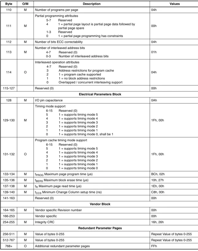
110 M Number of programs per page 04h
111 M
Partial programming attributes 5-7 Reserved
4 1 = partial page layout is partial page data followed by partial page spare
1-3 Reserved
0 1 = partial page programming has constraints
00h
112 M Number of bits ECC correctability 04h
113 M
Number of interleaved address bits 4-7 Reserved (0)
0-3 Number of interleaved address bits
01h
114 O
Interleaved operation attributes 4-7 Reserved (0)
3 Address restrictions for program cache 2 1 = program cache supported 1 1 = no block address restrictions
0 Overlapped / concurrent interleaving support
04h
115-127 Reserved (0) 00h
Electrical Parameters Block
128 M I/O pin capacitance 0Ah
129-130 M
Timing mode support
6-15 Reserved (0) 5 1 = supports timing mode 5 4 1 = supports timing mode 4 3 1 = supports timing mode 3 2 1 = supports timing mode 2 1 1 = supports timing mode 1
0 1 = supports timing mode 0, shall be 1
1Fh, 00h
131-132 O
Program cache timing mode support 6-15 Reserved (0) 5 1 = supports timing mode 5 4 1 = supports timing mode 4 3 1 = supports timing mode 3 2 1 = supports timing mode 2 1 1 = supports timing mode 1 0 1 = supports timing mode 0
1Fh, 00h
133-134 M tPROG Maximum page program time (µs) BCh, 02h 135-136 M tBERS Maximum block erase time (µs) 10h, 27h
137-138 M tR Maximum page read time (µs) 1Eh, 00h
139-140 M tCCS Minimum Change Column setup time (ns) C8h, 00h
141-163 Reserved (0) 00h
Vendor Block
164-165 M Vendor specific Revision number 00h
166-253 Vendor specific 00h
254-255 M Integrity CRC 16h, 26h
Redundant Parameter Pages
256-511 M Value of bytes 0-255 Repeat Value of bytes 0-255 512-767 M Value of bytes 0-255 Repeat Value of bytes 0-255
768+ O Additional redundant parameter pages FFh
Table 6.3 Parameter Page Description (Sheet 2 of 2)
7.
Electrical Characteristics
7.1
Valid Blocks
Note:
1. Each 4 Gb has maximum 80 bad blocks.
7.2
DC Characteristics
Notes:
1. All VCCQ and VCC pins, and VSS and VSSQ pins respectively are shorted together.
2. Values listed in this table refer to the complete voltage range for VCC and VCCQ and to a single device in case of device stacking.
3. All current measurements are performed with a 0.1 µF capacitor connected between the VCC Supply Voltage pin and the VSS Ground pin.
4. Standby current measurement can be performed after the device has completed the initialization process at power up.
7.3
Pin Capacitance
Note:
1. For the stacked devices version the Input is 10 pF x [number of stacked chips] and the Input/Output is 10 pF x [number of stacked chips].
Table 7.1 Valid Blocks
Device Symbol Min Typ Max Unit
S34ML04G2 NVB 4016 — 4096 Blocks
S34ML08G2 NVB 8032 (1) — 8192 Blocks
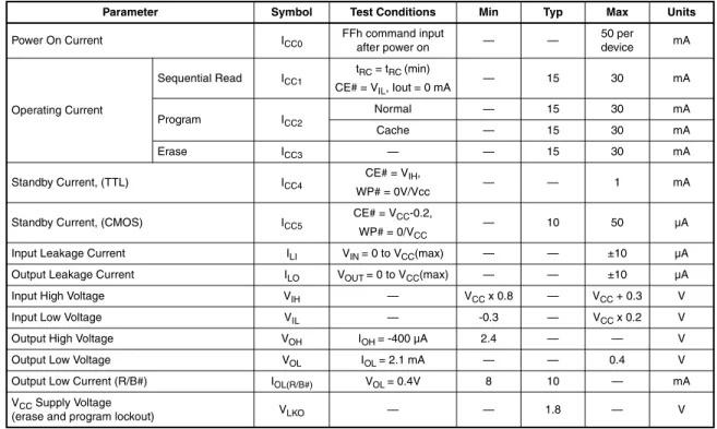
Table 7.2 DC Characteristics and Operating Conditions
Parameter Symbol Test Conditions Min Typ Max Units
Power On Current ICC0 FFh command input after power on — — 50 per device mA
Operating Current Sequential Read ICC1 tRC = tRC (min) CE# = VIL, Iout = 0 mA — 15 30 mA Program ICC2 Normal — 15 30 mA Cache — 15 30 mA Erase ICC3 — — 15 30 mA Standby Current, (TTL) ICC4 CE# = VIH, WP# = 0V/Vcc — — 1 mA
Standby Current, (CMOS) ICC5
CE# = VCC-0.2,
WP# = 0/VCC — 10 50 µA Input Leakage Current ILI VIN = 0 to VCC(max) — — ±10 µA
Output Leakage Current ILO VOUT = 0 to VCC(max) — — ±10 µA Input High Voltage VIH — VCC x 0.8 — VCC + 0.3 V
Input Low Voltage VIL — -0.3 — VCC x 0.2 V
Output High Voltage VOH IOH = -400 µA 2.4 — — V
Output Low Voltage VOL IOL = 2.1 mA — — 0.4 V Output Low Current (R/B#) IOL(R/B#) VOL = 0.4V 8 10 — mA
VCC Supply Voltage
(erase and program lockout) VLKO — — 1.8 — V
Table 7.3 Pin Capacitance (TA = 25°C, f=1.0 MHz)
Parameter Symbol Test Condition Min Max Unit
Input CIN VIN = 0V — 10 pF
7.4
Power Consumptions and Pin Capacitance for Allowed Stacking
Configurations
When multiple dies are stacked in the same package, the power consumption of the stack will increase according to the number of chips. As an example, the standby current is the sum of the standby currents of all the chips, while the active power consumption depends on the number of chips concurrently executing different operations.
When multiple dies are stacked in the same package the pin/ball capacitance for the single input and the single input/output of the combo package must be calculated based on the number of chips sharing that input or that pin/ball.
8.
Physical Interface
8.1
Physical Diagram
8.1.1
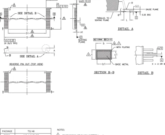
48-Pin Thin Small Outline Package (TSOP1)
Figure 8.1 TS2 48 — 48-lead Plastic Thin Small Outline, 12 x 20 mm, Package Outline
5007 \ f16-038 \ 6.5.13 PACKAGE TS2 48
JEDEC MO-142 (D) DD SYMBOL MIN NOM MAX
A --- --- 1.20 A1 0.05 --- 0.15 A2 0.95 1.00 1.05 b1 0.17 0.20 0.23 b 0.17 0.22 0.27 c1 0.10 --- 0.16 c 0.10 --- 0.21 D 19.80 20.00 20.20 D1 18.30 18.40 18.50 E 11.90 12.00 12.10 e 0.50 BASIC L 0.50 0.60 0.70 O 0˚ --- 8 R 0.08 --- 0.20 N 48 NOTES:
1. DIMENSIONS ARE IN MILLIMETERS (mm).
(DIMENSIONING AND TOLERANCING CONFORM TO ANSI Y14.5M-1994). 2. PIN 1 IDENTIFIER FOR STANDARD PIN OUT (DIE UP).
3. PIN 1 IDENTIFIER FOR REVERSE PIN OUT (DIE DOWN): INK OR LASER MARK. 4. TO BE DETERMINED AT THE SEATING PLANE -C- . THE SEATING PLANE IS
DEFINED AS THE PLANE OF CONTACT THAT IS MADE WHEN THE PACKAGE LEADS ARE ALLOWED TO REST FREELY ON A FLAT HORIZONTAL SURFACE.
5. DIMENSIONS D1 AND E DO NOT INCLUDE MOLD PROTRUSION. ALLOWABLE MOLD PROTRUSION ON E IS 0.15mm PER SIDE AND ON D1 IS 0.25mm PER SIDE. 6. DIMENSION b DOES NOT INCLUDE DAMBAR PROTRUSION. ALLOWABLE DAMBAR
PROTRUSION SHALL BE 0.08mm TOTAL IN EXCESS OF b DIMENSION AT MAX. MATERIAL CONDITION. DAMBAR CANNOT BE LOCATED ON LOWER RADIUS OR THE FOOT. MINIMUM SPACE BETWEEN PROTRUSION AND AN ADJACENT LEAD TO BE 0.07mm. 7. THESE DIMENSIONS APPLY TO THE FLAT SECTION OF THE LEAD BETWEEN
0.10mm AND 0.25mm FROM THE LEAD TIP.
8. LEAD COPLANARITY SHALL BE WITHIN 0.10mm AS MEASURED FROM THE SEATING PLANE.
8.1.2
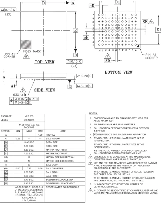
63-Pin Ball Grid Array (BGA)
Figure 8.2 VLD063 — 63-Pin BGA, 11 mm x 9 mm Package
g5013 \ 16-038.28 \ 6.5.13 NOTES:
1. DIMENSIONING AND TOLERANCING METHODS PER ASME Y14.5M-1994.
2. ALL DIMENSIONS ARE IN MILLIMETERS. 3. BALL POSITION DESIGNATION PER JEP95, SECTION 3, SPP-020.
4. e REPRESENTS THE SOLDER BALL GRID PITCH. 5. SYMBOL "MD" IS THE BALL MATRIX SIZE IN THE "D" DIRECTION.
SYMBOL "ME" IS THE BALL MATRIX SIZE IN THE "E" DIRECTION.
n IS THE TOTAL NUMBER OF POPULATED SOLDER BALL POSITIONS FOR MATRIX SIZE MD X ME. 6 DIMENSION "b" IS MEASURED AT THE MAXIMUM BALL
DIAMETER IN A PLANE PARALLEL TO DATUM C. 7 “SD” AND “SE” ARE MEASURED WITH RESPECT TO DATUMS
A AND B AND DEFINE THE POSITION OF THE CENTER SOLDER BALL IN THE OUTER ROW.
WHEN THERE IS AN ODD NUMBER OF SOLDER BALLS IN THE OUTER ROW “SD” OR “SE” = 0.
WHEN THERE IS AN EVEN NUMBER OF SOLDER BALLS IN THE OUTER ROW, “SD” = eD/2 AND “SE” = eE/2. 8. "+" INDICATES THE THEORETICAL CENTER OF DEPOPULATED BALLS.
9 A1 CORNER TO BE IDENTIFIED BY CHAMFER, LASER OR INK MARK, METALLIZED MARK INDENTATION OR OTHER MEANS.
PACKAGE VLD 063
JEDEC M0-207(M)
11.00 mm x 9.00 mm
PACKAGE
SYMBOL MIN NOM MAX NOTE
A --- --- 1.00 PROFILE A1 0.25 --- --- BALL HEIGHT D 11.00 BSC. BODY SIZE E 9.00 BSC. BODY SIZE D1 8.80 BSC. MATRIX FOOTPRINT E1 7.20 BSC. MATRIX FOOTPRINT
MD 12 MATRIX SIZE D DIRECTION
ME 10 MATRIX SIZE E DIRECTION
n 63 BALL COUNT
b 0.40 0.45 0.50 BALL DIAMETER eE 0.80 BSC. BALL PITCH eD 0.80 BSC. BALL PITCH
SD 0.40 BSC. SOLDER BALL PLACEMENT SE 0.40 BSC. SOLDER BALL PLACEMENT
A3-A8,B2-B8,C1,C2,C9,C10 DEPOPULATED SOLDER BALLS D1,D2,D9,D10,E1,E2,E9,E10
F1,F2,F9,F10,G1,G2,G9,G10 H1,H2,H9,H10,J1,J2,J9,J10 K1,K2,K9,K10 L3-L8,M3-M8
9.
Ordering Information
The ordering part number is formed by a valid combination of the following:
Valid Combinations
Valid Combinations list configurations planned to be supported in volume for this device. Consult your local sales office to confirm availability of specific valid combinations and to check on newly released
combinations.
S34ML 08G 2 01 T F I 00 0
Packing Type
0 = Tray 3 = 13” Tape and Reel
Model Number
00 = Standard Interface / ONFI (x8)
Temperature Range
I = Industrial (–40°C to + 85°C)
Materials Set
F = Lead (Pb)-free
H = Lead (Pb)-free and Low Halogen
Package
B = BGA T = TSOP
Bus Width
00 = x8 NAND, single die 04 = x16 NAND, single die 01 = x8 NAND, dual die
05 = x16 NAND, dual die
Technology
2 = Spansion NAND Revision 2 (32 nm)
Density 01G = 1 Gb 02G = 2 Gb 04G = 4 Gb 08G = 8 Gb Device Family S34ML
Spansion SLC NAND Flash Memory for Embedded
Valid Combinations Device
Family Density Technology Bus Width Package Type Temperature Range Additional Ordering Options Packing Type Package Description S34ML 08G 2 01 BH, TF I 00 0, 3 BGA, TSOP
10. Revision History
Section Description
Revision 01 (April 11, 2013)
Initial release
Revision 02 (May 17, 2013)
Performance Reliability: updated
Addressing Address Cycle Map table: updated Bus Cycle data
Read ID Read ID for Supported Configurations table: updated 8 Gb Density for 2nd, 3rd, 4th, and 5th Read Parameter Page Parameter Page Description table: corrected values for Bytes 8-9 and 254-255
Revision 03 (August 9, 2013)
Read ID Read ID Operation Timing — 8 Gb figure: added values to I/Ox
Physical Interface Updated TS2 48 — 48-lead Plastic Thin Small Outline, 12 x 20 mm, Package Outline figure
Revision 04 (January 8, 2015)
Performance Package Options: added 63-Ball BGA 11 x 9 x 1 mm Connection Diagram Added figure: 63-BGA Contact, x8 Device, Single CE Physical Interface Added 63-Pin Ball Grid Array (BGA)
Colophon
The products described in this document are designed, developed and manufactured as contemplated for general use, including without limitation, ordinary industrial use, general office use, personal use, and household use, but are not designed, developed and manufactured as contemplated (1) for any use that includes fatal risks or dangers that, unless extremely high safety is secured, could have a serious effect to the public, and could lead directly to death, personal injury, severe physical damage or other loss (i.e., nuclear reaction control in nuclear facility, aircraft flight control, air traffic control, mass transport control, medical life support system, missile launch control in weapon system), or (2) for any use where chance of failure is intolerable (i.e., submersible repeater and artificial satellite). Please note that Spansion will not be liable to you and/or any third party for any claims or damages arising in connection with above-mentioned uses of the products. Any semiconductor devices have an inherent chance of failure. You must protect against injury, damage or loss from such failures by incorporating safety design measures into your facility and equipment such as redundancy, fire protection, and prevention of over-current levels and other abnormal operating conditions. If any products described in this document represent goods or technologies subject to certain restrictions on export under the Foreign Exchange and Foreign Trade Law of Japan, the US Export Administration Regulations or the applicable laws of any other country, the prior authorization by the respective government entity will be required for export of those products.
Trademarks and Notice
The contents of this document are subject to change without notice. This document may contain information on a Spansion product under development by Spansion. Spansion reserves the right to change or discontinue work on any product without notice. The information in this document is provided as is without warranty or guarantee of any kind as to its accuracy, completeness, operability, fitness for particular purpose, merchantability, non-infringement of third-party rights, or any other warranty, express, implied, or statutory. Spansion assumes no liability for any damages of any kind arising out of the use of the information in this document.