AbstractDynamic Voltage Restorer (DVR) is a power electronics device to protect sensitive load when voltage sag occurs. Commonly, sensitive loads are electronic-based devices which generate harmonics. The magnitude and phase of compensated voltage in DVR depend on grounding system and type of fault. If the system is floating, the zero sequence components do not appear on the load side. Meanwhile, in a neutral grounded system, voltage sag is extremely affected by zero sequence components. A blocking transformer is commonly installed in series with DVR to reduce the effect of zero sequence components. This paper proposes a new DVR control scheme that is capable of eliminating the blocking transformer and reducing harmonic distortion. The system uses fuzzy polar controller to replace the conventional PI or FL controller that is commonly used. By taking into account the zero sequence components in the controller design, the effects of zero sequence components can be compensated. Simulated results show the effectiveness of the proposed DVR controller
KeywordsVoltage sag, DVR, zero sequence compo-nents, harmonic, fuzzy polar.
I.INTRODUCTION
ccording to EPRI report, the revenue losses due to poor power quality in U.S. business were $400 billion per year (John 1998). Power quality problems occur due to dynamic or non-linear loads and interaction between the load and network. Two main problems in the field of power quality can be categorized as voltage sag and instantaneous power loss. In addition, voltage sag has two main parameters including magnitude and time duration (Zang 2004). DVR (Dynamic Voltage Restorer) is a device that can be used to mitigate instantaneous voltage sag. Most of the works in DVR designs are neglecting the effects of zero sequence components (Haddad 1997, Campos 1994). Under the foregoing assumption, only the restoration of positive-sequence and the compensation of negative positive-sequence are taken into consideration, while zero-sequence compo-nents are ignored. In some cases, however, the effects of zero sequence components cannot be neglected. Thus the influence of the zero-sequence components must be considered in a DVR design (Bollen 1999).
1Margo P, M Heri P, M Ashari, and Zaenal P are with Department of
Electrical Engineering, Faculty of Industrial Technology, Institut Teknologi Sepuluh Nopember, Surabaya, 60111, Indonesia. E-mail: [email protected].
2
Takashi Hiyama is with the Department of Electrical Engineering and Computer Science, Kumamoto University, Japan. E-mail: [email protected].
In a high power source of 3 phase – 3 wire grounded system, the zero sequence component may not affect the line to line voltages. However, in a limited power source, the zero sequence components will affect the line voltage. To minimize the effects of zero sequence components, a delta-wye transformer (blocking trans-former) is generally used in DVR installation, as shown in Fig. 1.
This paper proposes a DVR controller based on Fuzzy Polar Control Scheme that having capabilities to minimize effects of zero sequence voltage component and voltage harmonics. The method eliminates the need of using a delta-wye blocking transformer, resulting in more economical system. In order to take into account the effects of zero sequence components, the proposed
DVR controller is using d-q-0 transformation in the
design. The proposed DVR is also designed as a harmonic isolator to block the harmonic currents from nonlinear load to mains. Simulated results show the effectiveness of the proposed DVR controller.
II.VOLTAGE SAG IN DISTRIBUTION SYSTEM
According to IEEE Standard, the voltage sags is defined as RMS variation with the magnitude between 10% and 90% of nominal voltage and the duration is between 0.5 cycles to one minute. Voltage sags are affected by fault such as short circuits, overloads and starting of large motor. The phenomenon of voltage sags are the most common disturbance in the power system which certainly gives the effects especially to the several type of equipments such as adjustable speed drives, control equipment, and computers are notorious for their sensitivity (Pujiantara 2007). The model of distribution system used in this study can be depicted in Fig. 2. This is a model of grounded radial distribution networks.
Rating of the power plant is 10 MW (100 MVASC), 6.6 kV, while both feeder impedances consist of
resistance R = 0.2024 Ohm and inductance L = 2.84 mH.
The normal load power is 4 MW, Q = 1 MVAR.
Sensitive loads are 5 MW with the value of Q is 1
MVAR. Rectifier load is included at the sensitive loads. As we know that the most faults occurred in the power systems are single phase to ground. Whenever a single fault occurs in the normal load bus feeder, the sensitive load feeder will suffer from voltage sag. The voltage phasor diagram under single phase faults is depicted in Fig. 3. The voltages in the sensitive load bus before a fault occurs can be explained by the following equations (in pu):
Advanced DVR with Zero-Sequence Voltage
Component and Voltage Harmonic Elimination
for Three-Phase Three-Wire Distribution
Systems
Margo P.
1, M. Heri P.
1, M. Ashari
1, Zaenal P.
1, and Takashi Hiyama
23 3 2 1 2 1 3 2 1 2 1 1 j V j V V c b a (1)
Under single phase fault, the voltage equations became as follows: 3 2 1 2 1 3 2 1 2 1 j V j V sin jV cos V V c b
a (2)
where V is the magnitude of voltage sag and is phase
angle jump. Then, the zero sequence components during fault can be obtained by the following equation:
) (
3
1
Va Vb Vc
o V ) 1 sin cos ( 3 1 jV V Vo (3)
In (3), the resultant of three vectors are not zero, it means that zero sequence voltage is generated during ground fault. Therefore the process of eliminating the zero sequence components is required.
III.DYNAMIC VOLTAGE RESTORER
Fig. 4 shows the scheme of proposed DVR. The DVR has two controllers, sag control unit and harmonic control unit. The DVR dynamically injects a controlled voltage in series to the bus voltage by means of a booster transformer. There are three single phase booster transformers connected to a three phase converter with energy storage system and control circuit. The amplitudes of the three injected phase voltages are controlled such as to eliminate any detrimental effects of a bus fault to the load voltage. This means that any differential voltage caused by transient disturbances in the ac feeder will be compensated by an equivalent voltage generated by the converter and injected on the medium voltage level through the booster transformer.
The basic mathematical expression of the injection voltage from the ideal DVR can expressed using the following equation.
sag ref
inj V V
V
(4)
where Vinj is DVR injection voltage, Vrefis reference
pre-fault voltage and Vsag is the voltage sags. The
mathematical expression of the ideal DVR can be illustrated in a phasor diagram as depicted in Fig. 5.
A. Conventional Control Scheme
The simple conventional control scheme of DVR can
be seen in Fig. 6. In this scheme the d-q model is
utilized. The three phases voltage from the power
sources is converted to d-q model. Transformation from
a-b-c to d-q axis is a easy way to control the system.
Controlling the system using the d-q model also avoids
the time delay inherent in working with root mean square
phasor values. Thevalue of parameters Vd ref and Vq ref
are 1 and 0 respectively. Conventional DVRs mostly use Δ-Y transformer (blocking transformer) to reduce the zero sequence impedance and therefore, the zero sequence voltage during ground fault is almost zero. The
conversion of a-b-c to d-q-0 axis is shown in Eqs. (5). In
conventional DVR controllers, the existence of zero sequence components is not taken into account.
c v b v a v . q v d v v t cos t cos t cos t sin t sin t sin 3 2 3 2 3 2 3 2 2 1 2 1 2 1 3 2 0 (5)
As the effects of zero sequence components are neglected in conventional DVR controllers, the voltages of sensitive loads cannot be restored completely during single-phase faults. A blocking transformer must be used if a complete restoration is desirable.
B. Proposed Control Scheme
The proposed control scheme of DVR in simplified block diagram can be seen in Fig. 7. There are two differences with conventional scheme. First, the
proposed method compensates d, q and 0 axis, while
conventional scheme only compensate d and q axis.
Second, this paper utilizes a fuzzy polar method to improve the performance of conventional PI controller (Pujiantara 2008, Jurando 2003, Ortmeyer 1995). Fuzzy polar method have been developed for the application of control on electric power systems (Ortmeyer 1995, Hiyama 1994, Hiyama 1991). However, fuzzy polar has never been use in DVR control scheme. This controller is suitable for DVR control because it has two membership functions only. It is provide a simple design approach.
The method to restore the voltage sag is determined from the comparison between the real time voltage from
the line in a-b-c form which is converted to d-q-0 axis
and the values of d-q-0 references. The value of
reference voltages are defined as Vdref, Vqref and V0ref are
1, 0 and 0 respectively.
The voltage difference measured in the system is defined as the error signal which shows the value of
voltage drop V. Here, it is clearly explained that not
only d-q voltage is being compensated that many
researches did, but also the components of d, q, and 0.
Here, the fuzzy polar consists of 3 basic parameters:
derivative multiplier (As), the angle membership
function (, and radius membership function (Dr). The
mechanisms of operation of polar coordinates are shown in Eqs. 7 to 9.
p(k) = [Zs(k) AsZa(k)] (7)
2 2 )) ( . ( ) ( )
(k Zsk AsZak
D (8)
(k) = tan-1(As.Za(k)/Zs(k)) (9)
Given the input signal Zs, the controller need the
signal derivative to get Za. Point p(k) is represented by
input Zs as x axis and As.Za as y axis. To be used for
fuzzy polar controller, input form p(k) in rectangular
form should be transformed to polar form, D(k) as
magnitude and (k) is the angle. The polar form of fuzzy
polar is shown in Fig. 8.
The other factors which is also needed in this control
system is maximum control signal Umax.
Defuzzification rule as fuzzy polar output (U) for the
control system is shown in equation 10.
U(k) = G(D(k)) [N((k)) – P((k))]Umax (10)
Where Umax is the maximum allowable control signal.
G(D(k)) is the membership value of magnitude D(k),
while N((k)) and P((k)) are membership value of the
Membership function of fuzzy polar is shown in Fig. 9. Error signal ∆Vd, ∆Vd’, ∆Vq, ∆Vq’, ∆V0, and ∆V0’ are
then transformed to polar d-q-0 form using Eqs. 7, 8, and
9 respectively. The result becomes the input of fuzzy polar control. Fig. 10 is the simple model of fuzzy polar with 1 input and 1 output. In reality, there is only one
input, Zs. But it needs derivative signal Za so that it can
be converted to polar coordinate by Eqs 7, 8, 9 respectively.
Dr obtained from maximum deviation direct input
∆Vd, quadrature input ∆Vq and zero input ∆V0. Maximum
parameters deviation is 1, α = 90º. As obtained from trial
and error. Umax is very important parameter. From Eqs.
(10), U(k)max = 1. Then Umax is shown in Eqs. 11.
Result of these parameters summarized at table 1.
min ))] ( ( )) ( ( ))[ ( (
1 k P k N k D G max U
Result of error compensation from fuzzy polar control is control signal which shows the value of the voltage will be injected to the system by the inverter.
C. DVR as Voltage Harmonics Compensator
Refer to Fig. 4, DVR control as voltage harmonics compensator is similar to that of as sag compensator. Its difference is voltage feedback side. In sag compensator the feedback voltage is the measured voltage before the booster (source side), while in harmonics compensator the feedback voltage is the load side harmonics voltage. The proposed control scheme of harmonics eliminator simplified block diagram can be seen in Fig. 11. So, by using this method, all distortion signal caused by harmonics will be compensated. Using this method, voltage harmonics generated by sensitive load will not propagate to the source.
Compensation of harmonics voltage injected by DVR to the system is shown in equations 12, 13, 14.
Vdh= Vdact - Vdf (12)
Vqh = Vqact - Vqf (13)
V0h = V0act – V0f (14)
The values of harmonics voltages Vdh, Vqh, V0h are
obtained by comparing measured voltages Vdact, Vqact,
V0act with fundamental voltages (50 hz) Vdf, Vqf, V0f. The
value of fundamental voltage Vdf = 1, Vqf = 0, and V0f= 0.
Fig. 11 shows that harmonics voltages Vdh, Vqh, V0h
need the signal derivative to get Vdh’, Vqh’ and V0h’. Point p(k) is represented by input Vdh, Vqh, V0h as x axis and As.Vdh’, As.Vqh’ and As.V0h’ as y axis. To be used for
fuzzy polar controller, input form p(k) in rectangular
form should be transformed to polar form, D(k) as
magnitude and (k) is the angle. Equations 15, 16 and 17
show polar magnitude for harmonics input controller. 2
2
)) ( ' . ( ) ( )
(k V k A V k
Ddh dh s dh
(15) 2
2
)) ( ' . ( ) ( )
(k V k A V k
Dqh qh s qh
(16) 2
0 2
0
0 (k) V (k) (A.V '(k))
Dh h s h
(17) Equations 18, 19 and 20 show polar angle for harmonics input controller.
) (
) ( ' . ) (
k V
k V A k
dh dh s
dh
(18)
) (
) ( ' . ) (
k V
k V A k
qh qh s
qh
(19)
) (
) ( ' . ) (
k V
k V A k
dh dh s
dh
Then process to determination other parameters are equal to process sagging restorer.
IV.SIMULATED RESULTS
Simulation is done by using Matlab SimPower System. Parameters of fuzzy polar are shown in Table 1 and Table 2. It is simulated that a short circuit fault occurs in normal load bus (Fig. 2) for 2 cycles, which causes voltage sag in sensitive load bus. Sensitive load is usually nonlinear loads that generate harmonics. DVR installation in sensitive load feeder is intended to restore the voltage which is distorted by sag and harmonics.
A. Under Sag Condition
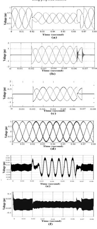
To see the proposed control scheme performance, sags of 30%, 50%, and 70% in sensitive load bus will be simulated. Voltage sag caused by two phase to ground fault, conventional DVR compensation waveform and proposed DVR compensation waveform are shows in Fig. 12 (a), Fig. 12 (b) and Fig. 12 (c). The fault use in this figure is two phase to ground because it represents the highest unbalance sag. Fig. 12 (b) shows that DVR compensation waveform using conventional control scheme is not perfect. The DVR compensation is 3 phase. There is should be only 2 phase because sagging fault is 2 phase to ground fault. This compensation cause unbalanced voltage at sensitive load. From Fig. 12 (c) can be seen that DVR compensation waveform using proposed control scheme is perfect. There are only 2 phase compensations. Proposed DVR control scheme is able to restore the voltage up to 99.08 % as seen in Fig. 12 (d). Fig. 12 (e) shows the value of zero sequence voltage in sensitive load bus using conventional DVR control scheme. It means that the conventional DVR control is unable to reduce zero the sequence voltage while sag voltage caused by ground fault occurs. Fig. 12 (f) shows the value of zero sequence voltage at sensitive load bus using proposed control scheme. It means that the proposed DVR control able to compensate the voltage sag including zero sequence components. From Fig. 12 (e) and Fig. 12 (f) can be seen that the value of zero sequence voltage decreases from 0.3 pu to 0.04 pu. DVR proposed method is able to reduce the zero sequence components.
Symmetrical voltage sag caused by three phase fault,
conventional DVR compensation waveform and
proposed DVR compensation waveform are shows in Fig. 13 (a), Fig. 13 (b) and Fig. 13 (c). From Fig. 13 (b) and Fig. 13 (c) show that DVR compensation waveform using both conventional and proposed control scheme are able to compensate symmetrical voltage sag.
Proposed DVR control scheme can restore the voltage up to 99.02 % as seen in Fig. 13 (d). Fig. 13 (e) shows the value of zero sequence voltage in sensitive load bus using conventional DVR control scheme. During fault conventional DVR control gives small injection of zero components about 0.1 pu. Fig.13 (f) shows the value of zero sequence voltage at sensitive load bus using proposed control scheme. During fault, proposed DVR control scheme gives very small injection of zero components about 0.03 pu. That means proposed DVR control scheme not injects the zero sequence components (11)
while symmetrical voltage sag caused by three phase fault occurs.
VLL of sag voltage caused by single phase to ground
fault, VLL sensitive load restored by conventional control
scheme and VLL sensitive load restored by proposed
control scheme shown at Fig. 14. Fig. 14 (b) and Fig. 14 (c) show that DVR waveform using both conventional and proposed control scheme are able to compensate single phase to ground fault voltage sag. But, Table 3 shows that restore by conventional method in case of 30% sag due to single phase to ground fault causes voltage line to ground rise up to 123.65 %. In same case shows that restore by proposed method voltage line to ground becoming 99.3 %. Compare to the conventional scheme, proposed scheme gave lower voltage stress phase-to-ground.
Several types of fault have been simulated and the
result can be seen in Table 3. Vrestoration is defined as the
voltage at sensitive bus after DVR during fault happened. Table 3 shows that at line to ground voltage, the conventional DVR control scheme can restore only on symmetrical and asymmetrical without zero sequence voltage sag. While asymmetrical voltage sags caused by zero sequence components, conventional DVR control scheme can’t restore well. Table 3 also shows that at line to line voltage, both the conventional DVR control and proposed control scheme can restore on symmetrical and asymmetrical voltage sag.
Where the error is defined by
% 100
Vrestoration
Error
(21) Simulation results show that at line to ground and line to line voltage, DVR using proposed method can restore both symmetrical and asymmetrical voltage sags very well. Proposed method able to replaces the function of blocking transformer. Therefore the blocking transformer can be removed, resulting in more economical system.
B. Operation as Harmonic Isolator
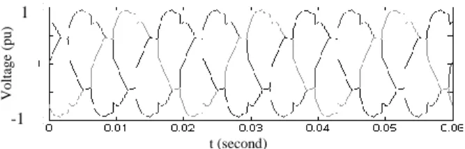
Fig. 15 shows voltage profile at sensitive load bus which is distorted by harmonics. Fig. 16 shows voltage profile at sensitive load bus after fuzzy polar DVR installation. Voltage profile in Fig. 17, has THD of 12.16%. After voltage restoration using fuzzy polar DVR, THD decreases to 1.95%.
IV.CONCLUSION
DVR with the technique of zero sequence elimination at distribution system 3 phase 3 wire using neutral grounding was modeled by Matlab SimPower System and fault caused by zero sequence in distribution system was simulated and analyzed. Also, the effects of zero-sequence components were simulated and discussed. Therefore the proposed system can be an alternative for system previously using blocking transformer. Proposed method able to replaces the function of blocking
transformer, resulting in more economical system. Moreover, compare to the conventional scheme, proposed scheme gave lower voltage stress phase-to-ground. And DVR can compensate the voltage harmonics as well.
Simulation results show that DVR using this method can restore both symmetrical and asymmetrical voltage sags very well. The average error of DVR voltage sag compensation is 0.99% at line to ground voltage and 0.84 at line to line voltage. Under normal condition, DVR is able to decrease voltage THD from 12.16% to 1.95%. This method can be adapted to the conventional DVR model.
REFERENCES
[1] M. H. J. Bollen, 1999, Understanding Power Quality Problems:
Voltage Sags and Interruptions, New York, IEEE Press.
[2] A. Campos et al., 1994, ”Analysis and design of a series voltage
unbalance compensator based on three-phase VSI operating with
unbalanced switching function”, IEEE Trans. On Power
Electronics, vol. 9 no. 3, pp.269-274, May.
[3] John, S. Hsu, 1998, "Instantaneous Phasor method for obtaining
instantaneous balanced fundamental components for power
quality control and continuous diagnostics‖, IEEE Transactions
on Power Delivery, Vol.13, No.4, pp.1494-1500.
[4] F. Jurado and M. Valverde, 2003, ‖Voltage correction by
dynamic voltage restorer based on fuzzy logic controller‖, IEEE
Transaction on Industrial Electronics.
[5] K. Haddad and G. Joos, 1997, ‖Distribution system voltage
regulation under fault conditions using static series regulators‖, Proc. Conf. Annual Meeting, IEEE Ind. Appl. Soc.m pp. 1383-1389.
[6] T. Hiyama and T. Sameshima, 1991, ―Fuzzy logic control
scheme for on-line stabilization of multimachine power system‖, Fuzzy Sets and System, Vol. 39, No. 2 pp. 181-194.
[7] T. Hiyama, 1994, ―Real time control of micro-machine system
using microcomputer based fuzzy logic power system stabilizer‖, IEEE Trans. On Energy Conversion, Vol. 9, No.4, pp.724-731.
[8] T. Hiyama, 1994, ―Robustness of fuzzy logic power system
stabilizers applied to multimachine power systems‖, IEEE Trans.
on Energy Conversion, Vol. 9, No.3, pp.451-459.
[9] T. H. Ortmeyer and T. Hiyama, 1995, ―Frequency response
characteristics of the fuzzy polar power system stabilizer‖, IEEE
Transactions on Energy Conversion, Vol. 10, No.2.
[10] M. Pujiantara, M. H. Purnomo, M Ashari, and T. Hiyama, 2007,
―Balanced voltage sag correction using dynamic voltage restorer
based on fuzzy polar controller‖, ICICIC 2007 Conference
Proceedings, Kumamoto Japan.
[11] M. Pujiantara, M. H. Purnomo, M. Ashari, Zaenal P.A., and T.
Hiyama, 2008, ―Compensation of balanced and unbalanced voltage sags using dynamic voltage restorer based on fuzzy polar
controller‖, International Journal of Applied Engineering
Research (IJAER) – Research India Publications IJAER 455 Vol.3 No.7, Delhi India.
[12] Zhang, Lidong, and Math H.J.Bollen, 2004, ―Characteristic of
voltage dips (sags) in power system‖, IEEE Transaction on
Industrial Electronic. Appendix
Energy Storage Control
Sensitive Load
Booster Transformer
DVR Normal Load
Blocking Transformer
Fig. 1. A DVR installation using blocking transformer to minimize the effects of zero sequence components
DVR
Main Bus
Sensitive load Bus Normal load Bus
Grounding
Ground fault
Fig. 2. Model of distribution system
Va
Vb
Vc
V
Fig. 3. Voltage phasor diagram during single phase fault
VSI
Energy Storage Sag Control
Unit
Booster transformer
Source Load
Harmonic Control
Unit
Fig. 4. Block diagram of DVR System
Vref
Vsag Vinj
Fig. 5. Basic DVR phasor diagram
Vabc Vabc to dq Vd ref
PI controller
dq to abc
Vq ref V0=0
Vd
Vq
PWM +
+
-Fig. 6. Conventional DVR control scheme
Vabc
Vabc
to dq0
V0 ref
+
-Vd ref
+
Vq ref d dt
d dt
d dt
Fuzzy polar rules
V0 Vd
Vq
Vd‘
Vq‘
V0‘
dq0 to abc Vd
Vq
V0
PWM
-Fig. 7. Proposed DVR control scheme
Switching Line
Sector A
Sector B
D(k) p(k)
/2
(k) As.
45
/2
Za(k)
Zs(k)
O
Fig. 8. Phase plane of fuzzy logic controller with polar information
180 135 45
- 45 0 - 180 - 135
1
grade
) ( d
N P(d)
Degree
d
0.01 1
1
)) ( (D k
G d
grade
Magnitude )
(k Dd
90
Fig. 9. Fuzzy 1polar membership function
Rule
Fuzzy Polar
dt
d
U
Zs
Za
Input
Signal
146
IPTEK,
The Journal for Technology and Science, Vol. 20, No. 4, November 2009
Vabc Vabc to dq0 Vof + -Vdf + Vqf d dt d dt d dt Fuzzy polar rules Voh Vdh Vqh Vdh’ Vqh’ Voh’ dq0 to abc Vd Vq V0 PWM -Vqact Vdact VoactFig. 11. Harmonics eliminator simplified block diagram
TABLE 1
FUZZY POLAR PARAMETERS FOR SAG COMPENSATOR
No
Fuzzy Polar Parameter Direct
input d
Quadrature
input q
Zero
input 0
1. As 0.19 0.19 0.19
2. Dr 1 1 1
3. α 90º 90º 90º
4. Umax 4.7 4.5 4.3
TABLE 2
FUZZY POLAR PARAMETERS FOR HARMONICS COMPENSATOR
No
Fuzzy Polar Parameter Direct input
d
Quadrature
input q
Zero input 0
1. As 0.19 0.19 0.19
2. Dr 0.8 0.8 1
3. α 90º 90º 90º
4. Umax 65 73 27
V ol ta ge (p u) Time (second) Time (second) V ol ta ge (p u) -2 2 -1 1
0 0.01 0.02 0.03 0.04 0.05 0.06 0.07 0.08
V ol ta ge (p u) Time (second) Time (second) V ol ta ge (p u) 0.1 -0.3 -0.2 -0.1 0.3 0.2
0 0.01 0.02 0.03 0.04 0.05 0.06 0.07 0.08
V ol ta ge (p u) Time (second) 1 2 -1 -2 V ol ta ge (p u) Time (second)
0 0.01 0.02 0.03 0.04 0.05 0.06 0.07 0.08
(c) (d) (a) (b) (f) (e) 0 Vo lta ge (p u) Time (second) Time (second) Vo lta ge (p u) -2 2 -1 1
0 0.01 0.02 0.03 0.04 0.05 0.06 0.07 0.08
Vo lta ge (p u) Time (second) Time (second) Vo lta ge (p u)0.1 -0.3 -0.2 -0.1 0.3 0.2
0 0.01 0.02 0.03 0.04 0.05 0.06 0.07 0.08
Vo lta ge (p u) Time (second) 1 2 -1 -2 Vo lta ge (p u) Time (second)
0 0.01 0.02 0.03 0.04 0.05 0.06 0.07 0.08
(c) (d) (a) (b) (f) (e) 0
Fig. 12. Case of 50% sag due to two phase to ground fault, (a) Line voltage, (b) Compensation voltage using conventional method. (c) Compensation voltage using proposed method, (d) Sensitive load bus
voltage Vo Time (second) Time (second) Vo lta ge (p u) -2 2 -1 1
0 0.01 0.02 0.03 0.04 0.05 0.06 0.07 0.08
Vo Time (second) Time (second) Vo lta ge (p u)0.1 -0.3 -0.2 -0.1 0.3 0.2
0 0.01 0.02 0.03 0.04 0.05 0.06 0.07 0.08
Vo lta ge (p u) Time (second) 1 2 -1 -2 Vo lta ge (p u) Time (second)
0 0.01 0.02 0.03 0.04 0.05 0.06 0.07 0.08
(c) (d) (a) (b) (f) (e) 0
Fig. 13. Case of 50% sag due to two phase to ground fault, (e) Zero sequence voltage using conventional method, (f) Zero sequence voltage
using proposed method
Vo lta ge (p u) Time (second) Time (second) Vo lta ge (p u) -2 2 -1 1 Time (second) Time (second) 0.08 (c) (d) (a) (b) (f) (e) 1 2 -1 -2 Vo lta ge (p u) Time (second)
0 0.01 0.02 0.03 0.04 0.05 0.06 0.07
0.5 -0.5 Vo lta ge (p u) Time (second) Vo lta ge (p u)0.04 -0.02 0.1 0.08
0 0.01 0.02 0.03 0.04 0.05 0.06 0.07 0.08
0.06 0.02 -0.04 -0.06 -0.08 -0.1 Vo lta ge (p u)0.05 -0.05 0.1 -0.1
0 0.01 0.02 0.03 0.04 0.05 0.06 0.07 0.08
0 0.01 0.02 0.03 0.04 0.05 0.06 0.07 0.08
V ol ta ge (p u) Time (second) Time (second) V ol ta ge (p u) -2 2 -1 1 Time (second) Time (second) 0.08 (c) (d) (a) (b) (f) (e) 1 2 -1 -2 V ol ta ge (p u) Time (second)
0 0.01 0.02 0.03 0.04 0.05 0.06 0.07
0.5 -0.5 V ol ta ge (p u) Time (second) V ol ta ge (p u)0.04 -0.02 0.1 0.08
0 0.01 0.02 0.03 0.04 0.05 0.06 0.07 0.08
0.06 0.02 -0.04 -0.06 -0.08 -0.1 V ol ta ge (p u)0.05 -0.05 0.1 -0.1
0 0.01 0.02 0.03 0.04 0.05 0.06 0.07 0.08
0 0.01 0.02 0.03 0.04 0.05 0.06 0.07 0.08
Fig. 14. Case of 50% sag due to three phase fault, (a) Line voltage, (b) Compensation voltage using conventional method. (c) Compensation voltage using proposed method, (d) Sensitive load bus voltage, (e) Zero sequence voltage using conventional method, (f) Zero sequence voltage
(a)
(b)
(c)
Fig. 15. Case of 30% sag due to single phase to ground fault, (a) VLL
source voltage, (b) VLL Sensitive load bus voltage using conventional
method. (c) VLL Sensitive load bus voltage using proposed method
Fig. 16. Distorted voltage at sensitive load bus
Fig. 17. After voltage restoration at sensitive load bus
TABLE 3.
VOLTAGE SAG RESTORATION
Voltage Sag
Line to ground voltage Conventional
Restoration (%)
Line to ground voltage Proposed Restoration (%)
Line to line voltage Conventional
Restoration (%)
Line to line voltage Proposed Restoration (%)
30 % GF 123.65 99.02 99.2 99.3
50 % GF 123 98.95 99.05 99.1
70 % GF 118.6 98.94 99.1 99.15
30 % 2F 92.8 98.81 99.15 99.1
50 % 2F 98.3 98.85 99.05 99.1
70 % 2F 98.3 98.91 99.2 99.2
30 % 2FG 128 99.25 99.15 99.2
50 % 2FG 123 99.08 99.05 99.1
70 % 2FG 116.3 99.05 99.2 99.2
30 % 3F 92 99.24 99.1 99.05
50 % 3F 99 99.02 99.05 99.1
70 % 3F 99 98.96 99.4 99.35
Average error 12.76 0.99 0.85 0.84
Voltage
(
pu)
t (second)
1
-1
Voltage
(
pu)
t (second)
1