Fabrication, Structure and Properties of a Single Carbon
Nanotube-Based Nano-Electromechanical System
Letian Lin
A dissertation submitted to the faculty of the University of North Carolina at Chapel Hill in partial fulfillment of the requirements for the degree of Doctor of Philosophy in the Curriculum of Applied Sciences and Engineering.
Chapel Hill 2011
ii
© 2011 Letian Lin
iii
ABSTRACT
Letian Lin: Fabrication, Structure and Properties of a Single Carbon Nanotube-Based Nano-Electromechanical System
(Under the direction of Dr. Lu-Chang Qin and Dr. Sean Washburn)
The research work evolved in this dissertation presents (i) a foundational study on the atomic structure, transport property, electromechanical actuation, and inter-shell friction of carbon nanotubes using a nano-electromechanical system based on a single carbon nanotube and (ii) a fabrication technique of the nano-electromechanical system which provides a versatile platform for studies on one-dimensional nano-materials such as nanowires or other types of nanotubes. The geometry of having a free suspended carbon nanotube makes the device capable of in situ electromechanical manipulation and electrical resistance measurement on a single nanotube in a transmission electron microscope.
iv
v
ACKNOWLEDGEMENTS
The contents of this dissertation do not represent the effort of the author alone, but the contributions and the work from many people who have helped me a lot on this challenging research work. I owe a debt of gratitude to them for my final survival in the five years of PhD study.
First, I would like to express my deepest gratitude to my principal advisor, Prof. Lu-Chang Qin who led me into the world of transmission electron microscopy and carbon nanotubes. As my advisor, Dr. Qin not only taught me the scientific knowledge for my PhD research, but also instilled my intense interests in exploring the unknown world in physics and materials science. More importantly, he is a good listener and advisor when I felt disappointed, lost confidence and suffered from the frustrations in research and life.
Second, I would like to express my appreciation to my co-advisor, Prof. Sean Washburn who gaves me a lot of useful ideas and suggestions on my research study. Your mentorship is the one I had not been experienced and expected before: sink or swim. I hope I swam.
vi
who have taught me how to use the electron microscope efficiently and Dr. Qi Zhang who always patiently answers me all kinds of tedious questions about electron microscopies. I also owe a debt of gratitude to Dr. David Bordelon for showing me how to do silicon wet etching and dry etching and to Dr. Liang He for spending a large amount of time on solving vacuum leakage problems for me. My skills on photolithography and electron beam lithography are attributed to the guidance from Dr. Kwan Skinner, Lamar Mair and Dimitry Spivak. Taoran Cui and Zheng Ren as my labmates, we spent so many days and nights together doing experiments in the lab. You have felt and shared all my happiness and upset in the past five years. To you guys, my appreciation is beyond any word.
Fourth, I would like to thank the following research groups for all kinds of support on my research. To Dr. Jie Liu’s group of Duke University and Dr. Scott Paulson’s group of James Mason University, thank you for the advice and guidance on carbon nanotube synthesis. To Dr. Otto Zhou’s group of UNC-CH, thank you for the generosity to let me use your RIE system. To CHANL in UNC-CH, thank you for your guidance on the FIB system and the PECVD system.
To Dr. Guang Yang and Dr. Zhongqiao Ren, who treat me like their brother, I am eternally grateful. Without you, I would lose a lot of happiness in my life in Chapel Hill.
vii
TABLE OF CONTENTS
LIST OF ABBREVIATIONS ... x
Chapter 1 Introduction ... 1
1.1 Motivation ... 1
1.2 Structure of Carbon Nanotubes ... 3
1.3 Mechanical Properties of Carbon Nanotube ... 6
1.4 Electronic Properties of Carbon Nanotube ... 7
1.5 Outline ... 11
1.6 References ... 13
Chapter 2 Characterization Techniques for Carbon Nanotubes ... 17
2.1 Scanning Tunneling Microscopy (STM) ... 18
2.2 Raman Spectroscopy ... 20
2.3 Optical Absorption Spectroscopy... 22
2.4 Transmission Electron Microscopy and Electron Diffraction ... 22
2.4.1 Theory of Electron Imaging in TEM ... 23
viii
2.5 Electron Diffraction Theory of Carbon Nanotube ... 27
2.6 References ... 39
Chapter 3 Experimental Techniques ... 42
3.1 Introduction ... 42
3.2 Carbon Nanotube Deposition ... 43
3.3 CNT Synthesis by Chemical Vapor Deposition ... 45
3.4 Nano-Electromechanical Device Based on a Suspended CNT ... 50
3.5 Design and Construction of a Customized Transmission Electron Microscope Specimen Holder ... 59
3.6 References ... 65
Chapter 4 Electrical Resistance of Singe-Wall and Double-Wall Carbon Nanotubes with Determined Chiral Indices ... 67
4.1 Introduction ... 67
4.2 Experimental Method ... 74
4.3 Results and Discussion ... 76
4.4 References ... 85
Chapter 5 Direct Measurement of the Friction between Walls of Carbon Nanotubes and Shear Modulus ... 88
5.1 Introduction ... 88
5.2 Experimental Method ... 94
5.3 Device Modeling and Analysis ... 102
ix
5.5 References ... 112
Chapter 6 Revealing the Handedness of Carbon Nanotubes by Electron Diffraction .. 114
6.1 Introduction ... 114
6.2 Experimental ... 121
6.3 Results and Discussion ... 121
6.4 References ... 130
Chapter 7 Summary and Future Research Direction ... 131
7.1 Summary and Implication ... 131
7.2 Future Applications and Directions ... 133
Appendix I Chemical Vapor Deposition for CNT Synthesis ... 135
x
LIST OF ABBREVIATIONS
AFM atomic force microscope BHF buffered hydrofluoric acid CPD critical point drying CNT carbon nanotube
CVD chemical vapor deposition EBL electron beam lithography FE finite element
FIB focus ion beam
MEMS microelectromechanical systems MWNT multiwall carbon nanotube NBD nano-beam electron diffraction NEMS nanoelectromechanical systems OAS optical absorption spectroscopy PMMA polymethyl methacrylate RBS radial breath mode RIE reactive ion etching
Chapter 1
Introduction
1.1 Motivation
2
square microns or even smaller on a silicon chip. For example, an Intel microprocessor chip has about 200 million devices per square centimeters.
But, we are also coming to the limit of today’s silicon technology after achieving fast progress on computer chips. The size of a device is limited by the following factors: (i) the wavelength of photons and refraction index in the immersion photolithography; (ii) the depletion of silicon, i.e. suppression of the free charge carrier concentration; (iii) the oxide thickness. Power consumption is another concern. Although the power consumption for any single device is small, the total amount goes up quickly when that is multiplied over an extremely large number. Furthermore, heating of electronic devices is a big problem. In the high ambient temperature ranges, devices often fail to work properly. All these factors will negatively affect the miniaturization of computer technology.
3
nanotube and exploration of the mechanical and electrical transport properties of the nanotubes.
1.2 Structure of Carbon Nanotubes
Carbon nanotubes have attracted tremendous amount of research interests from fundamental science and technological perspectives since they were first discovered by Iijima in 1991[1-3]. Due to their low dimensionality, carbon nanotubes possess a variety of intriguing properties which make them promising candidates for future technological applications [4-9]. They have already been used to build prototypes of next generation technology, including nano-transistors, metallic wires, electromechanical devices and displays [10-14]. People have suggested their use in everything from nano-electrical devices to space elevators. Although these promising applications of carbon nanotubes may be somehow overestimated, the motivation and effort for the research on carbon nanotubes’ wide spread applications are worthwhile.
To understand the atomic structure of a CNT, one can start from the structure of a graphene lattice [7], where the basis vectors a1and a2(a1 a2 0.246 nm) are separated
with an angle of 60 , as shown in Fig. 1.2a. A single wall carbon nanotube can be 0 obtained by rolling up a graphene about an axis perpendicular to the chiral vector A to make the seamless hollow cylinder, illustrated in Fig. 1.2b. The chiral vector is defined by:
1 2
4
where u and v are integers and are called chiral indices. The perimeter of a CNT is the magnitude of the chiral vector 2 2 1/2
0( )
Aa u v uv , and the diameter of the nanotube is
/ 2 d
R A . The translational vector c of the nanotube perpendicular to the chiral vector is defined as:
1 2
c ma na , (1.2.2)
where m and n are integers. By applying the orthogonality relationship between the chiral and translational vectors (A c 0), m and n can be calculated as
2 2 ,
u v u v
m n
M M
, (1.2.3)
where M is the greatest common divisor of (2u+v) and (u+2v). Thus the periodicity of the nanotube is given in the form of:
2 2
0
3a u v uv 3A c
M M
. (1.2.4)
The angle between the lattice vector a1 and chiral vector A is called helical angle
(helical angle) and is given by 3 arctan 2 v v u
. (1.2.5)
5
special cases. When , i.e. α=0°, the nanotube is called zigzag. The other is called armchair nanotube when u=v, i.e. α=30°.
A multiwall carbon nanotube consists of multiple rolled-up graphene sheets. All the graphene sheets form concentric cylinders in a MWNT with an interlayer distance close to 0.34 nm. People can use the same parameters, i.e. chiral indices and helical angle, to describe the structure of each layer in a MWNT.
Figure 1.2 (a) Schematic of a graphene lattice structure with basis lattice vectors a1and 2
6 1.3 Mechanical Properties of Carbon Nanotube
Carbon nanotubes are one of the strongest materials. This property is attributed to the sp2 bonds shared by carbon atoms in the nanotube. Each atom is covalently bonded to the three nearest neighbors and this results in a robust structure. A SWNT is predicted to have a Young’s modulus of ~1 TPa and a shear modulus of ~0.5 TPa by theory [5, 15]. The values of a MWNT may be different from each other, dependent on the number of layers, but theoretical work has suggested that a MWNT should have a Young’s modulus above 1.1 TPa and a shear modulus above 0.55 TPa [5].
Many experimental work reports on the measurement of these values in the past decade [15-31]. Scanning tunnel microscope, atomic force microscopy, transmission electron microscopy and scanning electron microscopy have been extensively used in these experiments and the results are roughly same magnitude of the theoretical values. It remains a challenge in experiment to measure accurately the chiral indices (u,v) of a carbon nanotube and the mechanical properties of the same carbon nanotube. A technique to measure shear modulus and chiral structure of a free standing nanotube simultaneously will be described in Chapter 3 and the experimental results will be discussed in great detail in Chapter 5.
7
theoretical interlayer interaction models, experimental measurement on interlayer interaction and fabrication of carbon naotube based nano-electromechanical devices like nano-scale motors, springs or switches [14, 28, 30, 41-43]. Previous experimental work has been unable to directly measure the interlayer correlation in a MWNT under a torsional stress. In Chapter 5, direct measurements on the interlayer friction and inner-shell torsional response to the shear stresses applied to the outer-inner-shell will be discussed in detail.
1.4 Electronic Properties of Carbon Nanotube
Because carbon nanotube is formed by rolling up a two-dimensional graphene sheet into a seamless cylinder, the electronic band structure of a CNT is closely related to that of a graphene sheet. Each carbon atom in a graphene structure has six electrons: two
1s electrons, three 2sp2 electrons and one 2p electron. The three 2sp2 electrons form three covalent bonds to bond the carbon atom to the 3 nearest neighbors in the graphene plane. The one 2p electron forms an unsaturated orbital which perpendicular to the graphene plane. Combining the tight-binding model and Bloch wave function, the energy dispersion relationship of a graphene sheet can be obtained in the following form [11]:
2
3 3 3
1 4 cos( ) cos( ) 4 cos ( )
2 2 2
pp y y x
E V k a k a k a , (1.4.1)
where Vpp is tight binding parameter for orbital (2.9 eV for graphene) and a is the lattice constant (a=0.246 nm). The covalent and conduction bands meet at six points
4
( , 0)
3 3a
, ( 2 , 2 )
3 3 3a a
8
structure has a non-zero density of states at the Fermi level, but the Fermi surface only consists of points, as shown in Fig. 1.4.1. Thus, graphene is called a semi-metal.
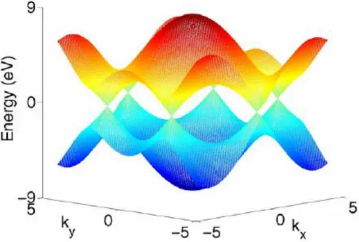
Figure 1.4.1 Electronic structure of graphene calculated basing on the tight-binding model with only orbitals concerned. Adapted from [11].
When the graphene sheet is rolled up to form a CNT, this orbital is still perpendicular to the nanotube surface and forms a delocalized network across the nanotube, which is responsible for the nanotube electronic properties. But the wave vector now is quantized in the circumferential direction [44]:
2 x x y y
9
where is the waver vector, is the chiral vector and x is an integer. As a result, CNT can be either metallic or semiconducting, depending on whether or not the allowed wave vectors by Eqn. 1.4.2 pass through any pair of the 6 graphene Fermi points, as illustrated in Fig. 1.4.2. Fig. 1.4.3 illustrates the examples of band structures for a semiconducting and a metallic zigzag CNTs. This leads to an equivalent condition for metallic CNT:
3
u v g, g is an integer. The theoretical linear conductance of a metallic CNT in low bias transport is given by [11]
2 4 1 6.5 Ω e G h k
, (1.4.3)
when the condition u v 3g is not satisfied, the CNT is semiconducting and the energy gap is given by [45]
2
d
cos 3α 0.4
(1 ) [1 ( 1) ] R pp p g d d V E R R
, (1.4.4)
Where Vpp is the tight-binding parameter for the orbital, Rd is the CNT radius divided by 0.142 nm, p is the reminder of
3
uv
10
Nanotubes are seldom in their perfect structures when measured in experiments. Interactions with metal contacts or substrate causes structural deformation and induce significant coupling, stretching and compression of bonds, all of which affect CNT’s electronic properties. Theoretically, the response of the change of band gap to a torsional stain is given in the following form [46]:
2 1 3
( ) gdE
sgn p tsin
d , (1.4.5)
where is the strain and t is the tight-binding overlap integral 2.77 eV. Clearly in Eqn. 1.4.5, the response is sensitive to the chiral structure of nanotubes.
11
Figure. 1.4.3 Illustration of the band structure of a semiconducting (left) and metallic zigzag CNTs. Adapted from reference [11].
1.5 Outline
12
13 1.6 References
[1] Iijima, S., Helical Microtubules of Graphitic Carbon. Nature354, 56-58 (1991). [2] Iijima, S. & Ichihashi, T., Single-Shell Carbon Nanotubes of 1-Nm Diameter.
Nature363, 603-605 (1993).
[3] Bethune, D. S., Kiang, C. H., Devries, M. S., Gorman, G., Savoy, R., Vazquez, J. & Beyers, R., Cobalt-Catalyzed Growth of Carbon Nanotubes with Single-Atomic-Layerwalls. Nature363, 605-607 (1993).
[4] Kreupl, F., Graham, A. P., Duesberg, G. S., Steinhogl, W., Liebau, M., Unger, E. & Honlein, W., Carbon Nanotubes in Interconnect Applications. Microelectron. Eng. 64, 399-408 (2002).
[5] Lu, J. P., Elastic Properties of Carbon Nanotubes and Nanoropes. Phys. Rev. Lett.
79, 1297-1300 (1997).
[6] Lu, J. P., Elastic Properties of Single and Multilayered Nanotubes. J. Phys. Chem. Solids58, 1649-1652 (1997).
[7] Qin, L.-C., Electron Diffraction from Carbon Nanotubes. Rep. Prog. Phys. 69, 2761-2821 (2006).
[8] Ngo, Q., Petranovic, D., Krishnan, S., Cassell, A. M., Ye, Q., Li, J., Meyyappan, M. & Yang, C. Y., Electron Transport through Metal-Multiwall Carbon Nanotube Interfaces. IEEE Trans. Nanotechnol.3, 311-317 (2004).
[9] Wei, B. Q., Vajtai, R. & Ajayan, P. M., Reliability and Current Carrying Capacity of Carbon Nanotubes. Appl. Phys. Lett.79, 1172-1174 (2001).
[10] Kis, A., Jensen, K., Aloni, S., Mickelson, W. & Zettl, A., Interlayer Forces and Ultralow Sliding Friction in Multiwalled Carbon Nanotubes. Phys. Rev. Lett.97 (2006). [11] Anantram, M. P. & Leonard, F., Physics of Carbon Nanotube Electronic Devices.
Rep. Prog. Phys.69, 507-561 (2006).
[12] Heinze, S., Tersoff, J., Martel, R., Derycke, V., Appenzeller, J. & Avouris, P., Carbon Nanotubes as Schottky Barrier Transistors. Phys. Rev. Lett.89 (2002).
[13] Javey, A., Guo, J., Wang, Q., Lundstrom, M. & Dai, H. J., Ballistic Carbon Nanotube Field-Effect Transistors. Nature424, 654-657 (2003).
14
[16] Babic, B., Furer, J., Sahoo, S., Farhangfar, S. & Schonenberger, C., Intrinsic Thermal Vibrations of Suspended Doubly Clamped Single-Wall Carbon Nanotubes.
Nano Lett.3, 1577-1580 (2003).
[17] Gao, R. P., Wang, Z. L., Bai, Z. G., de Heer, W. A., Dai, L. M. & Gao, M., Nanomechanics of Individual Carbon Nanotubes from Pyrolytically Grown Arrays. Phys. Rev. Lett.85, 622-625 (2000).
[18] Krishnan, A., Dujardin, E., Ebbesen, T. W., Yianilos, P. N. & Treacy, M. M. J., Young's Modulus of Single-Walled Nanotubes. Phys. Rev. B58, 14013-14019 (1998). [19] Poncharal, P., Wang, Z. L., Ugarte, D. & de Heer, W. A., Electrostatic Deflections and Electromechanical Resonances of Carbon Nanotubes. Science283, 1513-1516 (1999).
[20] Wong, E. W., Sheehan, P. E. & Lieber, C. M., Nanobeam Mechanics: Elasticity, Strength, and Toughness of Nanorods and Nanotubes. Science277, 1971-1975 (1997). [21] Hall, A. R., An, L., Liu, J., Vicci, L., Falvo, M. R., Superfine, R. & Washburn, S., Experimental Measurement of Single-Wall Carbon Nanotube Torsional Properties. Phys. Rev. Lett.96 (2006).
[22] Falvo, M. R., Clary, G. J., Taylor, R. M., Chi, V., Brooks, F. P., Washburn, S. & Superfine, R., Bending and Buckling of Carbon Nanotubes under Large Strain. Nature
389, 582-584 (1997).
[23] Gupta, S., Dharamvir, K. & Jindal, V. K., Elastic Moduli of Single-Walled Carbon Nanotubes and Their Ropes. Phys. Rev. B72 (2005).
[24] Tombler, T. W., Zhou, C. W., Alexseyev, L., Kong, J., Dai, H. J., Lei, L., Jayanthi, C. S., Tang, M. J. & Wu, S. Y., Reversible Electromechanical Characteristics of Carbon Nanotubes under Local-Probe Manipulation. Nature405, 769-772 (2000).
[25] Salvetat, J.-P., Briggs, G. A. D., Bonard, J.-M., Bacsa, R. R., Kulik, A. J., St, ouml, ckli, T., Burnham, N. A., Forr, oacute, L., aacute & szl, Elastic and Shear Moduli of Single-Walled Carbon Nanotube Ropes. Phys. Rev. Lett.82, 944 (1999).
[26] Ono, Y. & Ogino, T., Observation of Suspended Carbon Nanotube Configurations Using an Atomic Force Microscopy Tip. Jpn. J. Appl. Phys.48 (2009).
[27] Volodin, A., Van Haesendonck, C., Tarkiainen, R., Ahlskog, M., Fonseca, A. & Nagy, J. B., Afm Detection of the Mechanical Resonances of Coiled Carbon Nanotubes.
Appl. Phys. A-Mater. Sci. Process.72, S75-S78 (2001).
15
[29] Williams, P. A., Papadakis, S. J., Patel, A. M., Falvo, M. R., Washburn, S. & Superfine, R., Torsional Response and Stiffening of Individual Multiwalled Carbon Nanotubes. Phys. Rev. Lett.89 (2002).
[30] Meyer, J. C., Paillet, M. & Roth, S., Single-Molecule Torsional Pendulum.
Science309, 1539-1541 (2005).
[31] Demczyk, B. G., Wang, Y. M., Cumings, J., Hetman, M., Han, W., Zettl, A. & Ritchie, R. O., Direct Mechanical Measurement of the Tensile Strength and Elastic Modulus of Multiwalled Carbon Nanotubes. Mater. Sci. Eng. A-Struct. Mater. Prop. Microstruct. Process.334, 173-178 (2002).
[32] Charlier, J. C. & Michenaud, J. P., Energetics of Multilayered Carbon Tubules.
Phys. Rev. Lett.70, 1858-1861 (1993).
[33] Kolmogorov, A. N. & Crespi, V. H., Smoothest Bearings: Interlayer Sliding in Multiwalled Carbon Nanotubes. Phys. Rev. Lett.85, 4727-4730 (2000).
[34] Saito, Y., Fullerenes: Recent Advances in the Chemistry and Physics of Fullerenes and Related Materials (1994).
[35] Zhao, Y., Ma, C. C., Chen, G. H. & Jiang, Q., Energy Dissipation Mechanisms in Carbon Nanotube Oscillators. Phys. Rev. Lett.91 (2003).
[36] Servantie, J. & Gaspard, P., Methods of Calculation of a Friction Coefficient: Application to Nanotubes. Phys. Rev. Lett.91 (2003).
[37] Legoas, S. B., Coluci, V. R., Braga, S. F., Coura, P. Z., Dantas, S. O. & Galvao, D. S., Molecular-Dynamics Simulations of Carbon Nanotubes as Gigahertz Oscillators. Phys. Rev. Lett.90 (2003).
[38] Yakobson, B. I., Brabec, C. J. & Bernholc, J., Nanomechanics of Carbon Tubes: Instabilities Beyond Linear Response. Phys. Rev. Lett. 76, 2511-2514 (1996).
[39] Guo, W. L., Zhong, W. Y., Dai, Y. T. & Li, S. A., Coupled Defect-Size Effects on Interlayer Friction in Multiwalled Carbon Nanotubes. Phys. Rev. B72 (2005).
[40] Cumings, J. & Zettl, A., Low-Friction Nanoscale Linear Bearing Realized from Multiwall Carbon Nanotubes. Science289, 602-604 (2000).
[41] Bourlon, B., Glattli, D. C., Miko, C., Forro, L. & Bachtold, A., Carbon Nanotube Based Bearing for Rotational Motions. Nano Lett.4, 709-712 (2004).
16
[43] Craighead, H. G., Nanoelectromechanical Systems. Science 290, 1532-1535 (2000).
[44] Deniz, H., Electron Diffraction and Microscopy Study of Nanotubes and Nanowires. PhD Thesis, The University of North Carolina at Chapel Hill, (2007).
[45] Yorikawa, H. & Muramatsu, S., Energy Gaps of Semiconducting Nanotubules.
Phys. Rev. B52, 2723-2727 (1995).
Chapter 2
Characterization Techniques for Carbon
Nanotubes
18 2.1 Scanning Tunneling Microscopy (STM)
Scanning tunneling microscope is a non-optical surface imaging instrument with atomic precision invented in 1981. The invention won its inventors Gerd Binning and Heinrich Rohrer, the Nobel Prize in Physics in 1986. A STM can have a lateral resolution of 0.1 nm and a depth resolution of 0.01 nm. Within such a high resolution, the outermost atoms on surface can be routinely imaged.
The working principle and high resolution capability of STM are based on the concept of quantum tunneling. When the metal probe of a STM is brought very close to sample surface (usually about
o
4 7 A ) with a voltage bias applied between the probe tip and surface, electrons will tunnel through the vacuum between them and form a tunneling current. This current is a function of the separation distance between tip and surface, bias voltage, tip radius and local density of states of the surface. Morphological information is acquired through monitoring the tunneling current when the probe is scanning across the surface. The local density of states can be derived from the differential conductance calculated from tunneling current and bias voltage curve. The surface morphology thus can be reconstructed based on the local density of states.
19
estimating the line profiles perpendicular to the tube axial direction. An accuracy of 1
in helical angle and 0.1 nm in diameter measurement can be obtained and this allows for an identification of the chiral structure. Besides the atomic structure of a SWNT, the SWNT’s band gap can also be derived from the conductance calculated from an I-V curve measured by STM.
20
Figure 2.1.1 Atomically resolved STM image of an individual SWNT. T, H and are the tube axis, zigzag direction and helical angle, respectively. The lattice of black dots represents the centers of the hexagons. Adapted from reference [1].
2.2 Raman Spectroscopy
Raman spectroscopy is a widely used technique for the study of vibrational, rotational, and other low frequency modes in materials. The basic principle of Raman spectroscopy is the concept of Raman scattering of monochromatic light which is usually comes from lasers in the visible, near infrared and near ultraviolet range. The interactions between photons of the laser and molecular vibrations, phonons or other excitation modes in the system will shift the laser photons’ energy up and down. The information about phonon modes in the system can be obtained from this energy shift.
21
diameters of the nanotubes but not their helicities. The peaks are located between 120
-1
cm and 350 -1
cm , respectively. The frequency of RBM mode is usually used to determine the diameter of a SWNT and is given by
RBM
A
w B
d
(2.2.1)
where d is tube diameter, A (unit: -1
cm nm) and B (unit: -1
cm ) are constants and vary
between individual SWNT and SWNT bundles. A and B have been found to be 248
-1
cm nm and 0 -1
cm for isolated SWNTs on Si/SiO2 substrate [9].
The diameter alone is not enough to identify the chirality of a SWNT. The second parameter needed is the transition energies of inter-bands which can be obtained from resonant Raman scattering (RRS). A plot of transition energies of all chiral structures calculated from tight-binding model should be compared with those obtained from RRS experiments. With the tube diameter, the chiral indices can be determined by a match between theoretical and measured transition energies [10].
22 2.3 Optical Absorption Spectroscopy
Optical absorption spectroscopy refers to the technique which measures the absorption spectrum of a material when the material is exposed to light (usually the light source covers a broad swath of wavelengths from infrared to ultraviolet). If the incident wavelength matches certain transition energy, the photon will be absorbed and the material will transit to an excited state. Emission occurs a photon with energy equal to the energy difference between the ground state and excited state. Therefore, the absorption spectrum of a material can be calculated from its emission spectrum using appropriate theoretical models and additional information about the quantum mechanical states of the substance. The inter-band transition energies and electronic structure of SWNTs can be studied by optical absorption spectroscopy based on the principle mentioned above. In an optical absorption spectroscopy measurement, SWNTs are usually well dispersed in a solution and show high energy-resolution in their optical absorption spectrum. The method to indentify the chiral indices of SWNTs is similar to that of Raman spectroscopy mentioned in last section [13-16].
The disadvantage of optical absorption spectroscopy is that it is hard to characterize the structure of a MWNT. It is also difficult to identify the structure of a single SWNT because of the weak signal.
2.4 Transmission Electron Microscopy and Electron Diffraction
23
Scattered electrons are focused to form a magnified image onto an imaging device such as a fluorescent screen, a photographic film, or a sensor such as a CCD camera. The physical principles behind the development of TEM should be attributed to the following two aspects: (1) the wave-like characteristics of electrons first postulated by Louis de Broglie in 1925 [17]; (2) the discovery of electron focusing lenses which use electromagnetic field to focus moving electrons in desired direction by Hans Busch in 1926 [18]. The first transmission electron microscope was built by Ernst Ruska and Max Knoll in 1932 [19]. Ernst Ruska shared the Nobel Prize in Physics with Gerald Binning and Hans Rohrer in 1986. The wavelength of an electron accelerated by a voltage between 100 kV to 400 kV is about two orders magnitude smaller than the size of an atom which has a diameter of about 0.1 nm. In principle, it is possible to resolve material structure well below the atomic level according to the Raylaigh criteria [20]. However, a TEM with this resolution limit is impossible to construct due to the imperfections of the magnetic lenses. Nowadays, a good TEM can achieve the resolution on the order of 0.1 nm. In contrast, electron diffraction is much less sensitive to the imperfections of magnetic lenses, but more dependent on the convergence of incident electrons [21].
Within this research, CNT images and electron diffraction patterns are taken on JEM 2010F FasTEM electron microscope (vender JEOL). All the diffraction patterns are taken by the nanobeam electron diffraction method with beam waist of about 80 nm.
2.4.1 Theory of Electron Imaging in TEM
24
an image on the image plane. Two imaging mechanisms are usually used: amplitude contrast and phase contrast [22]. In the amplitude contrast mode, the image contrast is the result from the electrons scattered in different angles within a specimen. The areas of the specimen with higher mass or larger Coulomb potential will scatter more electrons toward large angular regions which are away from optical axis. If a small aperture is used, most electrons which are scattered in large angles can be excluded except the selected beam. As a result, the areas corresponding to the higher mass or strong atomic potential positions within the specimen will turn dark in the image. On the other hand, image contrast in the phase contrast mode comes from the phase difference of electrons caused by interactions between electrons and the Coulomb potential of the specimen. A large objective aperture is usually used to allow more scattered beams to pass through the objective lenses to form an image. It offers a much higher structural resolution and is usually called high resolution TEM compared to the amplitude contrast mode. But it requires that the specimen be thin.
Like the image formation in an optical microscope, the scattered electron waves in the diffraction plane will form a two-dimensional structure image projected from three-dimensional specimen on the image plane. However, in order to better interpret the electron imaging process, both non-linear imaging and dynamical electron diffraction effects need to be considered [23].
25 ( , ) e px p( , )
o x y iV x y
, (2.4.1) where
/ ( U) is the relativistic interaction constant with U being the accelerating voltage applied on electrons, V x yp( , ) is the projected Coulomb potential of specimen in a plane perpendicular to the direction of the incident electron beam and is the wave length of the electrons. For a thin specimen constituted of light atoms, the weak phase object approximation can be applied and Eqn. 2.4.1 can be simplified to( , ) 1 ( , ) o x y i V x y
, (2.4.2)
where the unit 1 represents the transmitted wave which has no interaction with the specimen and the imaginary part corresponds to the scattered waves. The image wave on the image plane is a convolution between the object wave and a contrast transfer function
:
( ) ( ) ( )
i r o r T r
, (2.4.3)
where is the convolution operator. The convolution operation of two functions can be expressed as the product of their corresponding Fourier transforms in the reciprocal space:
( ) ( ) ( )
i q o q T q
. (2.4.4)
The contrast function in a TEM includes the information of aperture function, spherical aberration and imperfection of focusing of the objective lens and is given by [25]
( ) ( )exp[2 ( )]
T q a q
i q , (2.4.5) where a q( ) is the aperture function of the objective lens and4 2
1 1
( )
4 s 2
q C q fq
26
where Cs and Δf are the spherical aberration coefficient and defocus of the objective lens, respectively. Using Eqn. 2.4.5 and 2.4.6, Eqn. 2.4.3 can then be expressed as
( , ) 1 ( , ) [ ( , )] ( , ) [ ( , )]
i x y V x yp Im T x y i V x yp Im T x y
. (2.4.7)
In weak phase object approximation, Vp 1, the image intensity can then be further simplified into
2 i
( , ) | Ψ( , )| 1 2 p( , ) [ ( , )]
I x y x y V x y Im T x y . (2.4.8) Eqn. 2.4.8 shows that only the imaginary part of the contrast transfer function contributes to the image intensity in the weak phase object approximation and linear imaging.
2.4.2 TEM Imaging of CNT
Because CNTs are formed by graphene layers and carbon atoms have a low atomic number ( ), the weak phase object approximation discussed in the last section can be used to interpret the TEM images of carbon nanotubes structure (an image actually corresponds to the projected Coulomb potential of the CNT [26]). A high resolution TEM equipped with a field emission electron gun can easily obtain structural images of a CNT with a resolution of about 0.2 nm. Thermal and mechanical vibrations, stage drift, and instabilities of the magnetic lenses will compromise the quality and the resolution of a TEM image.
27
measured from a line profile perpendicular to the tube axis. But the measurement needs to be very careful because the position and width of the dark line are very sensitive to the imaging condition such as the defocus of the objective lens. It also causes errors in the diameter measurement if the nanotube is not oriented within a horizontal plane, i.e. not perpendicular to incident beam. The error becomes more significant when measuring the smaller diameter tube due to the pronounced curvature [27].
Figure 2.4.1 TEM images of (a) SWNT, (b) DWNT, and (c) 6-wall carbon nanotube taken with JEM 2010F operated at 80 kV.
2.5 Electron Diffraction Theory of Carbon Nanotube
28
from the diffraction pattern of graphene. Since carbon nanotubes are formed from graphene, they share some features in the diffraction patterns: diffraction layer lines resulting from the honeycomb lattice of graphite have a well-defined periodicity in the tube axial direction. But the structure in the radial direction is not periodic in a CNT when the graphene is rolled along the chiral vector to form a nanotube. As a result, the reflections are sharply defined along tube axis but elongated perpendicular to the tube axis.
A complete CNT electron diffraction theory was formulated by Qin in 1994 [28] and Lucas et al. in 1996 [29, 30] based on the kinematical theory of scattering from helical structure developed by Cochran, Crick and Vand in 1952 [31]. The theory has been proved to be powerful in characterization of carbon nanotube’s chiral structure. The atomic scattering amplitude for electrons incident on atoms are described by the first Born approximation [30]
2
2
( ) exp 2
me
F q v r iq r dr
h
, (2.5.1)where v r( ) is the Coulomb potential of the scattering atom, e is the charge of an electron, is the relativistic mass of electron, is Plank’s constant and is the scattering vector with the magnitude defined as
2sin(Θ / 2)
q
, (2.5.2)
where Θ is the total scattering angle and is the wave length of the incident electron. The diffraction intensity distribution I q( ) in reciprocal space is the square of the scattering amplitude
2| ( ) |
29
Since the atoms of a CNT are periodically located on a pair of helices about the tubular axis, we start the derivation of diffraction patterns from the scattering amplitude of a continuous helix, which is expressed in the cylindrical coordinates for the convenience:
1
1
( , , ) exp[ ( )]
2 n
F R l z in c
20 0 0
2 ( , , ) (2 ) exp[ ( )]
c
n
lz
V r z J rR i n rdrd dz
c
(2.5.4)where ( , Φ, )R l are the cylindrical coordinates in reciprocal space, ( , , )r
z are the cylindrical coordinates in real space, Jn is the n-th order Bessel function, c is the periodicity in the tube axis, and V r( , , )z 2 me2 v r( )h
is the modified scattering potential.
When the atoms are located on a helix with a radius of ro and a pitch length C, the modified scattering potential has the following form
2
( , , ) o ( o) ( z )
V r z V r r
C
. (2.5.5) Using Eqn 2.5.5, the scattering amplitude can be expressed as
, (2.5.6)
For a SWNT, carbon atoms are only located on discrete points of the helix with radius r0, shown in Fig. 2.4.1, the structure factor become
0
2 π
( , Φ, ) exp[in(Φ )] (2 ) exp[ ( )]
2
j
n j j
n j
lz
F R l J r R f i n
c
30
where (j,zj) are the coordinates of carbon atoms, fjis the atomic scattering amplitude
of carbon, summation is done over atoms in an asymmetric cell and n over all integers which are allowed by selection rule (
Δ
l n m
c C ) discussed later.
Since carbon atoms can be treated as discrete points with an equally spacing on a continuous helix, as shown in Fig 2.5.1 [26]. The scattering potential of carbon atoms can be regarded as the product of a continuous helix and these equally spacing points. The diffraction pattern in reciprocal space is then convolution of the structure factor of the helix and that of the equally spacing points. This gives the allowed reflections on the diffraction layer line through the following selection rule:
Δ
l n m
c C , (2.5.8)
where l is the coordinate for F R( , Φ, )l , c is the new structural periodicity in the axial direction of a single helix in a SWNT, and m is an integer. For a SWNT with chiral indices (u, v), we have perimeterAa uo( 2 v2 uv)1/2, pitch length CAtan(60 ), helical angle arctan 3
2
v
v u
and the distance between atoms aosin(60 )
.
The axial periodicity is given by c 3Ch /Mwhere M is the maximum common divisor of (2u+v) and (u+2v). By using these relations, we can rewrite the Eqn. 2.5.8 as
2 2
( ) ( ) /
31
32
Meanwhile, the positions of carbon atoms in a SWNT can be expressed in cylindrical coordinates in the following equation
1,0 0 1,0 0 (30 )
0,1, 2,..., 1 (30 )
j
j
x ja cos
j v
z ja sin
(2.5.10)
and
1,1 1,0 0
0
1,1 1,0 0
0
(30 ) 3
0,1, 2,..., 1 (30 )
3
j j
j j
a
x x ja cos
j v
a
z z ja sin
. (2.5.11)
Plugging Eqn. 2.5.10 and 2.5.11 into Eqn. 2.5.7, we can have the structure factor expressed as
,
, Φ, , ( , ) exp Φ 2
uv uv uv n
n m
F R l f n m n m J dR in
, (2.5.12)where
,
1 exp 2
2
3uv
n u v m
n m i
v
and
1 exp 2 ,
1 exp 2 uv
i n u v m n m
u v m i n v .
From the above expression, the structure factor can be divided into two parts: (1) reflections of graphene lattice, which is described as
,
, ( , )
uv uv
n m
n m n m
; (2) curvature effects from the cylindrical structure described as
,
exp[ Φ ] 2
n n m
J dR in
.The intensity distribution of diffraction pattern is obtained by
2
| ( , Φ, ) | uv
33
The intensity distribution on each allowed diffraction layer is governed by Bessel functions with different orders. But only one specific Bessel function will be dominant in the intensity distribution while the contribution from other Bessel functions are insignificant [24]. This feature actually results in great convenience in the experiment for the determination of the chiral indices of a CNT.
Fig. 2.5.2 is a simulated diffraction pattern of a SWNT [32]. The three primary layer lines l l1, 2 and l3, are the most significant diffraction layer lines. They are formed by the (10) ,(10)and (11) reflections of graphene. The two hexagons indicate the primary Bragg reflections from the top and the bottom surfaces of the carbon nanotube, giving six primary diffraction layer lines on the diffraction pattern. The elongation of the diffraction spots perpendicular to the tubule axis is due to a lack of translational periodicity in this direction. As we can see from the image, the peak of intensity is shifted because of the curvature of the carbon nanotube.
The scattering intensity on the equatorial layer line ( is dominated by Bessel function of order 0 and the intensity is proportional to the square of the zero order Bessel function J0 . The three primary layer lines, l l1, 2 and l3 have the values
1 (2 ) /
l uv M , l2(u2 ) /v M and l3 (u v ) /M , respectively. By using the selection rule, Eqn. 2.5.9, together with the value of l l1, 2 and l3, the order of dominant Bessel function of the three layer lines are solved out to be n1 v , n2 u and
3 ( )
n u v , respectively. Therefore, the intensities of the 3 primary diffraction layer lines are
2 1
( , , ) | v( ) |
34
22
, Φ, | u( ) |
I R l J dR , (2.5.15)
23
, Φ, | u v( ) |
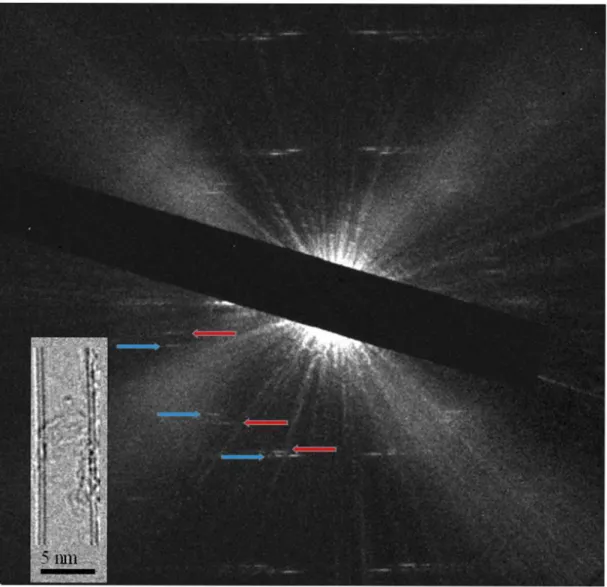
I R l J dR . (2.5.16) Eqn. 2.5.14, 2.5.15 and 2.5.16 provide a way to identify the chiral indices of a SWNT accurately and unambiguously by electron diffraction. Since intensities of the layer line l1 and l2 are dominated by the Bessel functions of order v and u, respectively, the order of the Bessel function can be derived from the ratio of the first two peak positions which can be measured directly on the diffraction layer lines. Fig. 2.5.3(a) is the electron diffraction pattern of the SWNT (17, 2) together with the TEM image (inset) of the nanotube. The chiral indices (17,2) are derived from the ratio of first two peak positions, 1
2
X
X measured on the intensity profiles of the layer lines and as illustrated
in the Fig. 2.5.3(b) and (c), respectively.
The layer line spacings provide another way to identify the chiral indices of a CNT. As shown in Fig. 2.5.2, the line spacing and can be expressed
* 1 * 2 (90 ) (30 )
D a sin
D a sin
(2.5.17)
where a* is basis vector of the graphene lattice in reciprocal space. Thus, the helical angle can be rewritten as
2 1 1 2 tan( ) 3 D D D
, (2.5.18)
Combining the Eqn. 1.2.5 and 2.5.18, the ratio of chiral indices are deduced into
2 1 1 2 2 2 D D v
u D D
35
Once the ratio of the chiral indices is obtained from the layer line spacings, the chiral indices can be usually determined unambiguously with supplementary information of tube diameter which can be directly measured from TEM images.
36
37
38
39 2.6 References
[1] Wildoer, J. W. G., Venema, L. C., Rinzler, A. G., Smalley, R. E. & Dekker, C., Electronic Structure of Atomically Resolved Carbon Nanotubes. Nature391, 59-62 (1998).
[2] Odom, T. W., Huang, J. L., Kim, P. & Lieber, C. M., Atomic Structure and Electronic Properties of Single-Walled Carbon Nanotubes. Nature391, 62-64 (1998). [3] Hassanien, A., Tokumoto, M., Kumazawa, Y., Kataura, H., Maniwa, Y., Suzuki, S. & Achiba, Y., Atomic Structure and Electronic Properties of Single-Wall Carbon Nanotubes Probed by Scanning Tunneling Microscope at Room Temperature. Appl. Phys. Lett.73, 3839-3841 (1998).
[4] Hertel, T., Walkup, R. E. & Avouris, P., Deformation of Carbon Nanotubes by Surface Van Der Waals Forces. Phys. Rev. B58, 13870-13873 (1998).
[5] Wong, E. W., Sheehan, P. E. & Lieber, C. M., Nanobeam Mechanics: Elasticity, Strength, and Toughness of Nanorods and Nanotubes. Science277, 1971-1975 (1997). [6] Rubio, A., Spectroscopic Properties and Stm Images of Carbon Nanotubes. Appl. Phys. A-Mater. Sci. Process.68, 275-282 (1999).
[7] Giusca, C. E., Tison, Y., Stolojan, V., Borowiak-Palen, E. & Silva, S. R. P., Inner-Tube Chirality Determination for Double-Walled Carbon Nanotubes by Scanning Tunneling Microscopy. Nano Lett.7, 1232-1239 (2007).
[8] Dresselhaus, M. S., Dresselhaus, G., Saito, R. & Jorio, A., Raman Spectroscopy of Carbon Nanotubes. Phys. Rep.-Rev. Sec. Phys. Lett.409, 47-99 (2005).
[9] Jorio, A., Saito, R., Hafner, J. H., Lieber, C. M., Hunter, M., McClure, T., Dresselhaus, G. & Dresselhaus, M. S., Structural (N, M) Determination of Isolated Single-Wall Carbon Nanotubes by Resonant Raman Scattering. Phys. Rev. Lett.86, 1118-1121 (2001).
[10] Telg, H., Maultzsch, J., Reich, S., Hennrich, F. & Thomsen, C., Chirality Distribution and Transition Energies of Carbon Nanotubes (Vol 93, Art No 177401, 2004). Phys. Rev. Lett.93 (2004).
[11] Benoit, J. M., Buisson, J. P., Chauvet, O., Godon, C. & Lefrant, S.,
Low-Frequency Raman Studies of Multiwalled Carbon Nanotubes: Experiments and Theory.
Phys. Rev. B66 (2002).
40
[13] Lian, Y. F., Maeda, Y., Wakahara, T., Akasaka, T., Kazaoui, S., Minami, N., Choi, N. & Tokumoto, H., Assignment of the Fine Structure in the Optical Absorption Spectra of Soluble Single-Walled Carbon Nanotubes. Journal of Physical Chemistry B107, 12082-12087 (2003).
[14] Liu, X., Pichler, T., Knupfer, M., Golden, M. S., Fink, J., Kataura, H. & Achiba, Y., Detailed Analysis of the Mean Diameter and Diameter Distribution of Single-Wall Carbon Nanotubes from Their Optical Response. Phys. Rev. B66 (2002).
[15] Kataura, H., Kumazawa, Y., Maniwa, Y., Umezu, I., Suzuki, S., Ohtsuka, Y. & Achiba, Y., Optical Properties of Single-Wall Carbon Nanotubes. Synth. Met.103, 2555-2558 (1999).
[16] Jost, O., Gorbunov, A. A., Pompe, W., Pichler, T., Friedlein, R., Knupfer, M., Reibold, M., Bauer, H. D., Dunsch, L., Golden, M. S. & Fink, J., Diameter Grouping in Bulk Samples of Single-Walled Carbon Nanotubes from Optical Absorption
Spectroscopy. Appl. Phys. Lett.75, 2217-2219 (1999).
[17] Broglie, L. D., Research on the Theory of Quanta. Ann. De Physiques3, 107 (1925).
[18] Busch, H., On the Modes of Action of the Concentrating Coil in the Braun Tube.
Arch. Electrotechnik18, 12 (1927).
[19] Knoll, M. & Ruska, E., The Electron Microscope. Physik78, 22 (1932). [20] Born, M. & Wolf, E., Principles of Optics 1964).
[21] Joy, D. C., Romig, A. D. & Goldstein, J., Principles of Analytical Electron
Microscopy (Plenum Press, New York, 1986).
[22] Deniz, H., Electron Diffraction and Microscopy Study of Nanotubes and Nanowires. PhD Thesis, The University of North Carolina at Chapel Hill, (2007).
[23] Cowley, J. M., Diffraction Physics (North-Holland Pub. Co. ; Sole distributors for the U.S.A. and Canada, Elsevier North-Holland, Amsterdam; New York; New York, 1981).
41
[27] Qin, C. & Peng, L. M., Measurement Accuracy of the Diameter of a Carbon Nanotube from Tem Images. Phys. Rev. B65 (2002).
[28] Qin, L.-C., Electron-Diffraction from Cylindrical Nanotubes. J. Mater. Res.9, 2450-2456 (1994).
[29] Lambin, P. & Lucas, A. A., Quantitative Theory of Diffraction by Carbon Nanotubes. Phys. Rev. B56, 3571-3574 (1997).
[30] Lucas, A. A., Bruyninckx, V. & Lambin, P., Calculating the Diffraction of Electrons or X-Rays by Carbon Nanotubes. Europhys. Lett.35, 355-360 (1996). [31] Cochran, W., Citation-Classic - the Structure of Synthetic Polypeptides .1. The Transform of Atoms on a Helix. Current Contents/Physical Chemical & Earth Sciences, 16-16 (1987).
Chapter 3
Experimental Techniques
3.1 Introduction
43 3.2 Carbon Nanotube Deposition
Since the discovery of CNT [1], there have been three major methods to grow SWNTs or MWNTs: (a) arc-discharge evaporation of graphite [1-5]; (b) laser ablation of graphite [6-9]; and (c) chemical vapor deposition [10-20]. They will only be discussed briefly here to explain the reason why chemical vapor deposition is chosen for my devices.
In an arc-discharge synthesis, a DC or AC voltage is applied between two graphite electrodes which are separated by about 1 mm to create discharge plasma. The material on the anode is evaporated by high temperature plasma and is condensed on the cathode. Carbon nanotubes are found in the deposits on the cathode. When transition metals are present in the anode serving as catalysts, SWNTs can be synthesized on the cathode. Otherwise, only MWNTs are produced in the deposits [2].
In the laser ablation method, a solid carbon target is placed in a quartz tube at high temperature. A pulsed laser is used to blast and to evaporate the carbon target. The products are found to be 90% pure CNT. If the target contains transition metal catalysts such as Rh/Pd and Ni/Co [6, 7], SWNT can be synthesized. Otherwise, products only contain MWNTs.
44
can change the polarity of the MWNTs and makes the MWNTs easily to disperse on the substrate from the solution. The substrate is ready for further fabrication after it is dried under nitrogen flow.
The dispersion of individual SWNTs or DWNTs on substrate is more challenging than MWNTs by the above method due to nanotube bundling, resulted from their low mass-to-surface area ratio. Surfactants or organic polymers are usually added into the nanotube solution to debundle carbon nanotubes by attaching positive or negative chemical molecules on the surface of nanotubes to overcome the attractive van der Waals force within the nanotube bundles [21, 22]. These suffactants can be removed later from nanotubes by changing solvent or by smooth oxidation. The result is good for dispersing CNTs on carbon grids for TEM imaging, but is far from being satisfied for dispersing individual CNTs uniformly on silicon substrate at a low concentration. The device fabrication requires a CNT density of about 5 nanotubes per one hundred square micrometers on the substrate. Thus, dispersion by liquid solution requires a CNT solution with a very low concentration. However, effects of surfactants in such a low concentration solution are not good and the individual CNT deposition is often not certain. Furthermore, the removal of surfactants by oxidation can very easily burn nanotubes or results in structural defects, especially when the number of nanotubes is small.
45
at high temperature. When passing through the quartz tube, organic gases are thermally decomposed and carbon nanotubes grow on the catalysts. It requires the catalyst particles, which usually contain Fe or Ni nano-particles, be of very small diameter (<10 nm). Since the nanotubes are grown on the catalysts, the density of CNT on the substrate can be precisely controlled by the catalyst density dispersed on the substrate.
3.3 CNT Synthesis by Chemical Vapor Deposition
The CNTs in our experiment are grown by chemical vapor deposition. Different catalysts, silicon based substrates and growth methods guided by Dr Jie Liu’s group in Duke University have been tried to achieve the required CNT deposition density on the device substrates [16-20, 23].
Fe/Mo nano-particles are first used as the catalysts for SWNT synthesis in the CVD system. The catalysts are diluted into 1:100000 in hexane and then dispersed onto the silicon substrate. The substrates are annealed in air at 700 Cfor 10 minutes and then feeding gases consisting of methane, ethylene and hydrogen are purged through at
46
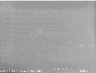
Figure 3.3.1 SEM image of SWNTs using Fe/Mo nano-particles as catalysts.
47
Figure 3.3.2 SEM images of SWNTs using quartz wafer as the substrate and iron chloride as catalysts.
48
In order to grow long nanotubes and reach the required SWNT/DWNT density on the silicon substrate, the following method is finally chosen in our experiments (the details of the growth method are discussed in Appendix I) [18]. For a DWNT growth,
2
49
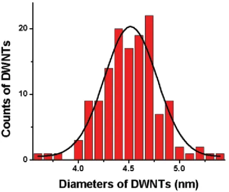
Figure 3.2.5 Diameter distribution of DWNT grown by chemical vapor deposition directly onto a substrate. The image is adapted from [18].
50
3.4 Nano-Electromechanical Device Based on a Suspended CNT
Two types of CNT devices are used in this thesis to study the correlations between the nanotube properties and its chiral structure. In the first type of device, a single carbon nanotube is suspended in air between two or four anchoring electrodes which are used to measure the electrical resistance of the CNT. In the second type of device, a single carbon nanotube, which is suspended between two anchoring electrodes, works as a torional bearing attached with a metal anchor. An external electric field is applied via a side gate to actuate the metal paddle and thus to twist the nanotube, as illustrated in Fig. 3.3.1. The torsional strains and the corresponding electromechanical response of the CNT can be measured simultaneously on this type of device. The details of device fabrication will be described in Appendix II. Due to the similarities between two types of devices, this section focuses on a brief description of the fabrication of the second type device.
51
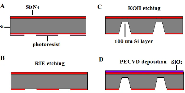
Figure 3.3.1 Schematic of CNT torsional device. A metal paddle is suspended on an individual CNT which is held by two metal anchors across an opening etched on a membrane consisting of 300 nm silicon dioxide and 300 nm silicon nitride. A side gate is placed aside to actuate the metal paddle by an applied voltage.
(2) The silicon nitride layer on top of which the photoresist has been removed is etched away in a reactive ion etching (RIE) process, as illustrated in Fig. 3.3.2(B). The sample is placed in the RIE chamber at an atmosphere of C F3 8and O2 gases. Chemically reactive plasma are induced in the chamber by an electromagnetic field to etch the exposed silicon nitride layer. The rest of the wafer is protected from etching by photoresist. The photoresist is removed by sonication in acetone for 30 seconds after etching.
52
etchant and etches the silicon (100) with an angle of 54.74° from the plane at a speed about 1 μm per minute. The silicon nitride layers coated on both sides of the wafer work as a KOH stopper to protect the silicon beneath from etching. Only the areas on top of which the nitride layer is etched away by RIE in the last step are exposed to KOH. The etching process is stopped when the etching depth reaches 400 μm, leaving a 100 μm silicon layer which works as a support to protect the underlying nitride layer from breaking in future sonication. The entire process is supervised in an optical microscope in case the sample is over-etched.
(4) A 50 nm silicon nitride layer and a 300 nm silicon dioxide layer are deposited onto the top surface of the sample by plasma enhance chemical vapor deposition (PECVD), Fig. 3.3.2(D). Although silicon nitride is a good etchant stopper in KOH solution, the defects on the nitride layer will be enlarged and thus the local nitride will be etched through by KOH in a long time etching process (usually about several hours). This effect results in pin holes (on the micrometer order) on the surface. As the result, circuit fabricated on the surface will be short to the substrate if metal happens to be deposited on these pin holes. Therefore, a 50 nm PECVD silicon nitride layer is first coated on the wafer surface to block these pin holes. Another 300 nm silicon dioxide layer is deposited onto the substrate for CNT growth.
53
Figure 3.3.2 Schematic of the first 4 steps of device fabrication. (A) Photolithography is performed on the backside of the wafer. The photoresist protects the covered area from RIE etching. (B) RIE etching is applied to etch the silicon nitride without the protection of photoresisit. (C) The sample is dipped in 15% KOH solution for silicon etching. Etching is stopped when the etching depth reaches 400 μm. 100 μm silion layer is left as a support for the silicon nitride layer. (D) A 40 nm silicon nitride film and 300 nm dioxide film is deposited onto the top surface of the wafer by PECVD.
54
macroscopic electrodes that decrease in size to an 80 μm × 80 μm area where devices are to be fabricated, marked by the circle as illustrated in Fig. 3.3.3[24].
Figure 3.3.3 Schematic of the macroscopic electrodes deposited onto a wafer by photolithography. The schematic is not drawn to scale for illustration purpose. Adapted from [24].
(7) CNTs are broken apart by applying a large current (tens of micro amperes) between the neighboring electrodes if the CNTs are bridging multiple leads as illustrated in Fig. 3.3.4(A) and (B). The large amount of heat generated as a large current (about
10 40 μA ) passing through CNTs causes the oxidation of carbon atoms and thus breaks the nanotubes. As the result, the applied current will become immeasurable once the nanotube is broken.
55
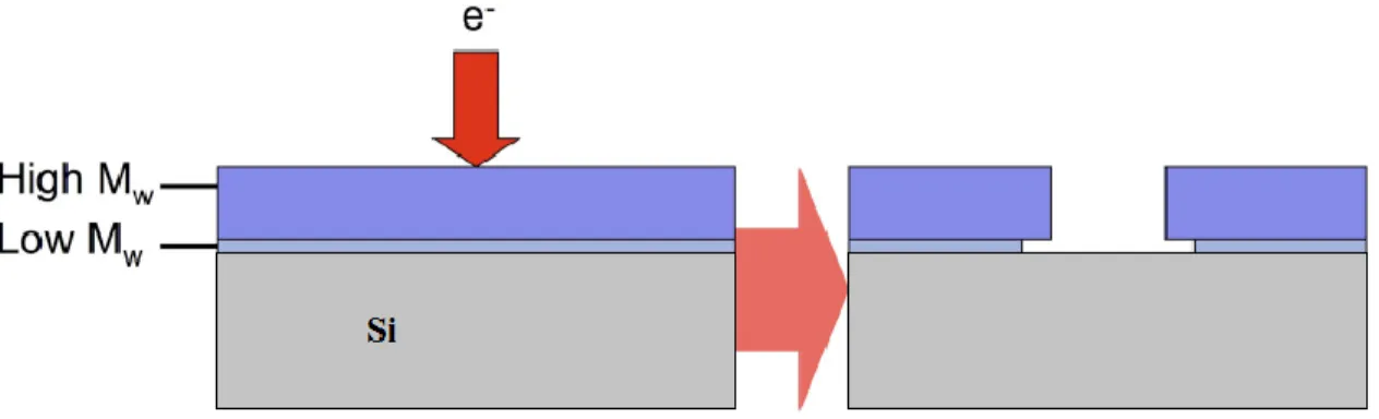
electron beam lithography is very similar to that of photolithography, except that the photoresist is replaced by electron beam resist poly methyl methacrylate (PMMA) here. A low molecular weight (M=350 K) PMMA is spin-coated on the sample at the spin speed of 5000 rpm, and then subject to a soft bake (180 ℃) for 2 minutes on a hot plate. A second layer PMMA (M=996K) is spin-coated on the sample at the spin speed of 4000 rpm, and then subject to a 2 hours bake (180 ) in a furnace to remove the solvent. After exposed to electron beam, the sample is soaked in developer (mixture of methyl isobutyl ketone and isoproponal at the ratio of 1: 3) to remove the exposed PMMA. Thermal evaporation is followed to deposit 10 nm Cr and 80 nm Au onto the sample surface. The metal atop the undeveloped PMMA is removed by acetone soak, leaving the substrate-bound areas only where exposure occurred. Double PMMA layers are used to help metal peel off in acetone soak. Since the lighter PMMA is more sensitive to electron beam than the heavier PMMA, it will be de-crosslinked more under the same electron dose and give an undercutting gutter after lithography, as illustrated in Fig. 3.3.5. Such a shape makes the metal atop the PMMA more easily to peel off when the underlying PMMA is dissolved in acetone.
56
Figure 3.3.4 (A) SEM image of the device area before electron beam lithography. The CNTs marked by black circle bridge the neighboring electrodes and are broken by applying a large electric current. (B) The nanotubes are broken after a large current oxidizes the carbon atoms. The inset is an enlarged SEM image where the CNT is broken point. (C) SEM image of the device after metal paddles and anchors are patterned. (D) An enlarged SEM device image of the area marked by the rectangle in (C).
57
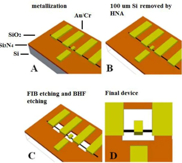
(10) Focused ion beam (FIB) is used to etch away the silicon nitride layer right below the CNT device as illustrated in Fig. 3.3.6(C). A cross fiduciary mark used as alignment mark is first etched through on the front side of the device. Then, the device is flipped 180 and the positions of CNT devices on the membrane are located according to the fiduciary mark. Windows with a size of 1.2 μm×1.8 μm are etched on these positions, leaving a 300 nm silicon dioxide layer to support the devices.
(11) Buffered hydrofluoric acid (BHF) is used to etch the 300 nm silicon dioxide layer which is left in the last step to fully suspend the nanotube and the paddle on the tube as illustrated in Fig. 3.3.6(C). PMMA (M=996 K) is first spin-coated onto the sample surface, working as a BHF stopper. Another electron beam lithography is then performed on the sample to open a 0.4 μm×0.8 μm etching window on the device, leaving the rest of sample protected by PMMA from BHF. A drop of BHF is placed onto the device for 5 minutes to etch away the silicon dioxide layer.
58
59
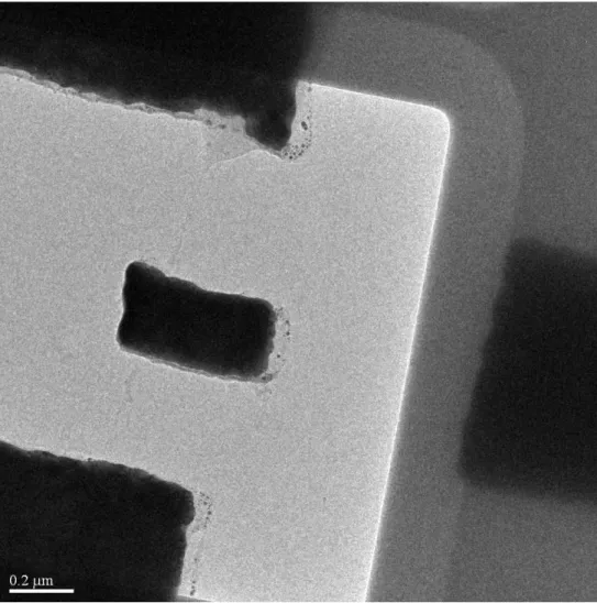
Figure 3.3.7 TEM image of a finished device with one fully suspended CNT and a pedal on it.
3.5 Design and Construction of a Customized Transmission Electron Microscope
Specimen Holder