Modification of Local Structure and Its Influence on Electrical Activity
of Near (310)
5 Grain Boundary in Bulk Silicon
Kentaro Kutsukake
*, Noritaka Usami, Kozo Fujiwara, Yoshitaro Nose,
Takamasa Sugawara, Toetsu Shishido and Kazuo Nakajima
Institute for Materials Research (IMR), Tohoku University, Sendai 980-8577, Japan
We report on the modification of the local structures of (310)5 grain boundary in bulk silicon as the growth of crystal and its influence on electrical activity. The grain boundary was formed via floating-zone growth method utilizing bicrystal seed. The misalignment of the seed resulted in formation of the grain boundary with small deviations of crystal orientation from the5 singular coincidence orientation. The deviations consist of tilt and twist components and they were found to monotonically decrease with respect to the distance from the seed crystal accompanied by the decrease in density of dislocations on the grain boundary. The change in the grain boundary structure allows a systematic study on the correlation between the structure and the electrical activity at the GB. The density of dislocations was found to control the electrical activity and the (310)5 coincidence grain boundary without any dislocations is expected to show a very low electrical activity.
[doi:10.2320/matertrans.48.143]
(Received October 13, 2006; Accepted December 22, 2006; Published January 25, 2007)
Keywords: silicon, bicrystal, grain boundary, dislocation, electrical activity
1. Introduction
Multicrystalline silicon is widely used in solar cell production because of its lower production costs of material as compared to single crystalline silicon. The disadvantage of this material is the presence of extended crystal defects, mainly grain boundaries (GBs) and dislocations, some of which will act as recombination centers of photo generated carriers. The electrical activity on the GB is of fundamental interest and the subject of intensive investigations.
It is commonly known that the electrical activities of GBs are affected by their structure, which can be described by the GB character ( value) and the boundary plane.1) Several researchers have studied the electrical properties of the frequently observed3n GB series and reported that low GBs, especially (111)3 GB, show lower electrical activity than high and random GBs.2–4) These trends are most likely connected with the GB energy due to the fact that the experimentally measured carrier recombination velocity shows similar trend with the theoretically calculated GB energy.5–8)Few researchers have paid much attention on the GB dislocations which are introduced on the GB to compensate the deviation of the crystal orientation from the singular coincidence GB. Seifertet al.have shown that even if the characterized GBs have the same value, the GBs electrical activities varied due to the dislocation density.9)
This paper deals with (310)5 GB, which has been known to have low GB energy, i.e., 0.42 and 0.26 Jm2 provided in model A and B, respectively.10–12) These values are com-parable with that of (221)9 GB, i.e., 0.32 or 0.29 Jm2.13,14) However, no experimental studies have been reported presumably due to its experimental difficulties originating from the different rotation axis between5 GB and3nGB series. We attempted to artificially realize the (310)5 GB in bulk silicon using floating-zone (FZ) growth method utilizing bicrystal seed and studied the GB structure and its electrical
activity by means of spatially resolved x-ray diffraction (XRD), transmission electron microscope (TEM) and mono-chromatic light beam induced current (MBIC). The misalign-ment of the seed caused a small deviation of the crystal orientation from the5 singular coincidence orientation. The deviation was found to monotonically decrease with respect to the distance from the seed crystal accompanied by the decrease in the density of the GB dislocations. The electrical activity was found to relate with the GB dislocation density, and the (310)5 coincidence GB without any GB disloca-tions show a very low electrical activity.
2. Experimental Procedure
The (310) 5 GB was formed in bulk silicon using bicrystal seed via FZ growth method under ultra-high vacuum to avoid impurity diffusion from the crucible surface and atmosphere.15,16)The bicrystal seed was prepared in the following steps as shown in Fig. 1(a). The monocrystalline silicon (001) rod with a diameter of 8.0 mm was cut along the (310) plane into two crystals. One of the crystals was rotated by 180 degree around the [310] axis perpendicular to the cut surface, and the two crystals were bound by a platinum wire. Thus the GB is supposed to consist of (310)5 relation.
The crystal growth was carried out by heating the sample with an electron beam generated from a ring-like tungsten filament (ULVAC YDR500 EB-Z) (Fig. 1(b)). The growth chamber is equipped with a sputter ion pump and a turbo molecular pump and during growth the pressure was in the order of about108Torr. After forming a melt zone between the seed and source crystal, they were pulled down at a constant pulling rate of 1.0 mm/min. The seed and source crystal were B doped (p-type) Si with a resistivity of 50 cm. Sample of the grown crystal is shown in Fig. 1(c).
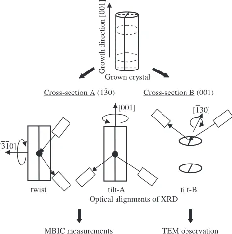
For experimental investigations, the grown crystal was cut along the two different cross-sections as shown in Fig. 2. i.e., theð1330Þsurface that is parallel to the growth direction and perpendicular to the GB plane (cross-section A) and the (001) *Graduate Student, Tohoku University
surface that is perpendicular to the growth direction (cross-section B).
In order to precisely determine the relative crystal orientation of the GB, i.e. the deviations from the (310)5 singular coincidence orientation,!-scan of spatially resolved XRD (Bruker AXS D8DISCOVER) was performed using Cu-K1 and K2 radiation sources with 40 mA and 40 kV. The x-ray spot size was 0.7 mm0.5 mm on the specimen surface and the resolution of crystal orientation was less than 0.01in!scan. The optical alignments of XRD are shown in Fig. 2. On the basis of the GB plane, the deviations can be expressed into three components, two tilts and one twist. The twist and tilt-A which rotate around the [001] axis parallel to the growth direction were determined by analyzing the cross-section A, while tilt-B which rotate around the½1130axis on the GB plane and perpendicular to the growth direction was determined by analyzing the cross-section B.
For the TEM observation, the specimens having the GB were cut from the cross-section B and processed with a mechanical grinding and ion thinning. TEM investigation was performed using JEOL JEM-2000EX (200 kV). On the other hand, MBIC measurement was done utilizing a simple solar cell process that consist of a phosphorus diffusion to form p-n junction, deposition of indium-tin oxide (ITO) as an antireflective coating (ARC) and formation of a front (silver) and back (aluminum) contacts on the cut sample from the cross-section A. The light source of the MBIC measurement is Xe lamp having a spot diameter of 8.0mmon the sample surface with intense emission lines in infrared range.
3. Results
Figure 3 shows the XRD profiles of!-scan around (a) tilt-A and (b) twist axes on different distances from the seed. The x-ray was incident on the GB and its surroundings. Note that in our measurement, we selected the ð2660Þ reflection plane that is perpendicular to the (310) plane. The angle difference
Growth direction
(310)
180°
Pull down Seed Source
[001] [001]
[310] [310]
[130] [130]
Melt Electron
beam
8mm
Seed Grown crystal
(a) (c)
φ (b)
Fig. 1 (a) Configuration of the seed crystal with (310)5 relationship. (b) Schematic illustration of FZ growth method. (c) Photo image of the grown crystal.
tilt-A
twist tilt-B
Grown crystal
TEM observation MBIC measurements
Optical alignments of XRD
Cross-section A (130) Cross-section B (001)
Growth direction [001]
-[310]
[001] [130]
Fig. 2 Brief overview on the experimental procedure and schematic illustrations of the optical alignments of the XRD analysis.
Intensity
,
I
(arb
.units)
Omega,
ω
Omega,ω
0.0°
(a) (b)
seed 6mm 12mm 18mm
0.0°
-0.2° 0.2° -0.2° 0.2°
[image:2.595.113.483.70.235.2] [image:2.595.324.528.289.483.2] [image:2.595.50.287.290.529.2]between the two XRD peaks represents the deviation of relative crystal orientation from the (310) 5 singular coincidence orientation. The misalignments of the seed crystal were found to be 0.14 and 0.12 degrees for the tilt-A and twist components, respectively. The tilt-B deviation could be controlled to be almost zero because the tilt-B axis was the longitudinal axis of the seed rod. It was found that the deviations of GBs monotonically decrease with respect to the distance from the seed crystal. The values of the deviation at 18 mm were 0.05 and 0.00 degrees for the tilt-A and twist components, respectively. This change in the GB structure allows a systematic study on the correlation between the structure and electrical activity.
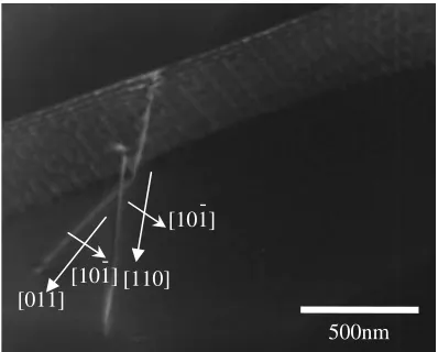
It is believed that GB dislocations are introduced to compensate the deviation based on the displacement shift complete (DSC) lattice. In the case of the (310) 5 GB of diamond structure, six possible GB dislocations are expected, namely: (a) two dislocations with shortest Burgers vector perpendicular to the [001] axis, i.e., bE =a=10½310 per-pendicular to the (310) GB plane and bS=a=10½1330 parallel to the (310) GB plane, (b) four dislocations with short Burgers vector, bD1 =a=10½125, bD2 =a=10½2115, bD3=a=10½1255 and bD4=a=10½21155.17) Figure 4(a) shows the TEM image of the GB at 1 mm from the seed. Hexagonal network of GB dislocations are observed which mainly regarded as screw dislocations with Burgers vector bS and mixed dislocations with Burgers vector bD3 and bD4 to compensate the twist deviation. The disorder of the network might be attributed to interaction with the edge dislocations with Burgers vector bEthat compensate the tilt-A deviation. In fact, in the other part of same specimen, we observed regularly aligned the edge dislocations. On the other hand, Fig. 4(b) shows the GB at 20 mm from the seed. Only the edge dislocations were observed, which is consistent with the absence of the twist deviation.
Since the GB dislocations cannot exist in bulk crystal, the GB dislocations should make crystal lattice dislocations with Burgers vectora=2h110i to escape from the GB plane. The possible combinations of the Burgers vectors of the GB dislocations are,
a=2½1011 ¼a=10½310 þa=10½21155 ð1Þ
a=2½1110 ¼a=10½310 þ2a=10½1330: ð2Þ
In fact, formations of the lattice dislocation with Burgers vector a=2½1011 were observed in the other part of the
specimen at 1 mm from the seed as shown in Fig. 5. If the combination of eq. (2) also ocuured, it should provide faster reduction of the screw GB dislocations than the edge GB dislocations as the growth proceeds. Consequently, the edge GB dislocations will remain. This is in good agreement with our mentioned results (Fig. 4(b)).
On the other hand, MBIC measurement will provide information on electrical activity of the GBs. Figure 6 shows MBIC profiles across the GB at the various distance from the seed measured using an incident wavelength of 993 nm. The depth of the dip caused by the carrier recombination at the GB monotonically decreased with respect to the distance from the seed crystal. This means that the electrical activity of the GB was improved with the growth of the crystal.
4. Discussions
The deviation angles from the 5 singular coincidence orientation,i, are related to the GB dislocation spacing,di, similar to the low angle boundaries, are expressed as
di¼ bi
2 sin
i
2
; ð3Þ
wherebiis the length of Burgers vector of the GB dislocation. The subscripts ‘‘i’’ indicates the component of deviation and
200nm 500nm
(a) (b)
[130]
-[125]
[215]
-[001]
-[310]
Fig. 4 TEM images of the GB at (a) 1 mm from the seed, there is a network of GB dislocations with Burgers vector ofa=10½1330,
a=10½1255, anda=10½21155. (b) 20 mm from the seed, only edge dislocations with Burgers vector ofa=10½310are observed.
500nm [110]
[011]
[101]
[101]
-Fig. 5 TEM images of the GB on the other part of the same specimen shown in Fig. 3(a). Crystal lattice of 60dislocations with Burgers vector
[image:3.595.131.471.74.202.2] [image:3.595.327.526.256.416.2]types of the GB dislocations. The dislocation spacings given in eq. (3) using the deviation angle and the observed dislocation spacings with TEM are summarized in Table 1. The calculated value and the TEM results are in good agreement.
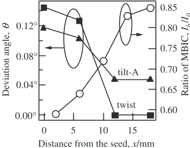
The modification in the local GB structure as the growth of crystal was found to produce the change in electrical activity of the GB. Figure 7 shows the deviation angles for the tilt-A and twist components and ratio of the MBIC at GB, Ib, to MBIC in the grain,I0, as a function of the distance from the seed. Both the deviation angles and the ratio of MBIC showed monotonic change with respect to the growth of the crystal. We found out that a decrease in deviation angles while an increase in MBIC ratio are observed. These results suggest that the GB structure transformed into more stable structure similar to a singular coincidence 5 GB, thus the electrical activity of the GB significantly reduced.
In order to quantitatively estimate the electrical activities of the GB, we calculated recombination velocities of the generated carriers at the GB, by numerically fitting the MBIC profiles using Zook’s equation.18) The correlation between the recombination velocity and the calculated GB dislocation density is shown in Fig. 8. The recombination velocity was found to increase proportional to the GB dislocation density. Therefore, it is likely that the electrical properties of the GB dislocation, namely the defect energy level, Ei, and the electron capture cross-section,i, are constant in the range of
this dislocation spacing. The GB carrier recombination can be shown as sum of the intrinsic carrier recombination of the singular coincidence GB and the additional carrier recombi-nation of the GB dislocations can be expressed based on the Shockley-Read-Hall (SRH) model with low injection level19)
v¼vþ X
i
AiNi¼vþ X
i 2Ai
bi
sinði=2Þ; ð4Þ
while
Ai¼
iVth
1þexp
EiEf kT
;
wherev and v are carrier recombination velocities of the GB and singular coincidenceGB, respectively, andNi,Vth, Ef,kandT are the GB dislocation density, thermal velocity of free electron, Fermi energy level, Boltzmann constant and temperature, respectively. It is assumed that the proportional constant Ai of the edge and the screw dislocations are comparable. This assumption has been supported by a report of crystal lattice dislocations.20) The fitting of the
exper-MBIC intencity
,
I
(arb
.units)
-400 -200 0 200 400
Position, x/µm
2mm 6mm 10mm 14mm 18mm
[image:4.595.94.245.67.289.2]Fig. 6 MBIC profiles across the GB at the various distances from the seed.
Table 1 Summary of the data on spacings of the edge and screw dislocations on the GB at 1 and 20 mm from the seed.
Dislocation type Distance from Dislocation spacing,d/nm the seed,l/mm XRD TEM
a/10[310]edge 1 70 102
20 205 366
a/10½1330screw 1 82 85
20 0 0
Deviation angle,
θ
15 10 5 0
Distance from the seed, x/mm 0.85
0.80
0.75
0.70
0.65
0.60 tilt-A
twist
0.04°
0.00° 0.08° 0.12°
Ratio of MBIC,
Ib
/
I0
Fig. 7 The deviation angles for the tilt-A and twist components and the ratio of the MBIC at GB,Ib, to MBIC in the grain,I0, as a function of the
distance from the seed.
1.5x10⁴
1.0
0.5
0.0
Carrier recombination velocity,
v
/cm
. sec
-1
1.5x10⁷ 1.0
0.5 0.0
Dislocation density, D/m-1
[image:4.595.328.523.73.225.2] [image:4.595.337.525.293.480.2] [image:4.595.47.293.358.436.2]imental results using eq. (4) suggests thatvis close to zero. This value implies that the singular coincidence 5 GB is expected to be electrically inactive and the electrical activity of the GB mainly due to the carrier recombination of the GB dislocations. The proportional constantAiwas also found out to have a value of 0.1 cm2s1, which is much smaller than 1.5 cm2s1of the (001)1 twist boundary.21)This probably comes from the shorter length of the Burgers vector of the GB dislocation as compared to that of the crystal lattice dislocation. This suggest that a smaller electrical activity of (310)5 GB as compared to that of (001)1 GB with same deviation angle. Furthermore, analysis to determine the value of Ei and i is now in progress and the results will be published elsewhere.
5. Conclusions
The (310) 5 GB in bulk silicon was formed via FZ growth method utilizing bicrystal seed. The misalignment of the seed resulted in formation of the GB with small deviations of crystal orientation from the 5 singular coincidence orientation. The deviation was found to monot-onically decrease with growth of the crystal accompanied by the decrease in density of dislocations on the GB. The density of the dislocations was found to control the electrical activity. Furthermore, the (310) 5 coincidence GB without any dislocations is expected to show very low electrical activity.
Acknowledgement
We would like to acknowledge R. Shimokawa, and G. Sazaki for fruitful discussions and S. Ito for technical his help on TEM observation. A. C. Alguno and R. Nihei are also acknowledged for their critical reading of this manuscript. This work was supported in part by New Energy and
Industrial Technology Development Organization (NEDO) of Japan.
REFERENCES
1) V. Randle: Acta Mater.46(1997) 1459–1480.
2) R. Shimokawa and Y. Hayashi: J. Appl. Phys.59(1986) 2571–2576. 3) A. Bary and G. Nouet: J. Appl. Phys.63(1988) 435–438.
4) Z. J. Wang, S. Tsurekawa. K. Ikeda, T. Sekiguchi and T. Watanabe: Int. Sci.7(1999) 197–205.
5) M. Kohyama, R. Yamamoto and M. Doyama: Phys. Status Solidi B138
(1986) 387–397.
6) M. Kohyama and R. Yamamoto: Phys. Rev. B50(1994) 8502–8522. 7) J. Chen, T. Sekiguchi, D. Yang, F. Yin, K. Kido and S. Tsurekawa:
J. Appl. Phys.96(2004) 5490–5495.
8) J. Chen, D. Yang, Z. Xi and T. Sekiguchi: J. Appl. Phys.97(2005) 033701–033706.
9) W. Seifert, G. Morgenstern and M. Kittler: Semicond Sci. Technol.8
(1993) 1687–1691.
10) M. Kohyama, R. Yamamoto, Y. Ebata and M. Kinoshita: J. Phys.21
(1988) 3205–3215.
11) J. Hornstra: Physica26(1960) 198–208.
12) J. J. Bacmann, A. M. Papon, M. Petit and G. Silvestre: Phil. Mag. A51
(1985) 697–713.
13) R. E. Thomson and D. J. Chadi: Phys. Rev. B29(1984) 889–892. 14) D. P. DiVincenzo, O. L. Alerhand, M. Schluter and J. W. Wilkins:
Phys. Rev. Lett.56(1986) 1925–1928.
15) M. Kitamura, N. Usami, T. Sugawara, K. Kutsukake, K. Fujiwara, Y. Nose, T. Shishido and K. Nakajima: J. Crys. Growth280(2005) 419– 424.
16) N. Usami, M. Kitamura, T. Sugawara, K. Kutsukake, K. Ohdaira, Y. Nose, K. Fujiwara, T. Shishido and K. Nakajima: Jpn. J. Appl. Phys.44
(2005) L778–L780.
17) T. Vystavel, V. Paidar, A. Gemperle and J. Gemperlova: Int. Sci.5
(1997) 215–222.
18) J. D. Zook: Appl. Phys. Lett.37(1980) 223–226.
19) W. Shockley and W. T. Read, Jr.: Phys. Rev.87(1952) 835–842. 20) S. Kusanagi, T. Sekiguchi and K. Sumino: Appl. Phys. Lett.61(1992)
792–794.