University of Warwick institutional repository: http://go.warwick.ac.uk/wrap
A Thesis Submitted for the Degree of PhD at the University of Warwick
http://go.warwick.ac.uk/wrap/49672
This thesis is made available online and is protected by original copyright.
Please scroll down to view the document itself.
AUTHOR:Dagmar Kreikemeyer Lorenzo DEGREE: Ph.D.
TITLE:Photoelectron diffraction determination of adsorbate structures
DATE OF DEPOSIT: . . . .
I agree that this thesis shall be available in accordance with the regulations governing the University of Warwick theses.
I agree that the summary of this thesis may be submitted for publication. I agree that the thesis may be photocopied (single copies for study purposes only).
Theses with no restriction on photocopying will also be made available to the British Library for microfilming. The British Library may supply copies to individuals or libraries. subject to a statement from them that the copy is supplied for non-publishing purposes. All copies supplied by the British Library will carry the following statement:
“Attention is drawn to the fact that the copyright of this thesis rests with its author. This copy of the thesis has been supplied on the condition that anyone who consults it is understood to recognise that its copyright rests with its author and that no quotation from the thesis and no information derived from it may be published without the author’s written consent.”
AUTHOR’S SIGNATURE: . . . .
USER’S DECLARATION
1. I undertake not to quote or make use of any information from this thesis without making acknowledgement to the author.
2. I further undertake to allow no-one else to use this thesis while it is in my care.
DATE SIGNATURE ADDRESS
. . . .
. . . . . . . .
. . . .
Photoelectron diffraction determination of
adsorbate structures
by
Dagmar Kreikemeyer Lorenzo
Thesis
Submitted to the University of Warwick
for the degree of
Doctor of Philosophy
Physics
Contents
List of Tables iii
List of Figures iv
Acknowledgments xiv
Declarations xvi
Abstract xviii
Abbreviations xix
Chapter 1 Introduction 1
1.1 Organisation of the thesis . . . 3
Chapter 2 Experimental Details 5 2.1 Synchrotron radiation . . . 6
2.2 X-ray photoelectron spectroscopy . . . 9
2.3 Photoelectron Diffraction . . . 11
2.3.1 Description . . . 12
2.3.2 Theoretical background . . . 14
2.3.3 Experimental setup . . . 18
2.3.4 Data collection . . . 23
2.3.5 Structure determination . . . 25
2.3.6 Error determination . . . 25
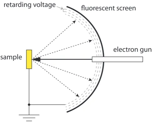
2.4 Low energy electron diffraction . . . 27
2.5 Near edge X-ray absorption fine structure . . . 29
3.2 The adsorption site of the methoxy species on Cu(110) . . . 40
3.2.1 PhD Results . . . 45
3.3 Discussion . . . 53
3.3.1 Conclusions . . . 54
Chapter 4 The formate species on Cu(110) and Cu(111) 55 4.1 Introduction . . . 55
4.2 Formate on Cu(110) . . . 59
4.2.1 PhD Results . . . 62
4.3 Formate on Cu(111) . . . 65
4.3.1 PhD Results . . . 66
4.4 General discussion and conclusions . . . 71
4.4.1 Conclusions . . . 72
Chapter 5 Reaction intermediates of methanol oxidation under steady-state conditions 74 5.1 Introduction . . . 74
5.2 Results . . . 76
5.2.1 PhD results . . . 81
5.3 Conclusions . . . 83
Chapter 6 The local structure of the phenyl imide reaction interme-diate on TiO2 84 6.1 Introduction . . . 84
6.1.1 The rutile TiO2(110) surface . . . 86
6.2 Results . . . 89
6.2.1 NEXAFS results . . . 90
6.2.2 PhD results . . . 94
6.3 Conclusions . . . 98
List of Tables
3.1 Summary of the chemical shifts between carbon-containing species on the Cu(110) surface. . . 41 3.2 Summary of the chemical shifts between oxygen-containing species
on the Cu(110) surface. The chemical shifts are given in eV. . . 44
4.1 Summary of previous determinations of the Cu-O bond length for car-boxylate species on Cu surfaces. PhD* indicates that these studies used a simplified theoretical modeling that may involve some sys-tematic error. NIXSW does not measure the bond length directly and these ** values rely on certain assumptions about the surface relaxation. . . 57
List of Figures
2.1 Diagram of the synchrotron radiation facility in Berlin, BESSY II (taken from [22]). . . 7 2.2 Schematic diagram of the radiation beam traveling in a curved path
emitting photons from an undulator into a narrow cone of natural emission angle∼=γ−1. The energy of the electrons isE=γmc2. . . . 8 2.3 Design of the UE56-2 PGM-2 beamline at BESSY II in Berlin (not
to scale). . . 9 2.4 Schematic diagram of the photoemission process from a 1s core level.
Eb denotes the binding energy, Ek denotes the kinetic energy and φ
the work function. . . 10 2.5 Schematic diagram representing the photoelectron diffraction
tech-nique, in the scanned-energy mode. Blue atoms depict surface atoms (scatterers) and the red atom is the adsorbate (emitter) atom. The component of the wavefield from the emitter interferes with the com-ponents of the same wavefield scattered by the surrounding atoms. The directly emitted wave is represented in red, in black are the singly-scattered waves and in blue the doubly-scattered waves. . . . 12 2.6 Modulus of the elastic scattering factor for electrons by a copper atom
as a function of scattering angle at several different electron energies, as reported in [8]. All curves are normalised to the scattering factor at zero angle. . . 13 2.7 Schematic diagram showing the forward scattering photoelectron
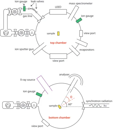
2.8 Front view of the experimental equipment. The chamber consists of two chambers on top of each other separated by a gate valve. The sample can me moved in x, y, and z, and in the polar (θ) and azimuthal angle (φ). . . 19 2.9 Top view of the top and the bottom chamber. The top chamber
is basically used for preparation of the sample and LEED experi-ments, and the bottom chamber is employed for XPS (either with synchrotron radiation or with the external X-ray source), NEXAFS and PhD experiments. . . 21 2.10 Diagram illustrating the operation of an Omicron EA-125HR 125 mm
mean radius hemispherical electrostatic analyser. θdenotes the angle between the beamline and the entrance slit of the analyser. . . 22 2.11 Photoelectron diffraction spectrum of an O 1s core level from HCOO
on a Cu(111) surface. The photoemission intensity of O 1s is mea-sured as a function of kinetic energy at a fixed geometry. The inset shows an individual X-ray photoelectron spectrum. . . 23 2.12 In the upper panel, the photoemission intensity is shown as a function
of photoelectron kinetic energy. The red line represents the intensity,
I(E), and the black dashed line represents the spline,I0(E), to which the intensity is normalised to obtain the modulation function, χ(E) (brown line, lower panel). This data is obtained from the raw data shown in Figure 2.11. . . 24 2.13 Schematic diagram of the estimation of the error of a certain
param-eter, in this case, the height of formate on a Cu(110) surface. The red line represents the line scan around the best-fit value. The blue line depicts the sum of Rmin and the variance, and the black dots
represent the intersection between the parabola of the line scan and the variance. The distance between the vertex of the parabola and the intersection gives the error of the parameter. In this case, the error is symmetric and is∼ 0.03 ˚A (1.86 ˚A ±0.03 ˚A). . . 27 2.14 Representation of the LEED setup. The electron gun provide a
2.15 On the top,a, schematic diagram of the effective potential (left) and the corresponding NEXAFS K-shell spectrum (right) of a diatomic molecule adapted from [12]. On the bottom,b, example of the Auger process, where a photon of energy hν impinges into a core level of an adsorbate atom and creates a hole. This hole can be annihilated via Auger emission. One electron of an outer shell can fill the hole, and in this process the electron loses energy. This energy appears as kinetic energy given to another electron from the outer shell. . . 30 2.16 Example of O 1s NEXAFS spectra of formate on Cu(110), taken from
[40]. The spectra in the left are taken in the [1 1 0] azimuth, and the ones in the right in the [0 0 1] azimuth. The full lines represents the spectra taken at normal incidence, and the dashed lines taken at grazing incidence.The features appearing at lower kinetic energy correspond to theπ features and at higher kinetic energy appear the
σ features. . . 31 2.17 Diagram of near edge X-ray absorption fine structure based on an
example of [12] for a π-bonded diatomic molecule. The molecular axis is normal to the surface. E denotes the polarisation vector of the incident light,Ephot=h·ν, andO denotes the direction of the final
state orbital. In this case, the π-resonance is maximised at normal incidence (left) while at grazing incidence (right) the σ-resonance is maximised. . . 32
3.1 Scheme of the methanol (left) and methoxy (right) molecules. The red balls correspond to the oxygen, the grey to the carbon and the white to the hydrogen atoms. . . 35 3.2 Structure model proposed by Holub-Krappe et al. [44]. The
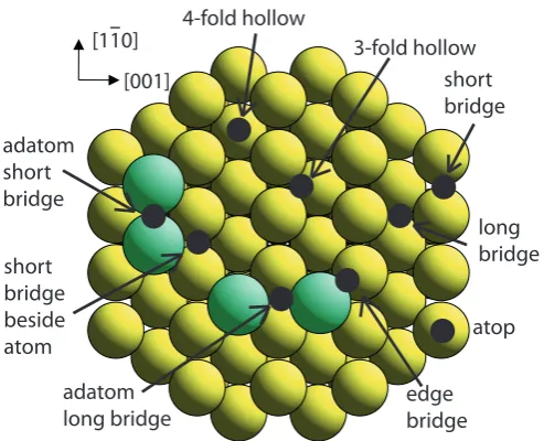
close-packed direction is the [1 1 0] and the perpendicular one is the [001] di-rection. This (4x2) model involves two different low-symmetry three-fold coordinated adsorption sites, A and B. Large circles represent copper atoms and the small circles represent the methoxy molecules. The molecules in A correspond to the species tilted 18◦ in the [1 1 0] direction and the molecule in B is tilted by 40◦ in the [001] direction. 37 3.3 Summary of all the possible adsorption sites on a Cu(110) surface
including Cu adatoms. . . 39 3.4 a) C 1s and b) O 1s XP spectrum of the ”bad” preparation, which
3.5 Comparison of a C 1s XP spectrum taken from a good prepara-tion of methoxy-covered Cu(110) surface, as a result of the exposure to methanol and oxygen, and the spectrum from a formate-covered Cu(110) surface, as a result of a formic acid dosing. The red line depicts the methanol experiment and the blue line depicts the formic acid experiment. The peak corresponding to methoxy and the one corresponding to formate are separated ≈ 1.9 eV, a characteristic chemical shift for these two species. . . 42 3.6 Fit of the a) C 1s and the b) O 1s XP spectra of the ”good”
formate-free preparation. . . 43 3.7 Summary of all the experimental data taken in the two different
az-imuths, [110] and [001]. The spectra taken at 30◦ and 40◦ in the [110] show the largest modulations, up to±20%. . . 45 3.8 Comparison of experimental O 1s PhD spectra with theoretical
simu-lations for five different local adsorption sites on an unreconstructed Cu(110) surface. . . 46 3.9 Representation of a two-site model of a methoxy-covered Cu(110)
with an added row reconstruction. The yellow balls depict the Cu sur-face, the green ones depict the Cu added row atoms, the red ones are the oxygen atoms of the methoxy molecule and the grey balls are the carbon atoms from methoxy. One methoxy molecule is occupying a short bridge site on the added row, and the second methoxy molecule is occupying a short bridge on the underlying unreconstructed surface beside the added row. The hydrogen atoms of the methoxy molecule are not represented here, since PhD is not sensitive to them. . . 48 3.10 Comparison of the experimental (black) and simulated (green) PhD
spectra of the best fit for methoxy on Cu(110) surface. The model simulated here is a two short bridge site, on the Cu added row recon-structed surface, as shown in Figure 3.9. . . 49 3.11 Comparison of the (5x2) model proposed in the literature with PhD
3.12 (5x2) model structure proposed by DFT. The box delimits the unit mesh, which contains 4 Cu adatoms and 4 methoxy species. The green balls are the copper adatoms, the yellow balls correspond to the underlying unreconstructed Cu surface, the red balls are the oxygen atoms, the grey ones are the carbon atoms and the white ones are the hydrogen atoms. . . 51 3.13 Comparison of the experimental data (black) and the theoretical
sim-ulations (red) of a methoxy-covered surface. The model simulated here is the so-called ”zig-zag” structure, a (5x2) reconstruction in-cluding Cu adatoms. This model was optimised by DFT and after-wards reoptimised by PhD to find the best fit. The overall R-factor is 0.14. The individual R-factors are 0.28 for normal emission, 0.11 for 30◦ and 0.09 for 40◦. . . 52 3.14 Comparison of the simulated STM image of the (5x2) methoxy-covered
Cu(110) surface (left) obtained from the DFT calculations based on the (5x2) model corresponding to the ”zig-zag” structure found here, with an experimental image (right, [49]). The rectangle superimposed in the image depicts a (5x2) unit mesh. . . 53
4.1 Scheme of the formic acid (left) and formate (right) molecules, where red corresponds to oxygen, grey to carbon and white to hydrogen . . 56 4.2 Summary of all the proposed adsorption sites for formate on the three
low-index copper surfaces, where ”a” represents a bridge site with the oxygen atoms in four-fold hollow sites, ”b” represent an atop site with the oxygen atoms in bridge sites, ”c” represents an atop diagonal site and ”d” represents a short bridge site. . . 57 4.3 O 1s a) and C 1s b) XP spectra of the dosed sample (red), after PhD
scan (black) and after annealing (grey). This spectra are taken at 140 K. An extra feature shifted 1.2 eV from the main peak towards higher binding energies appears after the PhD scan. This new peak corresponds to a small contamination of water and formic acid. These spectra are taken at 20◦ of polar angle. . . 60 4.4 Fit of the O 1s XP spectrum taken immediately after the PhD scan.
4.5 Comparison of the experimental (black) and simulated (red) PhD spectra of the best fit for formate on Cu(110). The simulation curves are for a short bridge site along the [1 1 0] with the oxygen atoms sitting off-atop the copper atoms. . . 63 4.6 Representation of a formate molecule bonding to the Cu(110) surface
in a short bridge site along the [1 1 0] direction. The orange balls represent the copper atoms, the red ones represent the oxygens and the grey one represents the carbon atom. The hydrogen atom of the molecule is not represented since the PhD technique is not sensitive to it. . . 64 4.7 Comparison of the experimental and theoretical curves for two
differ-ent adsorption sites. The black dotted curves lines are experimdiffer-ental curves. In the left the blue curves are the simulations for an atop site with the oxygen atoms in short bridge sites. On the right, a long bridge adsorption site is simulated (green). Here the molecular plane is parallel to the [001] azimuthal direction. . . 64 4.8 a) O 1s and b) C 1s XP spectra of the dosed sample immediately
before the PhD scan (red), after the PhD scan (black), and after a short annealing to RT (grey), taken at normal emission. The same effect as for formate on Cu(110) was observed: increased intensity at higher binding energy can be seen, but this vanishes after a short annealing to room temperature. . . 66 4.9 Fit of the O 1s XP spectrum taken after the PhD scan. The peak
at 115.8 eV corresponds to formate, whilst the peak at 114.6 eV is assigned to a contamination of water and a multilayer of formic acid, as in the case of formate on Cu(110). . . 67 4.10 Summary of all the modulation functions, χ(E,) taken at different
polar angles at two different azimuthal directions, [1 1 0] and [001]. For angles bigger than 15◦ the modulations are very small. . . 68 4.11 Comparison between the multiple scattering simulations and the χ
4.12 Representation of a formate molecule bonding to the Cu(111) surface in a bridge site along the [1 1 0]. The orange balls represent the copper atoms, the red ones represent the oxygens and the grey one represents the carbon atom. The hydrogen atom of the molecule is not represented since the PhD technique is not sensitive to it. . . 70 4.13 Comparison between theχfunctions (dotted black) and the
theoreti-cal curves (purple) for a formate on an atop position with the oxygen atoms in bridge sites. The R-factor for this geometry is 0.67. . . 70
5.1 Sketch of the experimental chamber at the ISISS beamline at BESSY II taken from [88]. The setup consists of an experimental cell con-nected to the beamline through a SiNx window and a hemispherical
analyser attached to the cell through a system of differential pumping stages. The experimental cell can be filled with gases up to the mbar range. . . 76 5.2 Schematic diagram taken from [88] showing the electron trajectories
inside a differentially pumped aperture system a) without electro-static lenses, b) with electroelectro-static focusing lenses included. In this diagram, the electron are traveling from the left to the right. . . 77 5.3 XP spectra of five different methanol and oxygen on Cu(110) data
sets, recorded at different temperatures. On the left, the C 1s spectra measured at hν = 400 eV are represented, and on the right, the O 1s spectra measured athν = 650 eV. The different temperatures and pressures are also shown. . . 79 5.4 Comparison of PhD scans taken under ultra high vacuum (black line),
at 1x10⁻⁵mbar (blue and red lines) and at 1x10⁻³mbar (yellow line). On the left, the PhD scans associated to the peak assigned to formate are shown. On the right, the PhD scans associated to the methoxy peak. The scan measured in UHV was taken at 140 K. The scans at higher pressures were taken at 310 K, 450 K and 510 K. . . 82
6.2 Representation of the azobenzene (left) and aniline (right) molecules, where the blue atoms correspond to nitrogen, the grey atoms corre-spond to carbon and the white atoms correcorre-spond to hydrogen. . . . 86 6.3 An illustration of a rutile TiO2(110) (1x1) bulk-terminated surface.
The blue atoms represent titanium and the red atoms represent oxy-gen. The light red atoms represent the bridging atoms characteristic of this surface. Following the usual chemical convention for oxides, the oxygen atoms are represented as the larger spheres. The unit mesh is represented by the white box. . . 87 6.4 LEED pattern showing the (1x1) unit cell of a TiO2(110) surface,
taken at a kinetic energy of 100 eV. . . 88 6.5 XP spectra for Ti 2p, O 1s, N 1s and C 1s. The grey lines represent
the spectra taken on the clean surface, prior to the dosing. The red lines represent the sample after dosing azobenzene, and the blue lines correspond to the aniline spectra. . . 88 6.6 XPS for Ti 2p, O 1s, N 1s and C 1s of an azobenzene-dosed sample at
room temperature and at 140 K. The red lines represent the spectra taken at room temperature, shown in Figure 6.5, and the yellow lines represent the spectra taken after a dose at 140 K. The cold spectra show the presence of nitrogen and carbon on the sample, but no titanium or oxygen can be seen anymore. This implies the presence of a multilayer on the sample. The C and N peaks are shifted towards higher binding energy with respect to the room temperature dose, characteristic of a multilayer. . . 89 6.7 N K-edge NEXAFS spectrum of the TiO2 sample dosed with
azoben-zene at 140 K (black), resulting in a multilayer. These spectra were taken at normal incidence in the [1 1 0] azimuth. The sample was then sequentially heated up. Spectra taken at 200 K (yellow), 270 K (blue), and at 510 K (red) are shown here. Aπ-resonance appeared at 398 eV. This feature decreased with increasing temperature. . . . 91 6.8 N K-edge NEXAFS spectra of azobenzene (full lines) and aniline
6.9 C K-edge NEXAFS spectra of azobenzene on TiO2, at room tem-perature, at grazing and normal incidence in the two preferential azimuths. Here it is also obvious that theπfeatures look very similar in every geometry, revealing a tilt of the molecule with respect to the surface normal and with no preferential azimuthal direction. . . 93 6.10 C K-edge NEXAFS spectra of aniline on TiO2 taken at room
tem-perature at normal and grazing incidence. The similarities of these spectra and also if compared with the azobenzene data confirm the adsorption of the same surface species, this being a phenyl imide with the molecular plane tilted with respect to the surface normal. . . 94 6.11 Comparison of the N 1sχfunction for aniline (blue lines) and
azoben-zene (red lines) on TiO2 at three different geometries. The main peaks are reproduced by both adsorbates although the modulations for azobenzene are noisier. . . 95 6.12 Comparison of the experimental χ functions (black) with the
theo-retical simulations (red) of a phenyl imide binding in a bridge site to two Ti atoms. The overall R-factor is 0.48. The adsorption site is shown on the right. The bond length between N and Ti is 2.14 ˚
A and the phenyl ring is oriented along the [0 0 1] azimuth with a tilt of 11◦ from the surface normal. . . 96 6.13 Representation of the dependence of the R-factor on the Ti-N bond
length for the two different reoptimised models: in red, the surface relaxations were optimised for the longer bond length of 2.27 ˚A, and in blue the relaxations were optimised for the bond length between N and Ti of 1.77 ˚A. . . 97 6.14 Comparison of the experimental data and theoretical simulations for a
6.15 Representation of a phenyl imide species binding on an atop site on a 5-fold coordinated Ti atom, where the blue atoms represent the titanium atoms, the red ones the oxygens, the green one represents the nitrogen atom, and the grey atoms represent the carbon atoms of the aromatic ring. The hydrogen atoms are not represented, since PhD is not sensitive to them. . . 99 6.16 Schematic model of the clean TiO2 surface showing atom number
Acknowledgments
First, I would like to thank my supervisor Phil Woodruff, for offering me the
oppur-tunity to work on this project and for always being positive and supportive, even when the experiments weren’t as straightforward as we expected. But especially, I
would like to thank him for running the group in such a kind way. It has been a pleasure to work in such a nice, friendly and helpful environment.
Obviously, I am very grateful to the person with whom I spent most of the time during the first three years of my PhD. Thank you, Werner, for your patience
in helping me in my first weeks at the Fritz with the code and with all the Igor macros. It was a lot of fun to share three years of experiments and many scientific
(and non-scientific) conversations in the office with you. I would not have made it without you. And of course, I also have to thank you for teaching me weird Austrian
expressions.
I also want to thank my colleagues at Warwick: David, Tsenolo and Daryl,
for their help in the numerous beamtimes at BESSY and Matt, with the DFT calculations. David, a special thanks for the enormous help with the code and all
my computing problems. Without your help I would have panicked many more times, and it also compensated for the many times you broke the thermocouple at
BESSY. Tsenolo, thank you for answering all my questions from my very first day and for the funny nights at BESSY.
This work could not have been done without our technicians at BESSY, Willy Mahler and Birgitt Zada. Additionally, I want to thank the members of
Also to Dr. Kuhlenbeck’s group for the very interesting beamtime. I learned a lot
about LEED and mixed oxides in those two weeks. Elena, a big thanks for sharing with me very enjoyable lunchtimes.
I would like to thank the whole Molecular Physics department, in particular, Gerard Meijer, for treating me as a ”normal” MP member, even though officially
I was not; and also to Inga and Andrea for running the department so well, and for always being there to help us with so many problems. Thank you to all the PhD students, Diplomanden, Post-Docs, and everyone else, for all the Wandertage,
Christmas parties, wine tastings, Kaffee und Kuchen, and countless social events. You have been my family over these three and a half years in Berlin. Especially I
want to thank two people who have become more than just colleagues. Thank you to Cyndi (ay Dios m´ıo) and Adela for cheering me up in the bad moments, and
sharing with me the good ones.
I don’t want to forget my friends in Madrid, who shared with me my first
steps in the physics business: Pablo G., Eva, Miguel, Sara, Erika and Christian. For the brunches, the cinema evenings, and the dancing nights, I want to thank my
(physicist) friends in Berlin: Mariana, Teo, Roc´ıo, Isa, Jes´us, Hakim, Ania, Eli, and Cristina y Juan. But especially, I want to thank my best friend, Pilar, for taking
such good care of me. I will miss you a lot.
I cannot forget my family, without which I would not have started this
ad-venture. Thanks to my brother Christian and his family, who are very interested in vectors, to my aunt Bego and of course, to my parents. Pap´a y mam´a, gracias por
vuestro apoyo en todos los pasos de mi vida y sobre todo, gracias por creer en mi m´as que yo misma.
And of course, I want to thank the person who has helped and supported me most over the last years, especially the last months. Frank: thanks for helping me
with the Latex problems, for your patience and your understanding, and for all your love even when I was under a lot of stress. Ich freu mich auf unsere gemeinsame
Declarations
This thesis is submitted to the University of Warwick for the admission of the degree
of Doctor of Philosophy. The work presented in this thesis is my own, except where it is stated otherwise. The work presented here was performed at the Fritz Haber
Institute of the Max Planck Society and at the synchrotron radiation facility Berliner Elektronenspeicherring-Gesellschaft f¨ur Synchrotronstrahlung (BESSY) under the
supervision of Professor D.P. Woodruff in the period of May 2008 to December 2011. No part of this material has been previously submitted to this or any other
institution for admission of any degree.
Part of this work was presented at the German National Conferences in
Dres-den 2009 and 2011 and Regensburg 2010; at the 10th International Conference on Atomically Controlled Surfaces, Interfaces and Nanostructures (ACSIN) (Granada,
Spain, 2009); at the 18th International Vacuum Conference (IVC) (Beijing, China, 2010); at the 18th Interdisciplinary Surface Science Conference (ISSC) (Warwick,
England); and at the 28th European Conference on Surface Science (ECOSS) (Wro-claw, Poland, 2011).
Some articles based on this work have been published:
• D. Kreikemeyer-Lorenzo, M.K. Bradley, W. Unterberger, D.A. Duncan, T.J.
Lerotholi, J. Robinson, and D.P. Woodruff,The structure of methoxy species on Cu(110). A combined photoelectron diffraction and density functional
the-ory determination, Surface Science, vol. 605, 193, (2010)
• M.K. Bradley, D. Kreikemeyer-Lorenzo, W. Unterberger, D.A. Duncan, T.J.
Un-derstanding the local structure of a key catalytic reaction intermediate, Physical
Review Letters, vol. 105, 086101, (2010)
• D. Kreikemeyer-Lorenzo, W. Unterberger, D.A. Duncan, M.K. Bradley, T.J.
Lerotholi, J. Robinson, and D.P. Woodruff, Face-Dependent Bond Lengths in Molecular Chemisorption: The Formate Species on Cu(111) and Cu(110),
Physical Review Letters, vol. 107, 046102, (2011)
Abstract
Scanned-energy mode photoelectron diffraction (PhD) is a well-known method to determine quantitatively the local structure of adsorbates at surfaces. In this thesis, it has been employed to determine the adsorption site of a selection of molecules on surfaces.
The adsorption on Cu(110), of methoxy (CH3O), an intermediate in the catalytic
de-composition of methanol (CH3OH), has been studied. O 1s PhD spectra show the strongest
modulation at 30◦ and 40◦ polar emission angles, both in the [1 1 0] azimuth, which is consistent with a bridge position adsorption site in the [1 1 0] azimuth. The subsequent analysis, as well as parallel DFT studies, confirms two bridge adsorption sites, with different bond lengths to the underneath copper atoms. A tilt of the molecules of 37◦ in the [1 1 0] azimuth is also observed, with the carbon atoms pointing in opposite directions for every adsorption site. This tilt creates a zig-zag model, which fits with an old STM [1] study.
Formate (HCOO), a surface intermediate of the catalytic decomposition of formic acid (HCOOH), has been studied on two different faces of copper, Cu(110) and Cu(111). Although the adsorption sites obtained for both surfaces is similar, namely a short-bridge site slightly off atop, a significant difference of≈0.1 ˚A in the copper-oxygen bond lengths is found, being 1.99 ˚A for Cu(111) and 1.90 ˚A for Cu(110).
In this thesis, it is demonstrated that it is possible, though very challenging, to perform PhD successfully under higher pressures. Methanol oxidation on Cu(110) has been studied under reaction conditions. At temperatures below≈450 K, the adsorption sites of methoxy and formate, the most important surface intermediates of this reaction, have been proved to be similar as in the previous studies performed in ultra high vacuum.
A recent investigation of two different organic molecules, azobenzene (C12H10N2)
and aniline (C6H7N), on rutile TiO2(110) and anatase TiO2(101) surfaces with scanning
tunneling microscopy (STM) [2] indicates that both molecules lead the formation of the same superstructure, believed to be of a common species, phenyl imide (C6H5N). PhD has
been exploited to determine the local adsorption site of adsorbed species formed by both molecules on rutile TiO2(110). N 1s photoelectron diffraction data are almost identical for
both molecules, providing further support for a common surface species with the same, or a closely similar. Additional NEXAFS results support these results, implying that the local adsorption site of azobenzene and aniline is indeed the same. PhD results, which show the largest modulation amplitude at normal emission, suggests that the phenyl imide bonds via the N atoms atop a five-fold coordinated surface Ti atom, with the molecular plane tilted with respect to the surface normal, with a N-Ti bond length of 1.77 ˚A.
[1] F. Leibsle, S. Francis, S.Haq, and M. Bowker,Aspects of formaldehyde synthesis on Cu(110) as studied by STM, Surf. Sci. 318, 46 (1994).
[2] S.-C. Li, and U. Diebold,Reactivity of TiO2 rutile and anatase surfaces toward
Abbreviations
• AFM Atomic force microscopy
• BESSY Berliner Elektronenspeicherring-Gesellschaft f¨ur Synchrotronstrahlung
• CAE Constant analyser energy
• CASTEP Cambridge Serial Total Energy Package
• DFT Density functional theory
• EELS Electron energy loss spectroscopy
• ESCA Electron spectroscopy for chemical analysis
• EXAFS Extended X-ray absorption fine structure
• FCC Face-centered cubic
• GGA Generalized Gradient Approximation
• ISISS Innovative Station of In situ Spectroscopy
• LEED Low energy electron diffraction
• MEIS Medium energy ion scattering
• NEXAFS Near edge X-ray absorption fine structure
• NIXSW Normal incidence X-ray standing wavefield absorption
• PhD Scanned-energy mode photoelectron diffraction
• RAIRS Reflection absorption infra-red spectroscopy
• RPBE Revised Perdew-Burke-Ernzerhof
• SEXAFS Surface extended X-ray absorption fine structure
• SR Synchrotron radiation
• STM Scanning tuneling microscopy
• sXPS Soft X-ray photoelectron spectroscopy
• SXRD Surface X-ray diffraction
• TPD Temperature programmed desorption
• TPRS Temperature programmed reaction spectroscopy
• TSP Titanium sublimation pump
• UHV Ultra high vacuum
• UPS Ultra-violet photoemission spectroscopy
• XANES X-ray absorption near-edge structure
• XPD X-ray photoelectron diffraction
Chapter 1
Introduction
Surface science has experienced an enormous boost in the last few decades. This increasing interest arises from the importance of surface properties for many appli-cations in ”real life”. One of the reasons for this interest of surface science is its application in heterogeneous catalysis due to the great amount of chemical reactions that occur on surfaces. The understanding of how the surfaces behave can enhance these catalytic processes. Surfaces are a kind of ”defect” of solid state materials, and breaking the periodicity of a three dimensional solid can lead to changes, for instance, in the surface and electronic structure.
One of the chemical reactions studied in this thesis is the catalytic decom-position of methanol to produce formaldehyde, one of the most extended processes in industry. Approximately 21 million tons of formaldehyde are produced in one year in the whole world. Many catalytic processes, such as the one just mentioned, are very sensitive to the local structure of the surface and of the active sites. If the local geometry of these active sites on the surfaces can be determined, the catalytic reactions might be performed faster and more easily, thus, reducing the time and the cost of the catalytic process. The determination of the local geometry of the reaction intermediates on the surface in a quantitative way is the motivation for the main part of the work presented in this thesis.
reflec-tion absorpreflec-tion infra-red spectroscopy (RAIRS) [6] or electron energy loss spec-troscopy (EELS) [7], the vibrations of molecules on surfaces can be determined. However, these techniques cannot provide quantitative information on the structure of the surface. Surface extended X-ray fine structure (SEXAFS) [8] can determine adsorbate-substrate bond lengths and near edge X-ray absorption fine structure (NEXAFS) [3, 9–12] provides information on the bond lengths within molecular ad-sorbates and also on the bond angles. Other techniques, such as low energy electron diffraction (LEED) [3, 13, 14], or scanned-energy mode photoelectron diffraction (PhD) [3, 8, 15, 16] provide information on the local geometry of surfaces, and also the structure of reconstructed surfaces after adsorbing molecules on them. Den-sity functional theory (DFT) [17–20] calculations have improved in the past years due to the accessibility to better and faster computers. Many DFT studies have been published on the determination of surface structures based on calculated mini-mum energy structures with considerably success, although some of the conclusions of these studies have been proved to be wrong. The combination of two or more of these surface sensitive techniques helps to understand the surfaces better. In this thesis, PhD has been the main technique to investigate the adsorption site of different molecules adsorbed on surfaces.
Scanned-energy photoelectron diffraction exploits the coherent interference between the directly emitted wavefield from a core level of an atom adsorbed on the sample and the components of the same wavefield backscattered by the neighbouring substrate atoms. By scanning the photon energy, the photoelectron energy changes, and the backscattered waves switch in and out of phase with the directly-emitted wave, modulating the intensity. These variations in the intensity depend directly on the relative positions between the emitter (the adsorbate atom) and the scatterers (the neighbour atoms). Information on the bond lengths between the adsorbate and the substrate atoms are also provided. This technique has the advantages that it is elemental and chemical-state specific. PhD has been proved to be a well-established technique in determining surface structures under ultra high vacuum (UHV).
photoelectron spectroscopy has been applied successfully to characterise surfaces at higher-pressures, and STM has been able to take images of surface reactions. However, so far, no quantitative structural method that does not rely on long-range order has been applied under reaction conditions. In this work, scanned-energy mode photoelectron diffraction has been applied under ”high” pressures for the first time in order to determine the local structure of surface intermediates of a chemi-cal reaction under steady-state conditions, thus closing the gap between UHV and industrial processes.
1.1
Organisation of the thesis
This thesis is a report of work performed at the Fritz Haber Institute and the experimental data collected at the synchrotron radiation facility BESSY II, in Berlin, Germany, in the period of May 2008 to December 2011. The work presented here covers the study of the adsorption site of the most important surface intermediates of methanol oxidation, methoxy and formate, on Cu(110) under ultra high vacuum and under reaction conditions. The adsorption of formate on Cu(111) was also studied. Finally the adsorption of two other molecules, azobenzene and aniline, was studied on the (110) face of rutile titanium dioxide. For these investigations, energy-scanned photoelectron diffraction was the main technique used, but in the case of aniline and azobenzene on TiO2 near edge X-ray absorption fine structure was also employed. The organisation of the thesis is the following:
Chapter 2 is concerned with the experimental details related to this thesis. First, details of the beamline at BESSY are provided. X-ray photoelectron spec-troscopy is then introduced. A larger section about photoelectron diffraction is then introduced. This section contains information on the experimental chamber, the theoretical background of the technique and it describes the data collection and the procedure used for the structure determination. Finally, two other complementary techniques are introduced, LEED and NEXAFS.
of experiments and theory. Finally, a discussion is included.
Chapter 2
Experimental details
The goal of this thesis was the determination of the local structure of different ad-sorbates on metal and oxide surfaces. The main technique used for this purpose was scanned-energy photoelectron diffraction (PhD), a well-established structural technique, which provides direct information on the relative positions of the adsor-bate and surface atoms. PhD is based on X-ray photoelectron spectroscopy (XPS), and takes advantage of its elemental and chemical specificity. One of the main advantages of PhD with respect to other structural methods (e.g., LEED) is that it does not require long range periodicity. However, other experimental methods were also employed as a support when PhD could not give an answer to the raised questions. Near edge X-ray absorption fine structure (NEXAFS) was used in the study of nitroaromatic molecules on titanium dioxide to provide extra information on the orientation and tilt of the adsorbates on the surface, information that could not be obtained from PhD. Low energy electron diffraction (LEED) together with XPS were used to characterise the sample and check its cleanliness.
PhD and NEXAFS require the use of a tunable X-ray source with very intense light. For that, all the experiments presented here were performed in the synchrotron radiation facility in Berlin, Germany (BESSY II). XPS can be carried out with synchrotron radiation (SR) or an external source, but in this thesis all the XP spectra were taken also with synchrotron radiation.
2.1
Synchrotron radiation
The electromagnetic radiation emitted when near relativistic charged particles travel in curved paths is called synchrotron radiation [21]. This radiation can be gener-ated over a broad range of wavelengths, from visible light to the hard X-ray of the electromagnetic spectrum. The importance of synchrotron radiation relies on its high intensity, its broad spectral range and other properties such as collimation, polarisation, coherence, etc... These properties make synchrotron radiation a very useful tool for the study of surface science, and in particular, its tunability makes it essential for photoelectron diffraction.
A storage ring synchrotron radiation source is a circular particle accelera-tor that enables a current of electrons to circulate at relativistic velocities for sev-eral hours. A storage ring consists of a sequence of dipole (bending) magnets and quadrupole (focusing and defocussing) magnets joined by field-free regions, called drift spaces. The circular shape of the accelerator allows the electrons to travel in this closed orbit for several hours. Synchrotron radiation is emitted from all curved parts of the ring. Currently there are around fifty synchrotron radiation facilities all over the world, but all the experiments presented in this thesis were carried out in the Berliner Elektronenspeicherring-Gesellschaft f¨ur Synchrotronstrahlung (BESSY II) in Berlin, Germany. BESSY has a circumference of 240 m, with ≈ 50 beam-lines or experimental stations. The beamline where most of the experiments were performed was the UE56-2 PGM-2; only the study of the oxidation of methanol at high-pressures was performed at the beamline ISISS (Innovative Station of In situ Spectroscopy). BESSY II is one of the so-called third generation storage rings. This type of synchrotron source is characterised by lower electron beam emittance and many straight sections for insertion devices, such as wigglers or undulators.
0 10 20 m
Microtron
Elektron gun
Injektor
Synchrotron perimeter 96 m
Storage ring perimeter 240 m
[image:30.595.191.423.136.341.2]Undulator
Figure 2.1: Diagram of the synchrotron radiation facility in Berlin, BESSY II (taken from [22]).
There are three modes of operation in the storage ring in Berlin, depending on how are the electrons injected into it:
1. Mutibunch mode (the one used in this thesis), where around 350 packets are injected in the beam separated by a few nanoseconds.
2. Single bunch mode, where a single packet is injected in the storage ring and every packet returns every 800 ns. This mode is typically used for time resolved experiments.
3. Low-alpha mode. This mode can be operated in single and multibunch mode. Here, the photon pulses are shortened (2 ps vs 30 ps in the normal mode) enabling time resolved experiments in the multibunch mode. Furthermore, the lengths of the electron packets are decreased providing Terahertz radiation.
θ
electron beam
photon beam
Figure 2.2: Schematic diagram of the radiation beam traveling in a curved path emitting photons from an undulator into a narrow cone of natural emission angle∼=
γ−1. The energy of the electrons isE=γmc2.
The cone of light produced by a bending magnet [21] is a continuous band of radiation in the bending plane, with a fan-shaped beam of photons (broad in the horizontal plane but small in the vertical plane). A wiggler is a succession of magnetic poles with alternating polarity. Each pole bends the electron beam through a relative large angle in comparison withmc2/E. These devices are placed in the straight parts of the ring, but because the alternating deflections counteract each other, the beam is not bent and the electrons continue traveling in their orbit. The flux and brightness of the beam are intensified byN (N is the number of poles of the device). An undulator, which is the device used in the UE56-2 PGM-2 at BESSY, works in principle as a wiggler (alternating poles) with the difference that now the bending angle is of the order of mc2/E. In this way, the angle of emission is comparable with the natural emission angle of the synchrotron radiation, ∼=γ−1
( Figure 2.2) and therefore, the intrinsic brightness of the synchrotron radiation is preserved in the horizontal and vertical planes. Also, coherent interference takes place in an undulator resulting in a spectrum enhanced at certain wavelengths, whereas in a wiggler the radiation adds incoherently resulting in a spectrum that is smooth and continuous.
undulator UE56
wall
toroidal mirror
plane mirror
plane grating
cylindrical
mirror exit slit conical mirror
sample
{
1 period monochromator
Figure 2.3: Design of the UE56-2 PGM-2 beamline at BESSY II in Berlin (not to scale).
for the photoelectron diffraction experiments.
Figure 2.3 shows a schematic diagram of the UE56-2 PGM-2 beamline at BESSY II. The photon beam, after passing through the undulator (and the wall separating the storage ring from the experimental hall) encounters a toroidal mir-ror which focuses the beam horizontally and collimates the beam in the vertical direction. After that, the radiation beam passes through the monochromator which comprises a plane mirror, the plane gratings and a cylindrical mirror. The objective of the monochromator is to diffract the beam by a grating (400 l/mm or 1200 l/mm) to select the pertinent energy for the experiment. The plane mirror can rotate in order to achieve a constant beam position and the cylindrical mirror immediately after the plane grating focuses the diffracted photon beam vertically into the exit slit. Finally, the radiation beam travels through a conical mirror, which re-focuses the beam again. The focus of the beam is 20 - 200µm vertically, depending on the settings of the exit slit, and 900µm horizontally. However, the flux density of the spot is too high for the photoelectron diffraction experiments, leading to damage of the sample, so a transfer tube is placed between the last flange of the beamline and the experimental chamber. This transfer tube is around 1.5 m long, and thus defocussing of the light allows the experiments to be carried out. The experiments presented in this thesis require photon energies in the range of 200 to 900 eV. The desired energy can be selected by controlling the undulator and the monochromator. Using the third harmonic of the undulator and with the 400 l/mm grating, energies in the mentioned range were achieved with a high photon flux.
2.2
X-ray photoelectron spectroscopy
Energy
Vacuum level Fermi level
2s
1s
E
bE
kφ
h
ν
e
-Figure 2.4: Schematic diagram of the photoemission process from a 1s core level. Eb
denotes the binding energy, Ek denotes the kinetic energy andφthe work function.
of this technique is that an incoming photon from an X-ray source impinges in a surface inducing the emission of an electron. The only condition that the photon has to fulfill is that its energy (Ephot=h·ν) is greater than the binding energy of the
electron and the work function of the solid (where the work function is the minimum energy required to remove an electron from the Fermi level to the vacuum level). XPS is a very useful tool in surface science, mainly due to its surface specificity. This property is enhanced by the use of the rather low kinetic energies (100 - 900 eV) used in this work, which decreases the inelastic mean-free-path of the photoelectrons and therefore its mean escape depth. This ensures that only electrons from the outermost layers are being detected. Also the choice of the emission angle can determine the surface specificity (at grazing angles the technique is more surface specific than at normal emission).
insensitive to changes in the valence electrons due to, for example, chemical bonding with other atoms in a solid. This property ensures that the technique is element specific. The process of photoemission from a core level is illustrated in Figure 2.4. The energy of the emitted electron,Ek, which is detected by the analyser, is
given by:
Ek=hν−Eb−φ (2.1)
whereφis the work function of the sample, andEb is the binding energy of
a core level with respect to the highest occupied level of the solid, i.e., the Fermi level in the case of a metal and the top of the valence band for a semiconductor.
Another important characteristic of XPS is the possibility of probing the chemical environment of the surface species. Due to this characteristic this tech-nique is also known as ”electron spectroscopy for chemical analysis” (ESCA). The exact binding energy of a core electron from a surface atom depends on the local environment of the sample. Changes in the chemical environment will influence the electronic structure of the atom. Hence, atoms of the same element with different chemical environments will show slightly different binding energies. These changes in the energy are called chemical shifts and can be from tenths of an eV to as much as a few eV. Depending on the bandwidth of the light and the resolution of the detector, these chemical shifts can be resolved.
XPS can be carried out with synchrotron radiation but also with a normal lab-based X-ray source, which makes it a very convenient technique. All XP spectra presented here were taken using synchrotron radiation.
2.3
Photoelectron Diffraction
Photoelectron diffraction is a well-known technique for probing the local atomic environment of adsorbate atoms. One of the main advantages of this technique in comparison with the well-established LEED technique (see section 2.4) is that it provides structural information without the need of long range periodicity. The purpose of this thesis is to determine the adsorption site of different adsorbates on different surfaces. In this section, it will be explained how photoelectron diffraction can solve the local structure problem.
Analyser
directly emitted wave
scattered waves
emitter
scatterers hν
Figure 2.5: Schematic diagram representing the photoelectron diffraction technique, in the scanned-energy mode. Blue atoms depict surface atoms (scatterers) and the red atom is the adsorbate (emitter) atom. The component of the wavefield from the emitter interferes with the components of the same wavefield scattered by the surrounding atoms. The directly emitted wave is represented in red, in black are the singly-scattered waves and in blue the doubly-scattered waves.
2.3.1 Description
Photoelectron diffraction exploits the coherent interference of components of the photoelectron wavefield directly emitted from a core level of an adsorbate atom or a surface localised atom and components of the same wavefield elastically scattered by the neighbouring atoms (see Figure 2.5). The scattering interferences produce variations in the measured photoemission intensity both as a function of emission direction and photoelectron energy, due to phase differences associated with the different scattering pathways [8].
As mentioned before, there are two different modes of operation to obtain structural information: angle scan and scanned-energy photoelectron diffraction. These two different modes arise from the way the electron scattering cross-section depends on the scattering angle and photoelectron kinetic energy. Figure 2.6 shows the modulus of the atomic scattering factor as a function of the scattering angleθ
Cu scattering factor
0.0 0.5 1.0
0 45 90 135 180
scattering angle, θ (°)
nor
malised sca
tt
er
ing fac
tor
, F(
θ
)/F(0) photoelectron kinetic energy (eV)
100 300 500 1100
Figure 2.6: Modulus of the elastic scattering factor for electrons by a copper atom as a function of scattering angle at several different electron energies, as reported in [8]. All curves are normalised to the scattering factor at zero angle.
be to exploit the forward scattering by choosing a relative high kinetic energy. For this procedure, the emitter atom has to lie ”below” the scatterer atoms with respect to the analyser. For emission along the emitter-scatterer direction there is no pathlength difference between the directly emitted wave and the scattered one [8, 15, 16]. Therefore, they interfere constructively. However, if there was a phase shift between the two waves, the interference could be destructive. For this case, at 0◦ scattering angle and for high energies the phase shifts are very small and can be neglected. Hence, there is a maximum in intensity along the axis between emitter and scatterer, as shown in Figure 2.7. This diffraction, known as ”zero-order”, does not depend on the photoelectron wavelength and energy. When the scattering angle starts to increase, the pathlength difference is no longer zero leading to increasing destructive interference and therefore a minimum in the measured intensity. This mode of operation is known as angle scan photoelectron diffraction, or also X-ray photoelectron diffraction (XPD). The main advantage of this mode of operation is the possibility of measuring with a normal X-ray source, Mg or Al Kα
with photon energies of 1253.6 and 1486.6 eV, such as those commonly used in the laboratory, providing high enough kinetic energy. XPD is also commonly used for the characterisation of epitaxial thin films.
Figure 2.7: Schematic diagram showing the forward scattering photoelectron diffrac-tion phenomenon from an adsorbate atom on a surface, taken from [8]. In the upper part of the figure, the resulting form of the photoelectron intensity as a function of the polar emission angle is depicted. The photoelectron intensity shows a peak along the intramolecular direction.
angles greater than ≈ 90◦ (see Figure 2.6). For this backscattering geometry, the scattering paths and therefore the phase shift between emitter and scatterers depend strongly on the photon energy. Backscattering photoelectron diffraction can be resolved in angle or in energy, but is more common to perform the energy-scan mode. In this mode of operation, called scanned-energy photoelectron diffraction (PhD), the intensity of core level photoemission from an adsorbate atom is measured in a specific direction as a function of photon energy. As mentioned before, the directly-emitted wave and the backscattered waves interfere coherently. The backscattered components (by the substrate atoms) of the photoelectron wavefield follow different scattering paths which switch in and out of phase with the directly emitted wave (coming from the adsorbate atom), thus modulating the intensity. This interference behaviour depends directly on the relative position between emitter and scatterer.
In contrast to XPD, this mode of operation requires the use of a tunable X-ray source, such as synchrotron radiation.
2.3.2 Theoretical background
as incident plane waves.
With these three simple assumptions, the final intensity of the photoelectrons can be explained as the square of the modulus of the sum of the directly-emitted and singly-scattered components of the wavefield [8]:
I(k)∝ |cosθk+ X
j cosθr
rj fj(θj, k)W(θj, k)e
(−Lj/λ(k))e(i(krj(1−cosθj)+δj(θj,k)))|2 (2.2)
The first term, cos θk accounts for the polarisation angular dependence of
the directly-emitted wave. In the same way, cosθr denotes the angular dependence of the polarisation at the scattering atoms located at rj relative to the emitter.
The summation is over the scattering atoms denoted by the suffixj. The next two terms account for the atomic scattering factor, fj, as seen before (see Figure 2.6),
and the Debye-Waller factor, which describes the attenuation of the modulations due to thermal vibrations. Both factors depend on the scattering angle,θj, and on
the energy, through the modulus of wavevector,k. The attenuation of the intensity due to inelastic scattering is described byexp(-Lj/λ(k)), whereLj denotes the extra
pathlength that the scattered components have to travel through the crystal with respect to the directly-emitted wave. The last term of the equation accounts for the phase in the coherent interference. The first part, rj(1 - cos θj), describes the
pathlength difference,and the second part, δj, is the scattering phase shift.
This expression can be simplified for scanned-energy photoelectron diffrac-tion. An expansion of Equation 2.2 will lead to a series of terms describing the interference between the directly-emitted wave and every scattered wave and also a series of terms describing the interference between the scattered waves. These cross-terms may be assumed to average to zero, resulting in a much simpler expression, which describes the PhD modulation function,χ:
χ(k)∝X j
cosθr rj
fj(θj, k)W(θj, k)e(−Lj/λ(k))cos(krj(1−cosθj) +δj(θj, k)) (2.3)
However, although this approach is good enough for the understanding of the photoelectron diffraction phenomenology, it has been demonstrated that is not appropriate for a quantitative analysis of the data and can lead to incorrect inter-pretations and to the wrong final structural model [8, 24]. Two of the previous simplifications have to be revised [8]:
The previous plane wave description is a far-field approximation of the outgoing spherical wave from the emitter, but this is not right for near-neighbour atoms, where emitter and scatterers are only separated by∼2 ˚A.
2. Multiple scattering has to be included instead of the single-scattering approximation. This idea was already used for LEED and analysis of photoelectron diffraction experiments using this approximation provided much better results than the previous simplification.
A series of papers by Fritzsche [25–28] describes the basis of the multiple scattering code used for photoelectron diffraction in this work, based on the final state wavefunction being a sum over all scattering pathways that the electron can take from the emitter atom to the detector outside the sample. Each pathway is calculated using a magnetic quantum number expansion. Due to the large number of angular momenta necessary for the multiple scattering calculations using a wave expansion, exact calculations are rather expensive at energies above 30 eV and also very time-consuming [29]. Therefore, certain approximations have to be considered. In a first-order perturbation theory, the electron intensity can be described as:
I(K) =X
R0
|ψ(K,R0)|2 ≈
X R0 X m0 |X l0
ML0(E)BL0(k,R0)|
2 (2.4)
whereKandkaccount for the wavevector outside and inside the crystal, re-spectively. The relation between the two wavevectors is determined by the refraction at the surface potential step. The summation is over all the emitter positions,R0, E is the kinetic energy of the emitted electrons and ML0 are the transition matrix elements from the initial state to the final states. The angular momenta are given by L0= (l0 ,m0). The final state wavefunctions within the crystal are described by the coefficients BL0. Some approximations need to be performed due to the great
complexity of these coefficients, which include all possible scattering effects of all the atoms. Thus, BL0(k,R0)can be expanded as:
BL0(k,R0) =e
−ik·R0A(0)
L0(k,R0) +
X
R1
e−ik·R1A(1)
L0(k,R1,R0)
+X
R1
X
R2
e−ik·R2A(2)
L0(k,R2,R1,R0) +.... (2.5)
doubly-scattered waves and so on. All terms with Ri+1 = Ri from Equation 2.5 can
be excluded as they account for scattering from the same atom, which is not physi-cally possible. The terms corresponding to the final state wavefunctions are further described in a partial wave expansion as a function of spherical harmonics YL0(k),
where L0is the angular momentum. These expansions are described in the following equations:
A(0)L0(k,R0) =i−l0YL0(k) (2.6)
A(1)L0(k,R1,R0) =
X
L1
i−l1YL
1(k)Tl1(R1)GL1L0(R1−R0) (2.7)
A(2)L0(k,R2,R1,R0) =
X
L1
X
L2
i−l2YL
2(k)Tl2(R2)
×GL2L1(R2−R1)Tl1(R1)GL1L0(R1−R0) (2.8)
The coefficients Tlj(Rj) describe the complex scattering phase shifts, δj, of
the atom located atRj relative to the emitter. These terms include also the thermal
vibrations [29] and are described as:
Tlj(Rj) =i·sin(δl)·e(iδl) (2.9)
The coefficients GLi+1Li describe the propagation of the spherical wave in an
angular momentum representation:
GLi+1Li(R) = 4π
X
L2
il0−l1−l2hl
2(kR)Y
∗
L2(R)
Z
dΩYL∗1YLYL2 (2.10)
whereRis the vector between two scattering paths, and hl(x) are the
spher-ical Hankel functions [30].
With these approximations, the electron intensity described in Equation 2.4 becomes:
I(K) =X
R0
|ψ(K,R0)|2 ≈
X R0 X m0 |X l0
ML0(E)BL0(k,R0)| 2 = X R0 X m0 |X l0
ML0(E) s X
i=0
e−ik·RiA(i)
L0(k,Rs, ...R1,R0)|
where the directly-emitted wave corresponds toi= 0, singly-scattered toi= 1, and the maximum scattering order to i= s. In this equation, the phase of the outgoing wave is described by the term e−ik·ri. The final modulation function is
then calculated by normalising the intensity by the non-diffractive intensity.
Vibrations
Thermal vibrations attenuate the amplitude of photoelectron diffraction modula-tions. This effect is caused by a ”phase smearing” due to small changes in the scattering path lengths. In order to include this effect of vibrations, a Debye-Waller factor is included in the electron wavefunction, as for the case of extended X-ray absorption fine structure (EXAFS) [31]. The temperature-dependent Debye-Waller factor assumes that the individual atomic motions are uncorrelated and isotropic. It can be described as [32]:
Wj =exp[−k2(1−cosθj)hσj2i] (2.12)
where k is the wavenumber, θj is the scattering angle and hσj2i describes
the temperature-dependent mean-square relative displacement. This latter term is defined by [31]:
hσ2ji=h(u0·r0j)2i+h(uj·r0j)2i −2h(u0·r0j)(uj·r0j)i (2.13)
where u0 and uj are the displacements of the emitter atom, and the jth
atoms, respectively, and rj denotes the position of the atoms. The vibrational
effects show its maximum at 180◦ backscattering and zero for forward scattering. The modulation attenuation due to thermal vibrations increases exponentially with the kinetic energy of the electrons [32].
2.3.3 Experimental setup
Azimuthal rotation (φ)
z x
y
Polar rotation (θ)
x,y,z manipulation
hν
hν Turbo pumps
Rotary pump
Titanium sublimation pumps
sample manipulator
top chamber
bottom chamber
valves
synchrotron radiation Valves
[image:42.595.136.518.240.538.2]cooling system
above 100 ◦C (120 - 180 ◦C). The baking takes about 20 hours, and is followed by degassing of all the filaments present (e.g., LEED, TSPs, sample holder, etc). After this, the base pressure in the chamber is about 10−10 mbar. The chamber is made of Mu-metal, a nickel-iron alloy with high magnetic permeability. This material is commonly used to screen the experiment from the ambient magnetic fields.
The manipulator can rotate the sample in the polar (θ) and the azimuth angle (φ), and move the sample in x, y and z directions. The manipulator has a liquid nitrogen reservoir which is connected to the sample holder through a copper braid, thereby cooling the sample via thermal conduction.
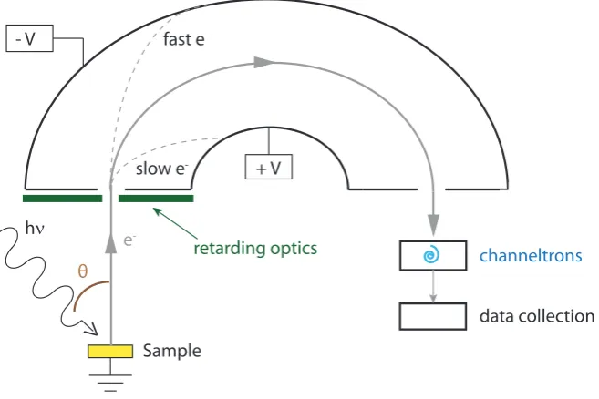
Figure 2.9 shows a top view of the top and the bottom chamber. The top chamber is used for the preparation of the sample. It is supplied with an ion sputter gun, used to clean the sample via ion bombardment, an ion gauge, a mass spec-trometer, a few ports where evaporators can be connected and a LEED optic. The top chamber is also connected to a gas line, separated by a gate valve. In this line different gases and liquids can be attached, e.g., argon, oxygen, methanol or formic acid. All these chemicals are attached to the gas line via leak valves. Also an ion gauge is attached to the gas line to measure the partial pressure. The bot-tom chamber is the actual experimental chamber and therefore it is attached to the beamline. This chamber was attached to the beamline UE56-2 PGM2, at BESSY II. An external X-ray source is also attached to the bottom chamber, which makes it possible to perform some preparatory experiments when there is no access to the synchrotron radiation. An ion gauge, the pumping system and the detector, which is a commercial Omicron EA-125HR 125 mm mean radius hemispherical electrostatic analyser [33], are also attached to the bottom chamber. A schematic diagram of the analyser can be seen in Figure 2.10. The beamline and the analyser are mounted at a fixed angle of 60◦. By rotating the manipulator in θ, the sample can be moved from normal incidence to normal emission (grazing incidence).
hν X-ray source
synchrotron radiation analyser
θ
60°
sample
ion gauge
view port
sample
ion gauge mass spectrometer LEED
view port
view port
evaporators ion sputter gun
gas line
leak valves ion gauge
top chamber
[image:44.595.130.511.161.597.2]bottom chamber
channeltrons
hν
θ
Sample
data collection - V
+ V slow e
-fast e
-retarding optics
e
-Figure 2.10: Diagram illustrating the operation of an Omicron EA-125HR 125 mm mean radius hemispherical electrostatic analyser. θ denotes the angle between the beamline and the entrance slit of the analyser.
will hit the outer (inner) hemisphere and will not contribute to the measured signal. Electrons with the right energy will reach the detector, where seven channel electron multipliers (channeltrons) are placed. Each channeltron is shifted from the position of the central channeltron and they measure spectra which are offset in energy from the true spectra by an amount proportional to the pass energy. In this way, every channeltron is getting extra information and they provide an intensity multiplied by a factor of seven. Then, the channeltrons also amplify the electron flux a factor of 108.
[image:45.595.157.486.115.334.2]300 200
100
120 116 112
In
tensit
y (ar
b. units)
O 1s photoemission spectra
Figure 2.11: Photoelectron diffraction spectrum of an O 1s core level from HCOO on a Cu(111) surface. The photoemission intensity of O 1s is measured as a func-tion of kinetic energy at a fixed geometry. The inset shows an individual X-ray photoelectron spectrum.
2.3.4 Data collection
One energy photoelectron diffraction scan consists of a sequence of (typically around 70) individual X-ray photoelectron spectra from a core level of an atom at a fixed ge-ometry, with fixed energy steps of 4 eV. A typical PhD scan is shown in Figure 2.11. Each scan takes between 1.5 and 2 hours, so to verify that there is no damage, XP spectra are taken right before and after every PhD scan at the same photon energy. This process is repeated for different geometries, varying the polar angle and the azimuth angle. The more geometries are measured, the more accurate is the struc-ture determination. The procedure to obtain the final modulation function (χ(E)) from the raw data begins by normalising the measured intensities of the peaks to the beamline current, I0, which changes with time. The next step is to create a smooth background along the whole range of energy. This is performed by taking an average value of the high kinetic energy tails of two neighbouring peaks. The high energy is chosen over the low energy tail because it is less noisy. The difference between the two values is then subtracted from the second in order to normalise it to the first one. This process is repeated along the whole range of energy of the PhD spectrum.
Intensity (arb. units)
I0(E)
-0.2 0.0 0.2
250 200
150 100
Chi,
I (E)
[image:47.595.127.512.108.338.2]χ
Figure 2.12: In the upper panel, the photoemission intensity is shown as a function of photoelectron kinetic energy. The red line represents the intensity,I(E), and the black dashed line represents the spline, I0(E), to which the intensity is normalised to obtain the modulation function, χ(E) (brown line, lower panel). This data is obtained from the raw data shown in Figure 2.11.
the intensities as a function of photoelectron kinetic energy, I(E), as shown in the upper part of Figure 2.12. In order to extract the non-diffractive effects (e.g., varia-tions of the photoionisation cross-secvaria-tions with the energy, variavaria-tions of the analyser transmission and variations of the monochromator) fromI(E), a spline function is created, I0(E). This spline is depicted also in the upper part of Figure 2.12. The final modulation function,χ, shown in the lower part of Figure 2.12, is then calcu-lated by subtracting this spline function fromI(E) and normalising it with it. It is given by:
χ(E) = I(E)−I0(E)
I0(E)
(2.14)
structural information can be obtained.
2.3.5 Structure determination
The next step is to compare the experimental modulation function with multiple scattering simulations, in a way very similar to that used for quantitative low en-ergy electron diffraction. The method is based on trial-and-error, i.e., the idea is to simulate different possible structures and compare them with the experimental data, adjusting the structure until the agreement is good. In order to quantify this comparison, we use a reliability-factor or R-factor based on that used for LEED [34]. The R-factor for scanned-energy mode photoelectron diffraction is based on the calculation of the location and size of the modulations in intensity due to the diffraction, and these are the values that are compared [35]. The R-factor is calcu-lated from the experimental modulation function,χex, and the modulation function
obtained from multiple scattering theory,χth, as follows [8]:
R=
P
(χth−χex)2 P(χ2
th+χ2ex)
(2.15)
For R = 0 the agreement between theory and experiment is perfect, whereas R = 1 corresponds to uncorrelated data. An R-factor lower than 0.3 is typically considered to be a good result for the PhD technique, although a larger value may be acceptable in some cases. Many parameters can be varied to improve the agreement between experimental data and simulations, namely the location of the adsorbate, relaxations of the surface, interatomic and intramolecular distances, vibrational am-plitudes, inner potentials and scattering parameters. A visual inspection of the sim-ulated data is very important and can also give extra information. For example, if the periodicity and the phase of experimental and simulated data are right, but the relative intensities not, the atom maybe located in the right position but the vibrational amplitudes or the inner potential will be probably wrong. This could lead to a poor R-factor.
2.3.6 Error determination
![Figure 2.1: Diagram of the synchrotron radiation facility in Berlin, BESSY II (takenfrom [22]).](https://thumb-us.123doks.com/thumbv2/123dok_us/9681301.469727/30.595.191.423.136.341/figure-diagram-synchrotron-radiation-facility-berlin-bessy-takenfrom.webp)
![Figure 2.7: Schematic diagram showing the forward scattering photoelectron diffrac-tion phenomenon from an adsorbate atom on a surface, taken from [8]](https://thumb-us.123doks.com/thumbv2/123dok_us/9681301.469727/37.595.261.387.110.277/figure-schematic-diagram-scattering-photoelectron-dirac-phenomenon-adsorbate.webp)


![Figure 3.7: Summary of all the experimental data taken in the two different az-imuths, [110] and [001]](https://thumb-us.123doks.com/thumbv2/123dok_us/9681301.469727/68.595.155.490.106.313/figure-summary-experimental-data-taken-dierent-az-imuths.webp)
