ABSTRACT— This study investigates the optoelectronic properties of nanostructured TiO2/NiO heterojunction solar cells. The heterojunction was fabricated using spray pyrolysis technique at above 350 ºC on Indium Tin Oxide substrate. The X-ray diffraction shows that the heterojunctions have a polycrystalline cubic structure with a preferred orientation along the (1 1 1) and (2 0 0) planes. The elemental properties show the presence of TiO2 and NiO. The optical band gap, refractive index and other optoelectronic properties were also investigated. These findings will enhance the study of cheap, efficient and sustainable alternate materials for solar energy development and affordable energy in developing countries.
Index Terms— Solar energy; TiO2/NiO; Spray Pyrolysis Technique; optical properties; solar cells.
I. INTRODUCTION
lectricity access has direct links to clean drinking water, good health and agricultural activities for rural dwellers [1]. Globally, about 20 % of the population lack access to electricity [2]. Several developing countries still struggle to deliver affordable and stable electricity [3], [4]. Africa is home to about 85 % of the 1.3 billion people in developing countries without access to electricity [5]. The estimated electrification rate of Africa is 32 % [6]. Renewable energy is a viable solution to ending the global electricity and environment problems caused by fossil fuels [7]. There is a vast amount of sunlight incidence in several developing countries to support solar technology [8]. Solar energy can be converted to use direct current electricity using solar cells [9].
A major breakthrough in solar cell fabrication would be large-scale production at an affordable cost [10]. The major obstacle in using silicon solar cells is the expensive nature of the material and the complexities involved in fabricating the solar cells [11]. Apart from the expensive and commercially available silicon-based solar cells, there is
Manuscript received June 01, 2018; revised July 19, 2018. This work was supported by the National Research Foundation and The World Academy of Science (NRF-TWAS) of South Africa under grant number 105492.
O. K. Ukoba is with the University of KwaZulu-Natal, 238 Mazisi Kunene Rd, Glenwood, Durban, 4041, South Africa (corresponding author: Phone: +27640827616 and +2348035431913; e-mail:
[email protected] and [email protected]).
F. L. Inambao is with the University of KwaZulu-Natal, 238 Mazisi Kunene Rd, Glenwood, Durban, 4041, South Africa (e-mail: [email protected]).
difficulty in scaling up existing methods of solar cell fabrication. Most of the available methods for deposition of solar cells requires a stable and steady supply of electricity. This has discouraged manufacturers in developing countries due to their erratic power supply [12].
The solution to such electricity woes may be found in nanostructured metal oxides [13], due to the low cost of processing and the simplicity of deposition methods of nanostructured metal oxides. Nickel oxide (NiO) holds great promise being a p-type metal oxide with a vast range of applications [14], [15], [16].
Several methods have been used to deposit NiO with a view to optimizing it for various applications. The deposition methods include sputtering, hydrothermal growth, sol-gel, and laser ablation [17], [18], [19], [20]. However, the spray pyrolysis technique (SPT) is preferred for films because it allows coatings on large areas in thin layers with uniform thickness [21]. SPT’s simplicity, affordability and the possibilities for mass production singled it out for this study [22]. It requires electricity only during deposition, which can be less than 4 hours per deposition.
This study investigated the optoelectronic properties of a nanostructured metal oxide for possible use in fabrication of affordable and efficient heterojunction solar cells. The optical properties of a metal oxide play a vital role in its usage in the fabrication of optoelectronic devices [23]. The optical properties reveal information relating to the microscopic behaviour of the material.
II. METHODOLOGY
A. Deposition
The chemicals used are of analytical reagent grade and were used without further purification. Distilled and deionized pure water was used during the course of the experiment.
The solar cell was fabricated using a modified SPT as reported by Ukoba, Inambao and Eloka-Eboka [24].
Figure 1 is a pictorial representation of the experimental set-up. Prior to sample preparation, the glass and the indium tin oxide (ITO) coated glass used as substrates were cleaned ultrasonically as reported by Adeoye Abiodun and Salau [25].
Study of Optoelectronic Properties of
Nanostructured TiO
2
/NiO Heterojunction Solar
Cells
Kingsley O. Ukoba, Member, IAENG, and Freddie L. Inambao
The titanium oxide (TiO2) nanostructure thin film was
prepared by mixing 3 ml of titanium ethoxide with 30 ml of distilled water and ethanol mixture, and three droplets of acetic acid. This was stirred for one hour before spraying on cleaned indium tin oxide (ITO) coated glass substrates maintained at about 350 ºC. Deposition parameters such as substrate temperature, carrier gas flow rate and pressure were optimized to obtain quality films.
The nanostructured Nickel oxide (NiO) was deposited on the prepared ITO/TiO2 layers using SPT. The precursor for
NiO was obtained by preparing 0.05 M nickel acetate tetrahydrate in double distilled water.
The precursors were thoroughly stirred for several minutes prior to spraying onto preheated substrates maintained at about 350 ºC. Other deposition parameters were maintained to obtain good quality thin films. The optimized parameters used in the deposition of the NiO
films are tabulated in table 1.
B. Testing
The TiO2 and NiO prepared on ITO were used to study the
elemental, morphological, structural and other optoelectronic characteristics of TiO2 and NiO using Energy
Dispersive X-ray Spectrometer (EDS or EDX: “AZTEC OXFORD DETECTOR”), a ZEISS ULTRA PLUS Field Emission Gun Scanning Electron Microscope (FEGSEM). BRUKER AXS with D8 Advance diffractometer Cu-K α radiation X-ray Diffractometer (XRD) respectively. The weight difference method was also used. Optical properties were studied in the wavelength range of 300 nm to 1000 nm with a SHIMADZU UV-3600UV-VIS Spectrometer. The results of the characterized nanostructured TiO2/NiO
heterojunction solar cells are here reported. III. RESULTS AND DISCUSSION
A. Morphological studies
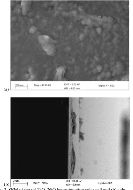
Figures 2a and 2b show the scanning electron micrograph of the heterojunction of p-NiO/n-TiO2 and the side view
respectively. The micrograph reveals scattered distribution and broader flakes of the TiO2/NiO particles across the
surface of the film. The film has even distribution, is adherent to the film surface, and has no cracks. This represents a better surface morphology compared to that of NiO films reported by Sriram and Thayumanavan [26]. This micrograph was obtained by the SEM at the point of interaction between the TiO2 and NiO. It shows a
polycrystalline structure. The micrograph shows the P-type NiO and N-type TiO2 of the thin film with their
polycrystalline structures. It shows complete penetration at the heterojunction.
B. Elemental composition
Figure 3 shows the elemental composition of the TiO2/NiO
heterojunction solar cell deposited on the ITO coated glass substrate. The figure shows the presence of Ti,O, and Ni in the TiO2 and NiO respectively and Indium (In) representing
the ITO coated glass substrate. This confirms the presence of the metal oxides in the heterojunction.
C. Structural analysis
Figure 4 shows the X-ray diffraction patterns of the fabricated TiO2/NiO heterojunction solar cell on the ITO
substrate. The peaks corresponding to NiO and TiO2 were
(a)
[image:2.595.71.207.56.170.2](b)
Fig. 2. SEM of the (a) TiO2/NiO heterojunction solar cell and (b) side
view of the TiO2/NiO heterojunction solar cell
[image:2.595.55.283.437.762.2]Fig. 1. Pictorial representation of the experiment set-up for depositing the TiO2/NiO heterojunction solar cells
[image:2.595.315.545.567.734.2]determined with JCPDS patterns.
The XRD spectrum indicates strong NiO peaks with (1 1 1), (2 0 0) and (2 2 0) preferential orientations. The patterns of the NiO thin film has peak diffractions at (2θ = 37º, 2θ = 43º and 2θ = 64º) for the (1 1 1), (2 0 0) and (2 2 0) planes. The XRD analysis confirms bunsenite which corresponds to the JCPDS card 04-0835 for nickel oxide [27] confirming it as a good absorber layer of solar cells [28]. The TiO2
spectrum also shows strong spectrum and polycrystalline structures typical of N-type in heterojunction solar cells. The structure of the heterojunction indicates that the film is
polycrystalline and chemically pure.
D. Optical properties
The optical properties of a semiconducting material are vital for understanding the electrical properties [29]. Transmittance and reflectance are required for measuring the absorption coefficient. The absorption coefficient measurement gives information about the energy band gap. The energy band gap is a major determinant of the electrical properties of the semiconductor.
Film thickness
The measured data of the film thickness of the heterojunction is depicted in Fig. 5.
The measured film thickness was found to be 4.39 µm. This is due to the joint deposition of TiO2 and NiO on the
ITO.
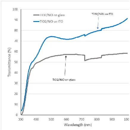
Transmittance
Figure 6 represents the measurement of transmittance for deposited nanostructured TiO2/NiO heterojunction solar
cells.
The graph shows the nanostructured TiO2/NiO deposited
on ITO substrate and a control graph of TiO2/NiO deposited
on glass. The nanostructured TiO2/NiO has a better
transmittance of 91% when compared to that on a glass substrate of 58%. The nanostructured TiO2/NiO deposited
on a glass substrate is denser than the one on ITO substrate. The absorption peak is shifted to lower energies.
Absorbance
Figure 7 shows the absorbance of the TiO2/NiO
heterojunction on ITO and a glass substrate.
Fig. 6. The plot of transmittance of nanostructured TiO2/NiO
heterojunction solar cell
Fig. 5. The film thickness of the nanostructured TiO2/NiO heterojunction
solar cell
Fig. 7. The plot of absorbance of nanostructured TiO2/NiO
heterojunction solar cell
0 0,2 0,4 0,6 0,8 1 1,2 1,4 1,6 1,8 2
300 400 500 600 700 800 900 1000
A
b
so
rb
a
n
ce
Wavelength (nm)
TIO2/NiO on ITO TiO2/NiO on glass
[image:3.595.307.526.153.372.2]TiO2/NiO on glass TiO2/NiO on ITO
[image:3.595.59.288.200.350.2] [image:3.595.55.280.537.693.2] [image:3.595.310.525.577.759.2]This shows marked resemblance to the standard absorbance characteristic of transition metals (to which Ti and Ni belong) [30]. The heterojunction on ITO substrates absorbs more compared to the heterojunction deposited on the glass substrate. This shows that the ITO will perform better. A strong absorbance is an indication of better performance and usage in solar cell fabrication [31].
Absorption coefficient (α)
Absorption coefficient, α was obtained using (1) [32]
(1) Where t is film thickness and A is absorbance.
The absorption coefficient is a vital parameter in the determination of the optical band gap. The absorption coefficient of the nanostructured TiO2/NiO heterojunction
solar cell is shown in Fig. 8.
Optical band gap
The relationship between optical absorption and optical energy band gap is expressed in (2) [33], [34]
α2= C h - E
g (2)
Where C has a constant value, h denotes Planck’s constant, represent incidence light frequency, and Eg
denotes optical energy band gap.
Figure 9 shows a graph of (αh )2 against h for TiO2/NiO
heterojunction deposited on ITO and glass substrate. Extrapolation of Fig. 10 to the h axis for (αh )2 = 0 gives the optical band gap. A shift towards lower energy is observed for optical band gap value. The reduction is attributed to the Moss-Burstein shift [35]. Optical energy band gaps are 3.67 eV and 3.875 eV for ITO and glass substrate respectively.
The ITO substrates value compares favourably with optical band gap reported value of 3.5 eV [36].
[image:4.595.39.239.72.161.2]The quantum size effect may be responsible for the large value of the band gap [37]. Careful and well-optimized deposition parameters also help in obtaining a better optical band gap.
Figure 10 shows the band gap of the TiO2/NiO on ITO with
the trend line and the equation generated. A positive
TABLEI
THE OPTIMUM DEPOSITION PARAMETERS OF SPT Deposition parameter Value
The substrate to nozzle height
20 cm Rate of spray 1 ml/min Spray time 1 min Sprays interval 30 sec
Carrier gas 1 bar filled compressed air
Fig. 9. Graph of (αh )2 against h for nanostructured TiO2/NiO
heterojunction solar cell
Fig. 8. The plot of the absorption coefficient of nanostructured TiO2/NiO heterojunction solar cell
0 1 2 3 4 5 6 7 8
0 200 400 600 800 1000 1200
A
b
s
o
rp
ti
o
n
C
o
e
ff
ic
ie
n
t
Wavelength (nm)
TiO2/NiO on ITO Abs Coeff TiO2/NiO on glass Abs Coeff
TiO2/NiO on glass
TiO2/NiO on ITO
Fig. 10. The gradient of the nanostructured TiO2/NiO heterojunction
[image:4.595.318.540.395.600.2] [image:4.595.52.278.403.602.2]gradient of 0.9419 was obtained as seen from the generated equation shown in (3) and (4).
(3)
(4) IV. CONCLUSION
This study investigated the optoelectronic properties of nanostructured TiO2/NiO heterojunction solar cells
deposited on ITO substrates at 350 °C. The surface morphology shows the P-type NiO and N-type TiO2 of the
thin film with their polycrystalline structures. Both the TiO2
and NiO had complete penetration at the heterojunction. The XRD spectrum indicates strong NiO peaks with (1 1 1), (2 0 0) and (2 2 0) at preferential orientation at 2θ = 37º, 2θ = 43º and 2θ = 64º respectively. Film thickness was found to be 4.39 µm. The nanostructured TiO2/NiO have a better
transmittance of 91 %. Optical energy band gap was 3.67 eV. A positive gradient of 0.9419 was obtained for the TiO2/NiO heterojunction deposited on ITO substrate. This
improved heterojunction is recommended for affordable and efficient solar cells fabrication especially in developing countries.
ACKNOWLEDGMENT
This work was supported by the National Research Foundation and The World Academy of Science (NRF-TWAS) of South Africa under grant number 105492.
REFERENCES
[1] L. T. M. Huynh, and L.C. Stringer, “Multi-scale assessment of social vulnerability to climate change: An empirical study in coastal Vietnam” Climate Risk Management, 20, pp.165-180, 2018. [2] D. Gandini, and A. T. De Almeida, “Direct current microgrids based
on solar power systems and storage optimization, as a tool for cost-effective rural electrification” Renewable Energy, 111, pp. 275-283, 2017.
[3] A. López-González, B. Domenech, D. Gómez-Hernández, and L. Ferrer-Martí, “Renewable microgrid projects for autonomous small-scale electrification in Andean countries” Renewable and Sustainable Energy Reviews, 79, pp. 1255-1265, 2017
[4] N. S. Ouedraogo, “Modeling sustainable long-term electricity supply-demand in Africa” Applied Energy, 190, 1047-1067, 2017.
[5] D. D. Guta, J. Jara, N. P. Adhikari, Q. Chen, V. Gaur, and A. Mirzabaev, “ Assessment of the successes and failures of decentralized energy solutions and implications for the water–energy– food security nexus: Case studies from developing countries”
Resources, 6(3), 24, 2017.
[6] N. Scarlat, V. Motola, J. Dallemand, F. Monforti-Ferrario, and L. Mofor, “Evaluation of energy potential of municipal solid waste from African urban areas” Renewable and Sustainable Energy Reviews, 50, 1269-1286, 2015.
[7] M. M. Savino, R. Manzini, V. Della Selva, and R. Accorsi, “A new model for environmental and economic evaluation of renewable energy systems: The case of wind turbines” Applied Energy, 189, 739-752, 2017.
[8] L. Milagres, N. Rocha, F. Albuquerque, A. Castro, M. Filgueiras, M. Pessoa, J. Novaes, “ Sedentary behavior is associated with lower serum concentrations of vitamin D in Brazilian children” Public health, 152, 75-78, 2017.
[9] A. Islam, and M. Islam, “Status of renewable energy technologies in Bangladesh” ISESCO Science and Technology Vision, 1, 51-60, 2005. [10] M. Eslamian, “Spray-on thin film PV solar cells: advances, potentials
and challenges” Coatings, 4(1), 60-84, 2014
[11] O.K. Ukoba, A. C. Eloka-Eboka, and F. L. Inambao, “Review of nanostructured NiO thin film deposition using the spray pyrolysis technique” Renewable and Sustainable Energy Reviews, 82, 2900 – 2915, 2018. DOI: 10.1016/j.rser.2017.10.041
[12] IRENA. “Solar PV in Africa: Costs and Markets” 2016. Retrieved from http://sun-connect-news.org/fileadmin/DATEIEN/Dateien/New/IRENA_Solar_PV_Cost s_Africa_2016.pdf
[13] E. Serrano, G. Rus, and J. Garcia-Martinez, “Nanotechnology for sustainable energy” Renewable and Sustainable Energy Reviews, 13(9), 2373-2384, 2009.
[14] W. J. Nam, Z. Gray, J. Stayancho, V. Plotnikov, D. Kwon, S. Waggoner, and A. Compaan, “ALD NiO thin films as a hole transport-electron blocking layer material for photo-detector and solar cell devices” ECS Transactions, 66(1), 275-279, 2015.
[15] C.-C. Wu, and C.-F. Yang, “Effect of annealing temperature on the characteristics of the modified spray deposited Li-doped NiO films and their applications in transparent heterojunction diode” Solar Energy Materials and Solar Cells, 132, 492-498, 2015.
[16] Z. Zhu, Y. Bai, T. Zhang, Z. Liu, X. Long, Z. Wei, and F. Yan, “High‐performance hole‐extraction layer of sol–gel‐processed NiO nanocrystals for inverted planar perovskite solar cells” Angewandte Chemie, 126(46), 12779-12783, 2014
[17] M. M. A. Hussein, “Optical and structural characteristics of NiO thin films doped with AgNPs by sputtering method” INAE Letters, 2(1), 35-39, 2017
[18] S. Kerli, and U. Alver, “Preparation and characterisation of ZnO/NiO nanocomposite particles for solar cell applications” Journal of Nanotechnology, 2016.
[19] B. Sasi, and K. Gopchandran, “Preparation and characterization of nanostructured NiO thin films by reactive-pulsed laser ablation technique” Solar Energy Materials and Solar Cells, 91(15-16), 1505-1509, 2007
[20] K. Zrikem, M. Da Rocha, A. A. Aghzzaf, M. B. Amjoud, D. Mezzane, and A. Rougier, “Optimization of NiO thin films by sol-gel for electrochromic properties” ECS Meeting Abstracts. Abstract MA2017-01 1866, 2017
[21] V. Gowthami, P. Perumal, R. Sivakumar, and C. Sanjeeviraja, “Structural and optical studies on nickel oxide thin film prepared by nebulizer spray technique” Physica B: Condensed Matter, 452, 1-6, 2014
[22] M. G. Faraj, “Effect of aqueous solution molarity on the structural and electrical properties of spray pyrolysed lead sulfide (PbS) Thin Films” International Letters of Chemistry, Physics and Astronomy, 57, 122, 2015
[23] V. Gowthami, M. Meenakshi, P. Perumal, R. Sivakumar, and C. Sanjeeviraja, “Optical dispersion characterization of NiO thin films prepared by nebulized spray technique” Int. J. ChemTech. Res, 6(13), 5196-5202, 2014
[24] O. K. Ukoba, F. L. Inambao, and A. C. Eloka-Eboka, “Fabrication of affordable and sustainable solar cells using NiO/TiO2 PN heterojunction” International Journal of Photoenergy, 2018, 7. doi:https://doi.org/10.1155/2018/6062390
[25] A. E. Adeoye, and A. Salau, “Effect of annealing on the structural and photovoltaic properties of cadmium sulphide: copper sulphide (Cds: Cuxs) heterojunction” International Journal of Scientific and Research Publications, 5(8), 2015
[26] S. Sriram, and A. Thayumanavan, “Structural, optical and electrical properties of NiO thin films prepared by low cost spray pyrolysis technique” International Journal of Materials Science and Engineering, 1, 118-121, 2013
[27] M. Gabal, “Non-isothermal decomposition of NiC2O4–FeC2O4 mixture aiming at the production of NiFe2O4” Journal of Physics and Chemistry of Solids, 64(8), 1375-1385, 2003.
[28] N. A. Bakr, S. A. Salman, and A. M. Shano, “Effect of co doping on structural and optical properties of NiO thin films prepared by chemical spray pyrolysis method” International Letters of Chemistry, Physics and Astronomy, 41, 15—30, 2015
[29] G. Benno, and K. Joachim, “Optical properties of thin semiconductor films” 2003. Retrieved from: home.fnal.gov/~jkopp/tum/pdf/F/hl_spekt.pdf
[30] A. Axelevitch, B. Gorenstein, and G. Golan, “Investigation of optical transmission in thin metal films” Physics Procedia, 32, 1-13, 2012 [31] S. Ezugwu, F. Ezema, R. Osuji, P. Asogwa, A. Ekwealor, and B.
Ezekoye, “Effect of deposition time on the band-gap and optical properties of chemical bath deposited CdNiS thin films”
Optoelectronics and Advanced Materials–Rapid Communications, 3(2), 141-144, 2009
[32] J. Barman, K. Sarma, M. Sarma, and K. Sarma, “Structural and optical studies of chemically prepared CdS nanocrystalline thin films”
properties of chemical bath deposited PbS-CuS thin films” Journal of Optoelectronics and Advanced Materials, 11(7), 940-944, 2009. [34] V. Estrella, M. Nair, and P. Nair, “Semiconducting Cu3BiS3 thin
films formed by the solid-state reaction of CuS and bismuth thin films” Semiconductor Science and Technology, 18(2), 190, 2003. [35] T. Moss, “The interpretation of the properties of indium antimonide”
Proceedings of Physical Society, Section B, 67(10), 775, 1954. [36] G. Boschloo, and A. Hagfeldt, “Spectroelectrochemistry of
nanostructured NiO” The Journal of Physical Chemistry B, 105(15), 3039-3044, 2001.