International Journal of Computer Applications (0975 – 8887) Volume 179 – No.52, June 2018
Beam Steering Controller Architectures for an Active
Electrically Scanned Array Antenna: Comparison and a
Cost Effective Implementation
Angelo Manco
Electronics and Communications
CIRA Italian Aerospace Research Centre
81043 - Capua - Italy
Vittorio Ugo Castrillo
Electronics and Communications
CIRA Italian Aerospace Research Centre
81043 - Capua - Italy
ABSTRACT
Within the TELEMACO project, the development of an inno-vative avionic radar system for advanced land monitoring, provided with an Active Electrically Scanned Array, has de-manded for a system able to provide a rapid and flexible an-tenna beam steering in order to control the radar during its target search and tracking functions. This system, named Beam Steering Controller, receives as input the azimuth and elevation angles for the beam point angle and set accordingly the attenuators and phase shifters of the transmit/receive mod-ules of the antennas array. The paper analyzes and compares two architectures, a distributed one and a centralized one, for the above Beam Steering Controller, and shows a scalable im-plementation of the centralized architecture suitable for an FPGA based hardware platform.
General Terms
Digital Systems, Embedded Systems.
Keywords
Beam Steering Controller, Antennas Array, Active Electrical-ly Scanned Array, FPGA design, FPGA implementation.
1.
INTRODUCTION
Within the TELEMACO project an innovative avionic radar system for advanced land monitoring has been studied. The antenna architecture selected for a such radar system is the Active Electrically Scanned Array (AESA), where for each radiating element the transmitting High Power Amplifier (HPA), the receiving Low Noise Amplifier (LNA), the phase shifter and the programmable attenuator are all incorporated in a single Transmitter/Receiver (T/R) module [1]. This type of architecture has several advantages compared to classical passive architecture. In fact, transmission losses between the HPA and the related radiating element as well as the reception losses between this element and the LNA are minimized in this case. Moreover, the AESA architecture provides high flexibility in beam forming and steering, since both the ampli-tude and the phase of each element can be controlled dynami-cally. Finally, the EASA has the advantage of being able to continue to operate even when a small percentage of the T/R modules are no longer able to operate and, therefore, these architectures have a much lower degradation than the passive ones.
To support the EASA architecture, a system able to imple-ment the beam steering function has to be used. This system, named Beam Steering Controller, receives as input the azi-muth and elevation angles to use to steer (or, eventually, to form a particular antenna beam) and set accordingly the
atte-nuators and phase shifters related to each T/R module of the antenna system.
Starting from a brief introduction on the antennas arrays, in this work we show an analysis and a comparison of two suita-ble architectures for the BSC, based respectively on a distri-buted or centralize system design approach. Afterwards, an implementation of the centralize architecture over an FPGA based platform is reported. The implementation has been tai-lored on the AESA system requirements.
2.
ANTENNAS ARRAY BASICS
Let’s consider a random spaced antennas array composed by means of 𝑁 different radiating elements with the same effec-tive height and equally oriented. Suppose that a source is in the far filed with respect to the array so the wavefront re-ceived by the array elements is approximately planar. If the mutual coupling of the radiating elements can be neglected, the electrical filed received by the array can be written in the following form:
𝐸 𝑟 =𝑒−𝑗𝛽𝑟
𝑟 ℎ 𝜃, 𝜑 𝐶𝑛𝑒 𝑗𝛽 𝜌𝑛∙𝑖 𝑟
𝑁−1
𝑛 =0 (1)
where 𝑟 is the vector indicating the position of the source, 𝛽 is the wave number , ℎ 𝜃, 𝜑 is the effective height, 𝑖 𝑟 is the versor indicating the source direction with respect to the cen-ter of the reference system, 𝜌𝑛 is a vector indicating the posi-tion of the n-th radiating element, 𝜃 and 𝜑 are the angles which individuates the observation direction, and 𝐶𝑛 are com-plex numbers which take into account the excited current onto the n-th radiating element and the conditioning which we can make on the signal received by each radiating element. The sum in (1) is named array factor, 𝐴𝐹, and we can act on this to obtain a particular radiation pattern which respects predefined requirements.
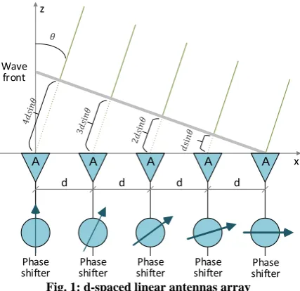
To better understand this concept let’s consider the case of a linear antennas array composed by means of 𝑑-spaced ele-ment placed as shown in Fig. 1; assuming the source is in far field also in this case, 𝐴𝐹 can be easily calculated and it’s equal to:
𝐴𝐹 𝜃 = 𝑁−1𝑛 =0𝐶𝑛𝑒𝑗𝑛𝛽𝑑𝑠𝑒𝑛 𝜃 (2)
International Journal of Computer Applications (0975 – 8887) Volume 179 – No.52, June 2018
x z
Wave front
d d
d d
Phase
shifter shifterPhase shifterPhase shifterPhase shifterPhase
A A A A A
Fig. 1: d-spaced linear antennas array
[image:2.595.61.275.75.282.2]In order to satisfy particular requirements related to antenna radiation pattern, we can also modify the amplitude of the ex-citations element. For example, we could obtain a secant radi-ation pattern suitable for a SAR applicradi-ation, using an algo-rithm based on iterated projections [3] as shown in Fig. 2.
Fig. 2: Secant radiation pattern
A similar reasoning can be made in the case of radiating ele-ments in transmission. In any case, a system able to control phase shift and amplitude of the signals related to the radiat-ing elements is necessary. This control could also be used to compensate the mutual coupling for the elements of the array.
More generally, a phased array can be equipped with a certain number of T/R modules, one for each of the radiating ele-ments, that allow to introduce attenuation and phase shifts even separately for the receiving and transmitting branches (full phased array). In fact, these modules include variable attenuators and phase shifters which can be configured using external signals to create a particular radiation pattern.
To generate the above configuration signals a system, a Beam Steering Controller (BSC), shall be used. In the following we propose two different architectures for the BSC, assuming to use digital signals to configure attenuators and phase shifters, directly or by digital-to-analog converters.
3.
BSC ARCHITECTURES
Depending on the application a BSC could have to deal with a large number of T/R modules of an antennas array. Let’s
con-sider an array with p elements placed on n rows with m ele-ments for each row and supposing to have p T/R modules with different attenuators and phase shifters for the transmit-ting and the receiving branch, to use q signals to control each attenuator, r signals to control each phase shifter and u signals to enable separately the receiving and transmitting branches for each T/R module. Assuming to use an architecture with parallel interfacing for attenuators and phase sifters, we can calculate the number s of control signals necessary to imple-ment the electronical beam steering for a generic configura-tion of the antennas array using the following formula.
𝑠 = 2𝑝 𝑞 + 𝑟 + 𝑝𝑢 = 2𝑛𝑚 𝑞 + 𝑟 + 𝑛𝑚𝑢 (3)
This architecture maximizes the performance in terms of time employed to pass from a pointing angle to another one but it requires a big quantity of signals to be generated. For exam-ple, if we consider a phased array of 200 radiating elements, using 12bit lines to configure each attenuator (𝑞 = 12), 12bit lines to configure each phase shifters (𝑟 = 12) and two signal to enable/disable the receiving and transmitting branches (𝑢 = 2), we need a BSC with 5200 output configuration sig-nals. Therefore, this solution involves the use of a Distributed BSC having a distributed architecture that spreads out over several nodes the significant number of output configuration signals to be managed.
A second architectural solution, less expensive and easier to implement, provides, instead, the use of a concentrated Beam Steering Controller, consisting of a single node that interfaces with all the T/R modules of the phased array by means of cer-tain number of point-to-multipoint buses connected to the T/R modules. In particular, each bus can be connected with all the T/R modules located on a raw of the phased array in a daisy-chain configuration so as to minimize the number of signals needed to program phase shifters and attenuators. Obviously, in this case attenuators and phase shifters (or the related digi-tal-to-analog converters) shall be equipped with a serial inter-face able to receive the configuration settings.
The above two architectural solutions are described below.
3.1
Distributed BSC Architecture
The Distributed Beam Steering Controller (D-BSC) architec-ture is composed by means of a Primary Distribution Node (PDN) and a certain number of Derivative Distribution Nodes (DDN) as shown in Fig. 3.
Prim ary Dis tribution Node
Deriva tive Dis tribution
Node #1 ... Azimuth an d E levatio n
Gen eral System Clo ck
Configuration Se ttings
Deriva tive Dis tribution
Node #N
Azimuth an d Elevation
Fig. 3: Simplified Architecture of a Distribuited BSC
[image:2.595.68.270.348.516.2]International Journal of Computer Applications (0975 – 8887) Volume 179 – No.52, June 2018
3.1.1
Primary Distribution Node
PDN is a controller node equipped with an interface able to communicate with DDNs on a point-multipoint bus. This con-troller generates and distributes the above general system clock signal to DDNs to synchronize all the operations, rece-ives from a dedicated data interface the desired beam angular position for the beam in terms of azimuth and elevation an-gles, encodes on a certain number of bits these anan-gles, re-trieves from memory or receives from the outside (through another dedicated interface) the configuration settings for the T/R modules, encapsulates the azimuth and elevation angles, the T/R modules configuration settings and DDNs configura-tion settings in a frame with a specific protocol, and, finally, transfers the bits of this frame to the DDNs via the serial digi-tal bus using a point-to-multipoint connection. All the
control-ler operations described above are managed and timed by a finite state machine (FSM) implemented inside the controller. This FSM also send a Next Angle Ready signal which we will be examined later. The frequency used to transfer data on the serial communication bus and, consequently, the time neces-sary to pass from a couple of angular values for azimuth and elevation to another one (including the processing time at the DDNs) shall be compatible with the minimum time to change the beam pointing angle required by the application. The pro-posed architecture for PDN, with particular emphasis on the controller, is shown in the following figure. This architecture is well suited to an FPGA-based hardware platform imple-mentation.
Azimuth (φ)
Elevation (θ) Angles
Encoding
Serial Tra nsm iss ion Angles
Data Inte rfa ce
Sys tem Clock Generator
NDDs Reset NDDs Enable
System Clock Serial Data
Data Clock Next Angle Ready
Fra me Generation
Finite State Machine
Memory
Configuration Data Inte rfa ce T/R modules
Configuration data
[image:3.595.85.514.231.378.2]Primary Distribution Node
Fig. 4: Primary Distrubution Node architecture for D-BSC
3.1.2
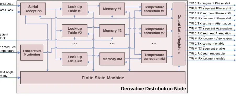
Derivative Distribution Nodes
The main task of a DDN is the conversion of the received azimuth and elevation angles values into settings for attenua-tor and phase shifters. To make this conversion a possible so-lution is to preload these settings into memory blocks for all the considered and quantized azimuth and elevation values rather than calculating these settings from time to time; in this way can obtain two advantages: a decrease of the time re-quired to switch the beam angular position from (since the time required to draw the settings contained in memory for a couple of azimuth and elevation angles is shorter than the time
it would take to perform the computation of the same settings) and a simplification of the processing executed by the DDN. Therefore this solution is adopted to design the DDN architec-ture.
The architectural scheme of a DDN is shown in the following figure for a phased array row equipped with M T/R modules.
The serial reception interface recovers the azimuth and elevation values and the configuration settings encapsulated in the serial stream sent by PDN on the point-multipoint bus.
Serial Reception
Look-up
Table #1 Memory #1
Look-up Table #2
Look-up Table #M
Memory #2
Memory #M
Finite State Machine
Ser ial Data
Data Clock
System Clock
Next Angle Ready
T/R 1 TX seg me nt Pha se shift
...
T/R 1 TX seg me nt enab le
...
T/R 1 TX seg me nt Atte nuation
...
...
...
...
...
T/R M TX segment Phase sh ift
O
u
tp
u
t L
a
tc
h
R
e
g
is
te
rs
Temperature correction #2 Temperature correction #1
Temperature correction #M
Temperature Monitoring
...
T/R modu les temperature
T/R 1 RX seg me nt Pha se shift
T/R M RX segment Phase sh ift
...
T/R M TX segment Attenu atio n
T/R 1 RX seg me nt Atte nuation
T/R M RX segment Attenu atio n
T/R M TX segment enable
T/R 1 RX seg me nt ena ble
T/R M RX segment enable
Derivative Distribution Node
Fig. 5: Derivative Distrubution Node architecture for D-BSC
The look-up tables select the correct memory location containing the attenuation and phase shift settings for a given T/R module based on the received azimuth and elevation angles. These settings are first modified taking into account
[image:3.595.76.527.522.706.2]latch registers. The above temperature is acquired by a dedicated monitoring block.
The finite state machine of the DDN has the task of managing and timing all the operations described above using the input general system clock. In particular, in order to assign a new angle to the beam at a given instant, all the attenuators and phase shifter shall be simultaneously controlled; this is accomplished by the finite state machines of DDNs on the basis of the signal, named Next Angle Ready, provided by the NDP. Furthermore, this finite state machine also interprets the configuration settings received through the serial stream, carrying out the consequent operations, such as, for example, the activation/deactivation of the transmitting and receiving segments of the T/R modules.
Given the number of signals to be managed, the high paral-lelism required for the simultaneous management of all the T/R modules belonging to the same row and the need to pro-vide blocks of memory to be used to preload the settings for attenuators and phase shifters according to the azimuth and elevation angles, a possible solution to implement the DDN architecture could require a certain number of slave FPGAs, each one dedicated to a certain number of T/R modules, coor-dinated by a master FPGA, having substantially the task of redistributing the signals received from the NDP node and timing and managing, through the FSM, the operations of the slave FPGAs; the latter would only include look-up tables, memory blocks as well as the output latch registers. The num-ber of required FPGAs depends on the numnum-ber of T/R mod-ules located on a raw of the array. Only one FPGA could be used to both for the above master and slave operations when the raw of the array is equipped with few T/R modules (typi-cally less than 12 T/R modules, considering attenuation and phase shift settings spread on a 10bit parallel interfaces and a FPGA whit 600 I/Os).
An implementation of a distributed architecture using one FPGA for each T/R module of an array composed by means of 64 radiating elements is shown in [5]. Other distributed ar-chitectures can be find in [4], where each derivative node has
to manage 32 T/R modules, and in [6], where a distributed processor architecture developed on a 3 layers hierarchy is proposed.
3.2
Centralized BSC Architecture
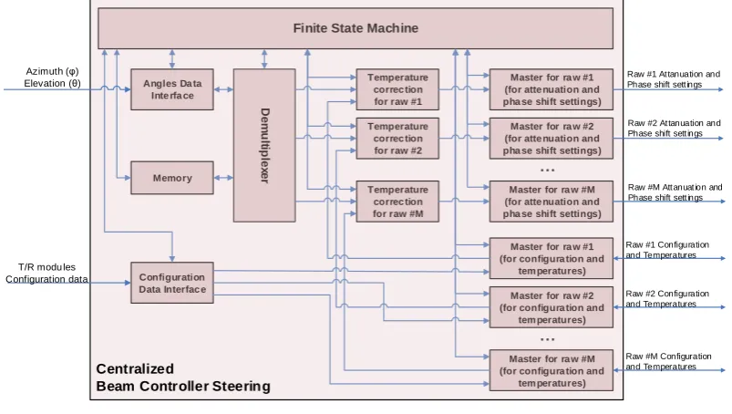
The Centralized Beam Controller Steering (C-BSC) architec-ture consists of a single node (hence the name of concentrated architecture) that receives the azimuth and elevation angles, calculates (or collects from a memory) the settings for attenu-ators and phase shifters based on the above angles, serially transfers these settings to the T/R modules, enables/disables, individually, the transmitting and / or receiving segments for each of the T/R modules belonging to the same board on the basis of information pre-loaded in memory or received from a dedicated external interface.
The C-BSC is based on the following assumption: attenuators and phase shifters of the T/R modules located on the same raw of the antennas array are equipped with a serial interface and interconnected through a daisy-chain topology to receive their settings. Using m master-slave configuration, one for each raw of the array, where the C-BSC node provides the master sending the settings and the T/R modules (of that raw) are the slaves which receive these settings, it is possible to reduce the signals of interconnection to the signals of the seri-al interface plus a data latch signseri-al used to synchronize the configuration of the all the attenuators and phase shifters.
In order to further decrease the signals to be generated, a simi-lar solution can be used also for the configuration data and the temperature monitoring of the T/R modules. In any case, for each raw of the array the interfaces used to transfer these data shall be separated from the preceding ones used for the atten-uation and phase shift settings in order to not reduce the throughput dedicated to these settings and, consequently, the time required to change the beam pointing angle.
The internal architecture of the C-BSC, arising from the above considerations, is shown in the following figure and it is re-lated to a planar antennas array composed by means of M rows.
Finite State Machine
Angles Da ta Inte rfa ce
D
e
m
u
lti
p
le
xe
r
Temperature correc tion for raw #1
Temperature correc tion for raw #2
Temperature correc tion for raw #M
Master for ra w #1 (for atte nuation and pha se shift settings)
Master for ra w #2 (for atte nuation and pha se shift settings)
Master for ra w #M (for atte nuation and pha se shift settings)
Configuration Data Interfac e
Master for ra w #1 (for configura tion and
tem peratures)
Master for ra w #2 (for configura tion and
tem peratures)
Master for ra w #M (for configura tion and
tem peratures) Memory
...
...
Centralized
Beam Controller Steering
Azimuth (φ) Elevation (θ)
T/R modu les Configuration data
Raw #1 At tanuation and Phase shift sett ings
Raw #2 At tanuation and Phase shift sett ings
Raw #M Att anuat ion and Phase shift sett ings
[image:4.595.97.499.488.715.2]Raw #M Configuration and Temperatures Raw #2 Configuration and Temperatures Raw #1 Configuration and Temperatures
Fig. 6: C-BSC architecture
This architecture use a dedicated data interface to receive azimuth and elevation angular values from an external equip-ment. An internal demultiplexer collects phase shift and
International Journal of Computer Applications (0975 – 8887) Volume 179 – No.52, June 2018
temperature of the T/R modules and sent by M blocks (one for each raw of the array) to the attenuators and phase shifter of the array T/R modules. A second data interface is used to re-ceive configuration data. These data are managed by dedicat-ed M blocks (also in this case one for each raw of the array) which sent the configuration to the T/R modules and receive the related temperatures. All the described operations are ma-naged by finite-state machine which define the timing of all the operations and provides the data latch signal (i.e. the next angle ready signal) to synchronize the configuration change for the attenuators and phase shifters of the overall system.
The described C-BSC can be realized using a platform equipped with a single FPGA. In fact, the necessary I/O re-sources are easily provided by a single commercial off-the-shelf FPGA and also the implementation on a such device should not present particular problems. The only exception is the memory: considering the capacity required by this block, it could be necessary using more than one memory banks ex-ternal to the FPGA in which to preload the values used to set the attenuators and phase shifters of the phased array system.
3.3
Architectures Comparison
Comparing the shown architectures, we can note that the distributed architecture is advantageous because the time required for configuring attenuators and phase shifters is low, since almost all operations are performed in parallel, and its implementation is scalable, since adding a derived node (and, therefore, further T/R modules to be managed) does not imply any changes to either the primary node or the other derived nodes already present (in any case the fan-out of the bus and signals between PDN and DDNs shall be evaluated). However, it is characterized by a high complexity of implementation, both in terms of the number of logical resources to be used (for example the number of required FPGAs) and in terms of the routing of the signals to be exchanged between the BSC and each row of the phase array. As a result this architecture requires high costs.
On the other hand, the concentrated architecture has lower performance (more time required to configure attenuators and phase shifters) and a reduced system scalability but it shows an implementation with simplified routing (fewer signals shall be routed) and require less logical resources.
Based on these considerations a C-BSC has been implemented within the project TELEMACO.
4.
C-BSC IMPLEMENTATION
In this section we show a C-BSC implementation focused only on the section related to the setting of the attenuators and
the phase shifters of the system, that is we don’t consider the section related to the T/R modules configuration and to the related temperature monitoring. Consequently, T/R modules temperatures are considered as an input for the system.
The implementation, named Attenuators and Shifters Controller (ASC), is based on the following assumptions:
the phased array consists of M row each equipped with an electronic board (named card) with N T/R modules, so there are 2N attenuators and 2N phase shifters;
angular data (azimuth and elevation) area received by an SPI interface;
the number of T/R modules can be different from a card to another one;
the T/R modules are voltage controlled and so, in order to digitally change the control voltage, DAC components are used;
DACs are organized by chips, each one groups L DACs;
chips are connected in a daisy-chain configuration by SPI bus, so the attenuation and the phase shift are programmed by digital data that can be serially transmitted on the above bus.
Scalability degree has been improved by a scalable design approach of the architecture, i.e. by a parameterized HDL coding of the architecture, at a cost of a major design effort.
4.1
Attenuators and Shifters Controller
The hardware architecture is depicted in Fig. 7; it is based on a Xilinx FPGA and consists of:
a Xilinx Microblaze soft-processor and its peripherals,
a Xilinx IP Core for RAM Controller,
an SPI interface, working as slave, used to receive the azimuth and elevation angles values,
a Custom IP Core, named Attenuator and Shifter Interface (ASI), for SPI programming of M cards,
a RAM memory arranged as a Look-Up-Table in which all the possible configuration values are stored for each at-tenuator and shifter of the antenna system,
Instructions LMB Bus
Data LMB Bus
BRAM DDR3 RAM
Controller
Instructions BRAM Controller
Data BRAM Controller
GPIO
R
A
M
Microblaze AXI Bus
data_in[23:0]
. . .
ASC
FSL
In
te
rfa
ce
ASI
UART
AXI Lite Bus
FSL Bus
Clock Generator
System Reset
data_valid
Tem
p
er
at
u
re
ad
ju
st
RESET
power_on_ready
C
o
n
fig
_
rea
d
y
C
LK
_
D
eb
u
g
Card #1 SPI bus signals SCLK_1
NOT_SYNC_1
MOSI_1
LDAC_1
Card #2 SPI bus signals SCLK_2
NOT_SYNC_2
MOSI_2
LDAC_2
Card #N SPI bus signals SCLK_N
NOT_SYNC_N
MOSI_N
LDAC_N
Tx
Rx
SPI Bus Slave MISO
MOSI SCLK CS Angular
Data
N
O
T
_
LD
A
C
_
in
ac
[image:6.595.64.538.75.282.2]k
Fig. 7: Attenuators and Shifters Controller (ASC)
Depending on the angular data received on the input SPI bus, the processor reads the configuration voltages from the RAM memory and send it to the ASI IP core through FSL bus.
The Attenuator and Shifter Interface is a custom IP Core de-signed to send the configuration values for attenuators and phase shifters on the SPI buses, one for each card of the an-tenna system. In particular, the ASI module executes the fol-lowing operations, organized in two phases. In the first phase (Phase 1), at power on of the system, ASI execute the initial setting of the DACs that control attenuators and shifters. In
the second phase (Phase 2), at incoming of new angular data, ASI receives through the FSL bus the configuration data for all the attenuators and the shifters, adjusts the configuration values according to the cards temperature thanks to the cor-rection parameter transmitted by the AMC unit and, then, de-multiplex and transmitted temperature compensated values on the SPI buses.
4.1.1
ASI IP core architecture
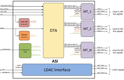
The architecture of the ASI IP Core is represented in the fol-lowing figure.
DTA
Configuration Logic Reset Interface data_in[23:0]
. . .
ASI
data_valid
CLK SPI Generator
Temp Adjust Values MET_demux_data_1
MET_demux_data_valid_1
MT_1
RESET CLK CLK_SPI
config_flag_1
MET_demux_data_2 MET_demux_data_valid_2
MT_2
RESETCLK CLK_SPI
config_flag_2
MET_demux_data_N MET_demux_data_valid_N
MT_N
Card #N SPIbus signals
SCLK_N NOT_SYNC_N MOSI_N RESET
CLK CLK_SPI
config_flag_N
CLK_SPI
RESET
CLK
RESET
config_flag_0
config_flag_1
. . .
Config status
LDAC Interface
acknot_ldac_in
NOT_LDAC_1
Card #2 SPI bus signals
SCLK_2 NOT_SYNC_2 MOSI_2
Card #1 SPI bus signals
SCLK_1 NOT_SYNC_1 MOSI_1
NOT_LDAC_2
NOT_LDAC_N . . . CLK
RESET
co nfig_flag_N
LDAC signals
Fig. 8: ASI IP Core
The architecture consists of these units:
a. DTA, Demultiplex and Temperature Adjustment module,
b. MT, Memorize and Transmit blocks, one for each card of the antenna system,
[image:6.595.79.514.430.710.2]International Journal of Computer Applications (0975 – 8887) Volume 179 – No.52, June 2018
e. Reset interface, f. LDAC Interface.
The DTA module implements the temperature compensation and the demultiplexing of the adjusted configuration values to the MT blocks. The Microblaze processor sequentially write on the FSL bus the configuration values of all the attenuators and shifters for all the cards of the antenna system. These val-ues are read and temperature compensated by the DTA and then routed to the MT blocks. The temperature correction fac-tors are received as input by an external system.
The MT block, one for each card of the antenna system, is composed by:
1. a memory unit, 2. an SPI driver, 3. a Control Logic.
The last one element implements a Finite State Machine that articulates the two phases of operations of the ASI unit and synchronizes the other elements of the module.
The memory unit consists of two kind of memories: a dual port RAM and a ROM. In this one, the settings of DAC chips that control the attenuators and the shifters are stored. This data is used during the phase 1 of the ASI operations. The dual port RAM acts as a buffer for two clock domains, the first one for the FSL bus and the second one for the SPI driv-er. In this architecture the FSL bus works at 100 MHz while the SPI transfer rate is programmable. The depth of the RAM is equal to the number of DAC chips that control the attenua-tors and shifters of the T/R modules. We also supposed that the angular data for the Transmit and Receive modules are identical, that is the radiation pattern is the same in both transmit and receive mode.
The SPI driver implements the attenuator and shifter DACs SPI protocol (an Analog Devices AD5754 DAC chip is consi-dered). The configuration values are sequentially read from ROM in phase 1 and from RAM in phase 2 and are packed in a control frame as defined in the DAC SPI protocol. Then the frame is serialized and transmitted on the 3-wire SPI bus. This operation is continuously repeated for each DAC chip on-board.
When all the DAC chips aboard of the cards of the antenna system are configured for the present angular data, the LDAC interface waits for an external strobe signal. When this signal arrives, the LDAC activates the latch signal for each card and it allows the DACs to output the desired voltage values and so to perform the change of the radiation pattern of the antenna system.
The Reset Interface handles the reset of the subsystems of the ASI IP-core.
The configuration logic outputs the state of the operations.
4.1.2
ASI IP Core implementation
The ASI core has been designed with VHDL in Xilinx ISE 14.7 software. The architecture is scalable so that the number of cards is programmable as well as the number of attenuators and shifters (DAC chips) for each card. The SPI bus frequen-cy depends on the chosen DAC chip and it is programmable. The target FPGA chosen in this work is a Virtex-6 vlx240t aboard of the ML605 Xilinx evaluation card.
A configuration of 16 cards with a total of 168 T/R modules has been considered for the testbench of the IP Core. It has been supposed that each T/R module needs to be controlled by
3 voltages, one for the attenuator and two for the shifter. The resource utilization is showed in the following table:
Table 1. Resources utilization for ASI core
Resources Utilized Available %
Occupied Slices 954 37,680 2%
Slice Registers 2,209 301,440 1%
Slice LUTs 1,831 150,720 1%
RAMB18E1/FIFO18E1s 33 832 3%
The IP Core maximum frequency is 100 MHz, as the working frequency of the FSL bus.
The minimum interval of time required to set a new pointing angle for the beam, i.e. to change the antenna pattern, depends on the number of elements and on the SPI bus frequency. The IP Core has been simulated with the above configuration and considering an SPI bus frequency of 25 MHz. The time neces-sary for the transmission of all the voltage values is of 84.73 us. At this interval of time must be added the time for the re-ceiving of the angular data on the input SPI bus and the trans-fer time of the voltage values from the external memory to the ASI core.
4.2
System Verification
The ASI Core has been integrated into the architecture of the ASC. A driver for the Microblaze Processor handles the fol-lowing operations:
external RAM initialization with all possible voltage values,
setting of the ASI IP core,
reading of the angular data on the input SPI bus,
transferring data from external RAM to the ASI IP Core,
visualization of the system status on terminal.
In order to test the behavior of the system in a laboratory envi-ronment a hardware test has been carried out.
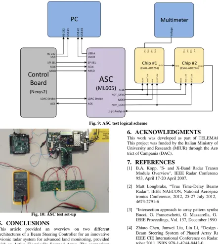
A control board (CB) has been developed to transfer the angu-lar data to the ASC as well as two evaluation boards with DAC chips aboard to verify the correctness of the SPI trans-fer. The scheme of the hardware test is depicted below.
The Control Board is a FPGA-based Digilent Nexys2 Evaluation board. A system based on Microblaze processor has been developed to handle the SPI transfer of the angular data. Both the CB and the ASC communicate with a PC in order to control the hardware test. The ASC integrates also a Logic Analyzer to acquire the signals of the SPI bus chain from the DAC chips and to verify the success of the communication between the ASC and the DACs as well as to measure the time required for the transmission.
Despite the usage of only two DAC chips, the success of the communication can be verified because of the chain scheme of the transfer. The DAC evaluation boards can be connected to only one of the 16 SPI bus outputs of the ASC on the ML605 board but the connection can be changed to test all the outputs bus in different test sessions.
Control
Board
(Nexys2)
ASC
(ML605)
SCLK MOSI
LDAC Strobe
ACK
Logic Analyz er SCLK
MISO SPI SEL
ACK
LDAC Strobe SPI SEL
PC
U
S
B
#
1
USB
U
S
B
#
2
U
SB
#
3
RS
-232
RS-232 USB A
USB B
Chip #1
(EVAL-AD5754)
SCLK NOT_SYNC MOSI
NOT_LDAC
Chip #2
(EVAL-AD5754)
M
O
S
I
N
O
T
_
SY
N
C SDIN
N
O
T
_
LD
A
C
SD OU T SD IN SD OU T
M
O
S
I
N
O
T
_
SY
N
C
N
O
T
_
LD
A
C
C
h
A
C
h
C
C
h
D
C
h
B
C
h
A
C
h
C
C
h
D
C
h
B
Multimeter
V
ol
ta
[image:8.595.58.500.88.584.2]ge
Fig. 9: ASC test logical scheme
Fig. 10: ASC test set-up
5.
CONCLUSIONS
This article provided an overview on two different architectures of a Beam Steering Controller for an innovative avionic radar system for advanced land monitoring, provided with an Active Electrically Scanned Array. The comparison between a distributed architecture and a centralized one, showed the trade-off between scalability, speed, routing complexity and costs of a Beam Steering Controller. A centralized architecture has been chosen for a hardware implementation on a FPGA based hardware platform, thanks to its benefit in terms of costs of the entire system and reduced routing complexity. A certain level of scalability degree has been obtained by scalable hardware design of the architecture at a cost of a major design effort. Finally, a test-bed solution for the implemented C-BSC is described. This implementation will be integrated into an innovative avionic radar system for advanced land monitoring developed in the framework of TELAMACO project.
6.
ACKNOWLEDGMENTS
This work was developed as part of TELEMACO project. This project was funded by the Italian Ministry of Education, University and Research (MIUR) through the Aerospace Dis-trict of Campania (DAC).
7.
REFERENCES
[1] B.A. Kopp, ''S- and X-Band Radar Transmit/Receiver Module Overview'', IEEE Radar Conference, pp. 948-953, April 17-20 April 2007.
[2] Matt Longbrake, “True Time-Delay Beamsteering for Radar”, IEEE NAECON, National Aerospace and Elec-tronics Conference, 2012, 25-27 July 2012, ISB 978-1-4673-2791-6
[3] “Intersection approach to array pattern synthesis”, O. M. Bucci, G. Franceschetti, G. Mazzarella, G. Panariello, IEEE Proceedings, Vol. 137, December 1990
[4] Zhiato Chen, Junwei Liu, Lin Li, “Design of Scalable Beam Steering System of Phased Array Radar”, 2011 IEEE CIE International Conference on Radar, 24-27 Oc-tober 2011, ISBN 978-1-4244-8443-0
[5] Rafael H. Medina Sanchez , “Beam steering control sys-tem for low-cost phased array weather radars: design and calibration techniques”, Doctoral Dissertations, Universi-ty of Massachusetts, 2014