Design and Analysis of Different Types of Combinational
Circuit using Reversible Gate
Reena Mannewar
M. Tech. Scholar Department of EC SISTec, Gandhi Nagar, Bhopal
Pankaj Kumar Vyas
Assistant Professor Department of EC SISTec, Gandhi Nagar, Bhopal
Paresh Rawat, PhD
Head of Dept. Department of EC SISTec, Gandhi Nagar, Bhopal
ABSTRAC
T
Most traditional computers lose information during the process of computation. Reversible computation is different from the traditional computation in that it preserves information while manipulating it. Energy dissipation is proportional to the number of bits lost during computation. Power dissipation can be negligible if overall design consisting of reversible logic only. The area of reversible logic has received great importance in recent years because of its beneficial feature of reduction in power dissipation. In this design different types of combinational circuit i.e. reversible multiplexer (RM), reversible de-multiplexer (RDM), reversible encoder (RE) and reversible decoder (RD). This paper represents the new methods and approaches to implement the components of the processor and modified design is to utilize advantages of existing techniques and at the same time overcoming drawbacks.
Keywords
CMOS Technology, Reversible Gate, Multiplexer, Encoder
1.
INTRODUCTION
[image:1.595.318.512.221.300.2]A gate is considered to be irreversible if the input and output vectors are not uniquely retrievable. Due to this there will be rapid internal power dissipation. It was proved by Landauer [1] that the computer must dissipate at least KTln2 of energy for each bit of information it writes or erases. An example of an irreversible gate is show in Fig. 1.
Fig. 1: Irreversible Gate
The inputs to the irreversible gate are I1, I2 …. IN. The output of the gate is output. Since the number of input vectors cannot be recovered from output vector the information will be lost.
[image:1.595.320.546.487.561.2]In order to overcome the above drawback said by Landauer, Bennet [2] proposed a logic called Reversible logic where the input and output vectors are uniquely retrievable. Reversible gates are circuits in which the number of outputs is equal to the number of inputs and there is one to one correspondence between the input and the output vectors. An example of the reversible gate is shown in the Fig. 2
Fig. 2: Reversible Gate
2.
PREVIOUS WORK
Combinational circuit is a circuit which we combine we combine the different gates in the circuit, for example encoder, decoder, multiplexer, DE multiplexer. Some of the characteristics of the combinational circuits are as follows:
1) The output of the combinational circuits at any instant of time depends on the levels present at the input terminals.
2) The combinational circuits do not have any memory. The previous state of the input does not have any effect on the present state of the circuit.
[image:1.595.60.287.535.618.2]3) The combinational circuits have n number of inputs and m number of outputs.
Fig. 3: Combinational Reversible Gate
30 more power dissipation claims that this design is not an
effective approach.
In L. Gopal et al. introduces two reversible gates namely R-I gate and R-II gate for implementation of the multiplexer. These two gates can be used for the realization of 2 to 1 multiplexer and even vice versa without using any extra circuitry. The advantage of these gates is that they require minimal hardware with minimum garbage count and also can be used as data copier. Using the principle of reversibility, these two new gates realizes the logical function such as AND, XOR, MUX, DE-MUX, half adder and much more with minimum garbage count. A combinational circuit with low garbage count encourages the application of implemented gates for future aspects of low power devices. Vanadna illustrates an optimized 8:1 multiplexer design using a combinational of available reversible logic, which requires three selection lines and 8 input lines. Multiplexers are in general used for the translation of parallel data line into serial one. Here, planning of 8:1 multiplexer designed circuit uses TKS and VSMT gate for implementation. In realization of this design, all the signals are applied to the inputs of TKS gate, whereas the left out selection lines are applied to VSMT gate. Construction of overall reversible circuitry requires a total number of three reversible gates gives out 11 garbage output. The design is optimized in terms of a number of gates used in circuit and garbage output. It can be extended to accomplish numerous functions for reversible circuits.
3.
PROPOSED METHODOLOGY
Combinational circuits, in which output depend on the current state of the input includes circuit like decoder, encoder, Multiplexer, DE multiplexer, and comparator etc. Sequential circuit elements are those depends on a current state of input and previous state of the input. For example, Flip-flop, latches, counter and shift registers. Both combinational and sequential circuit are designed and implemented in a reversible manner using Verilog HDL. By considering the computational complexity, memory access pattern and complexity of instruction, which can configure the execution time of the overall algorithm.
Tool Description
In this thesis two software tool Xilinx 14.1 versions are used for analyzing and the simulation of the circuits. Synthesis is done in 14.1i version also for the proposed designs. Xilinx 14.1i software version is used for checking simulation result with Virtex-4 generation offers the choice of platform, each delivers the cost optimized for programmable logic and used for low power application.
Proposed Reversible Multiplexer
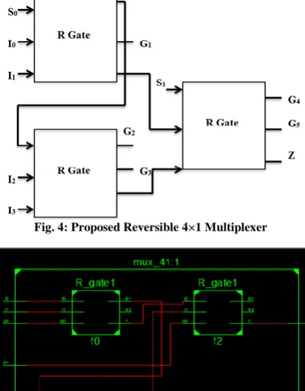
The multiplexer (MUX) is a device, which picks any one of many input signals and forwards the selected input to a single output line. The main use of multiplexer is for data selection, translation of parallel data into serial one. Circuit implementation for the 4_to_1 multiplexer is shown in Fig. 4 is done in a reversible manner by using reversible logic R gate. The proposed design consisting of two selection lines S0 and S1, our input signal of the multiplexer are I0, I1, I2, I3, and Z as output line utilizes a total of three R gates for implementation. The output equation for 4:1 multiplexer can be given as: Z =
[image:2.595.317.539.80.365.2]S1’S0’I0,+ S1’ S0 I1 + S1 S0’ I2 + S1 S0 I3.
[image:2.595.315.551.250.439.2]Fig. 4: Proposed Reversible 4×1 Multiplexer
Fig. 5: RTL View of Reversible 4×1 Multiplexer
Fig. 6: VHDL Text Bench of Reversible 4×1 Multiplexer
[image:2.595.313.547.463.575.2] [image:2.595.331.526.602.694.2]Fig. 8: RTL View of Reversible 2×1 Multiplexer
Fig. 9: VHDL Text Bench of Reversible 2×1 Multiplexer
Proposed Reversible De-multiplexer
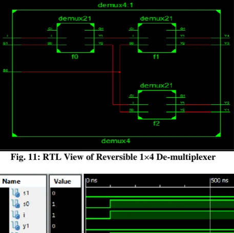
[image:3.595.316.545.77.305.2]Conversely, a DE multiplexer (DEMUX) is a device which takes a single input signal and selecting one of the many data output lines, which are connected to a single input. It is nothing just the reverse operation of multiplexing. Proposed design implementation for 1:4 reversible de-mux is done by using three reversible R gates is shown in Fig. 10. The design consisting of two selection lines, one single input I and four outputs Z0, Z1, Z2, Z3. The logical expression for the output of 1:4 demux are as follows: Z0 = I S1 S0, Z1 = I S1 S0‘, Z2 = I S1 ‘ S0 and Z3 = I S1’ S0’.
Fig. 10: Proposed Reversible 1×4 De-Multiplexer
Fig. 11: RTL View of Reversible 1×4 De-multiplexer
Fig. 12: VHDL Text Bench of Reversible 1×4 De-multiplexer
Proposed Reversible Decoder
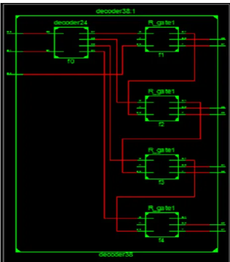
[image:3.595.64.275.498.675.2]Proposed 3:8 reversible decoder is built by using 2:4 reversible decoder, which was implemented by using HL gate and four R gates is shown in Fig. 13. Proposed reversible 3:8 decoder consisting of two inputs (A, B, C) and eight outputs i.e., Yi (i = 0, 1... 7). The output equations for 3:8 decoder is given by following expressions: Y0 = A'B'C', Y1 = A'B'C, Y2 = A’BC’, Y3 = A’BC, Y4 = AB’C’, Y5 = AB’C,Y6 = ABC’, Y7 = ABC. Our proposed approach achieves the better improvements in terms of design parameters such as gate count, quantum cost, garbage output, constant input and total cost as compared to same criteria with existing approaches.
[image:3.595.313.532.500.679.2]32 Fig. 14: RTL View of Reversible 3×8 Decoder
Fig. 15: VHDL Text Bench of Reversible 3×8 Decoder
4.
SIMULAATION RESULT
More specifically, we have developed new garbage-free circuits for addition and are working towards a general multiplication circuit. We have also combined multiple operations together to implement a reversible arithmetic logic unit. With these and other garbage-free arithmetic circuits it is possible to design larger reversible computing systems.
Reversible Gate Parameter:-
Gate Count (GC): The number of gates used to realize reversible circuit
Garbage Outputs (GO): The number of unused outputs in a reversible logic. The inputs regenerated at the outputs are not garbage outputs.
Ancilla Inputs (AI): The number of input kept constant at either 0 or 1.
Delay : It corresponds to number of primitive quantum gates in the critical path of the circuit.
[image:4.595.53.287.368.494.2]Quantum Cost:- Quantum cost is defined, as the number of basic quantum gates like controlled-NOT, Controlled V+, Controlled V and NOT gate.
Table 1: Comparative Study of Parameters for Reversible Components
Reversible Designs Quantum Cost Garbage Output Constant Input Gate Count Power Reversible Multiplexer
Existing 15 5 0 21 2135.4
Proposed 12 5 0 12 1707.6
Reversible DEMUX
Existing 15 2 3 21 2135.4
Proposed 12 2 3 12 1707.6
Reversible Decoder
Existing 27 1 6 35 4126.7
Proposed 23 1 6 23 3557.5
Reversible Encoder
Existing 27 9 4 35 4126.7
Proposed 22 9 4 22 3130.5
5.
CONCLUSION
As we realize that the rudiments of reversible figuring depend on the relationship between entropy, heat move between atoms in a framework, the likelihood of a quantum molecule possessing a specific state at any given time, and the quantum electrodynamics between electrons when they are in close nearness.
Hence in this design we have proposed a design to calculate the power that is analogous to heat dissipation and to compare the delay and increase the number of logical arithmetic operation.
6.
REFERENCES
[1] Gopi Chand Naguboina and K. Anusudha, “Design and Synthesis of Combinational Circuits Using Reversible Decoder in Xilinx”, IEEE International Conference on Computer, Communication, and Signal Processing (ICCCSP-2017).
[2] Marcin Bryk , Krzysztof Gracki , Paweł Kerntopf , Marek Pawłowski , Andrzej Skorupski, “Encryption using reconfigurable reversible logic gate and its simulation in FPGAs”, Mixed Design of Integrated Circuits and Systems, 2016 MIXDES - 23rd International Conference IEEE Xplore: 04 August 2016.
[3] Umesh kumar , Lavisha Sahu, Uma Sharma, “Performance Evaluation of Reversible Logic Gates”, International Conference on ICT in Business Industry & Government (ICTBIG), IEEE 2016.
[4] Lafifa Jamal and Hafiz Md. Hasan Babu, “Design and Implementation of a Reversible Central Processing Unit”, IEEE Computer Society Annual Symposium on VLSI, 2015.
[5] Junchaw Wing and Ken Choi, “A Carry look ahead adder designed by reversible logic”, SOC Design Conference (ISOCC), International Conference on
IEEE 2015.
[6] D. Grobe, R. Wille, G.W. Dueck, and R. Drechsler, “Exact multiple control Toffoli network synthesis with sat techniques”, IEEE Transaction on CAD, 2014.
[8] V. V. Shende, A.K. Prasad, I.L. Markov, and J.P. Hayes, “Synthesis of reversible logic circuits”, IEEE Transaction on CAD, Vol. 22, Issue 10, Oct. 2012.
[9] D. Grbe, R. Wille, G. W. Dueck, and R. Drechsler, “Exact synthesis of elementary quantum gate circuits for reversible functions with dont cares”, in Process of the International Symposia on Multi-Valued Logic, pages 214–219, Dallas, Texas, May 2012.
[10] Madhusmita Mahapatro, Sisira kanta Panda and Jagannath Satpathy, “Design of Arithmetic Circuits Using Reversible Logic Gates and Power Dissipation Calculation”, Electronic System Design (ISED), International Symposium on electronic system design, 2011.