COMPARATIVE STUDY OF DIFFERENT TECHNOLOGIES TO REPLACE CMOS TECHNOLOGY
*,
1
PhD Scholar of RVCE, Department
2Associate Professor,
ARTICLE INFO ABSTRACT
This paper discuss about Survey done for the digital circuit design using different VLSI technologies. In digital electronic world, delay and power consumption improvement are the most important performance parameters of a circuit. To achieve this goal, we
complementary metal oxide semiconductor (CMOS) technology, reducing the channel length below about 45nm leads to critical problems and challenges such as decreasing gate control, short channel effect, high pow
increment. For these reasons reducing the transistors size finally will stop at a point, leading grabbing advantage of new technologies that helps to overcome above proble
was conducted to replace CMOS technology and technology with a suitable technology.
Copyright©2017, Anitha and Dr. Srividya. This is an open use, distribution, and reproduction in any medium, provided
INTRODUCTION
Scaling down of electronic devices has been the basic approach for improving the performance of
Scale Integrated Circuits (ULSIs). Metal Oxide Semiconductor Field Effect Transistors (MOSFET) have been the most widespread electron devices for ULSI applications and hence reducing the sizes of MOSFET has been the basis of the development of the semiconductor industry.
CMOSFET is entering into nano scaled method. Fundamental limits of CMOSFETs and technological challenges with respect to the scaling of CMOSFETs are encountered. To overcome challenges, that are encountered by CMOSFETs the new technologies such as benzene rings, Quantum
automata (QCA), single electron transistor (SET), carbon nanotube technology and others have risen up. They are all used to construct the circuits such as resonant tunnelling rectifying diode, molecular diode, N input logic gates, tunnelling based static Random Access Memory
full adder, ring counter, T-FF, charge sensor, ultra
microwave detector, super sensitive electrometer, single electron spectroscopy, quantum computer, programmable single electron transistor and many more.
*Corresponding author: Anitha, N.
PhD Scholar of RVCE, Department of ECE, Asst. Prof. at AIeMS, Bidadi, India
ISSN: 0975-833X
Article History: Received 19th June, 2017
Received in revised form 27th July, 2017
Accepted 15th August, 2017
Published online 30th September, 2017
Citation: Anitha, N. and Dr. Srividya, P. 2017. “
Current Research, 9, (09), 58019-58035.
Available
Key words:
CNFET, CMOS, QCA, SET, Molecular Electronics, Ring counter, TSRAM, T-FF, Benzene Ring.
RESEARCH ARTICLE
COMPARATIVE STUDY OF DIFFERENT TECHNOLOGIES TO REPLACE CMOS TECHNOLOGY
*,1
Anitha, N. and
2Dr. Srividya, P.
PhD Scholar of RVCE, Department of ECE, Asst. Prof. at AIeMS, Bidadi, India
Associate Professor, Department of ECE, RVCE, Bangalore, India
ABSTRACT
This paper discuss about Survey done for the digital circuit design using different VLSI technologies. In digital electronic world, delay and power consumption improvement are the most important performance parameters of a circuit. To achieve this goal, we can reduce scaling of the feature size. In complementary metal oxide semiconductor (CMOS) technology, reducing the channel length below about 45nm leads to critical problems and challenges such as decreasing gate control, short channel effect, high power density, high sensitivity to process variation and exponential leakage current increment. For these reasons reducing the transistors size finally will stop at a point, leading grabbing advantage of new technologies that helps to overcome above proble
was conducted to replace CMOS technology and a comparison is done to replace the CMOS technology with a suitable technology.
open access article distributed under the Creative Commons Attribution provided the original work is properly cited.
Scaling down of electronic devices has been the basic approach for improving the performance of the Ultra Large Metal Oxide Semiconductor Field Effect Transistors (MOSFET) have been the most widespread electron devices for ULSI applications and hence reducing the sizes of MOSFET has been the basis of the The scaling of the CMOSFET is entering into nano scaled method. Fundamental limits of CMOSFETs and technological challenges with respect to the scaling of CMOSFETs are encountered. To ed by CMOSFETs the new technologies such as benzene rings, Quantum-dot cellular automata (QCA), single electron transistor (SET), carbon nanotube technology and others have risen up. They are all used to construct the circuits such as resonant tunnelling diode, rectifying diode, molecular diode, N input logic gates, tunnelling based static Random Access Memory (TSRAM), FF, charge sensor, ultra-sensitive microwave detector, super sensitive electrometer, single py, quantum computer, programmable
PhD Scholar of RVCE, Department of ECE, Asst. Prof. at AIeMS, Bidadi,
Benzenering
Benzene rings (or molecular electronics) are to be true successor technology to CMOS which is used to construct Resonant tunnelling diode (Jagadesh Kumar, 2007
diode using these devices logical (or digital) circ constructed such as N input logic gates
2013), molecular diode (Paul Franzon Static Random Access Memory (TSRAM)
James C. Ellenbogen, 1999). Molecular Electron (or) Benzene ring devices are capable of enhan
response time and area. But molecules have disadvantages of being instable at high temperatures, difficulty of integrating molecules with bulk materials
Molecules operate in quantum mechanical domain. molecule scale devices are combined to form large molecular circuits, these components can't be expected to behave in the same way they do in isolation
Ellenbogen, 1999). Because of quantum wave interference and other effects that influence the molecular charge distribution, there is a charge sharing problem in molecular electronic circuits (Greg Y. Tseng and James C. Ellenbogen, 1999 to this stability of the voltage in memory system might be difficult. As electrons travel through a molecule, some of their energy can be transferred to motions of the nuclei in the molecule such as the internal vibrations and rotations. The amount of energy transferred is dependent on how strongly the electronic energy levels of the mole
vibrational modes of the molecule
International Journal of Current Research
Vol. 9, Issue, 09, pp.58019-58035, September, 2017
“Comparative study of different technologies to replace CMOS technology
Available online at http://www.journalcra.com
z
COMPARATIVE STUDY OF DIFFERENT TECHNOLOGIES TO REPLACE CMOS TECHNOLOGY
Bidadi, India
RVCE, Bangalore, India
This paper discuss about Survey done for the digital circuit design using different VLSI technologies. In digital electronic world, delay and power consumption improvement are the most important can reduce scaling of the feature size. In complementary metal oxide semiconductor (CMOS) technology, reducing the channel length below about 45nm leads to critical problems and challenges such as decreasing gate control, short channel er density, high sensitivity to process variation and exponential leakage current increment. For these reasons reducing the transistors size finally will stop at a point, leading to grabbing advantage of new technologies that helps to overcome above problems. Hence, the survey a comparison is done to replace the CMOS
ribution License, which permits unrestricted
Benzene rings (or molecular electronics) are to be true successor technology to CMOS which is used to construct Jagadesh Kumar, 2007), Rectifying logical (or digital) circuits canbe input logic gates (Nasrollahnejad et al., Paul Franzon et al.,), tunnelling-based Static Random Access Memory (TSRAM) (Greg Y. Tseng and . Molecular Electron (or) Benzene ring devices are capable of enhancing some properties such as response time and area. But molecules have disadvantages of being instable at high temperatures, difficulty of integrating molecules with bulk materials (Paul Franzon et al., ?). Molecules operate in quantum mechanical domain. When molecule scale devices are combined to form large molecular circuits, these components can't be expected to behave in the same way they do in isolation (Greg Y. Tseng and James C. . Because of quantum wave interference and ts that influence the molecular charge distribution, there is a charge sharing problem in molecular electronic Greg Y. Tseng and James C. Ellenbogen, 1999). Due to this stability of the voltage in memory system might be ravel through a molecule, some of their energy can be transferred to motions of the nuclei in the molecule such as the internal vibrations and rotations. The amount of energy transferred is dependent on how strongly the electronic energy levels of the molecule couple to the vibrational modes of the molecule (Greg Y. Tseng and James INTERNATIONAL JOURNAL OF CURRENT RESEARCH
C. Ellenbogen, 1999). Energy dissipation is an architectural issue for any molecular memory proposal because it will diminish the effectiveness of electron transport and signal transmission through a molecular structure. In the extreme case it could lead to breaking of bonds and destruction of the device (Greg Y. Tseng and James C. Ellenbogen, 1999). Addressing individual molecular memory cells is a challenge of molecular-scale architecture (Greg Y. Tseng and James C. Ellenbogen, 1999). Benzene is a very important organic substance with the formula C6H6. The benzene molecule consists of half dozen carbon and half dozen hydrogen atoms. Six hydrogen atoms are connected to every hydrogen carbon atoms and form a ring (Wikipedia.org).
Benzene could be a natural constituent of fossil fuel and is one amongst the elementary petrochemicals. Benzene could be a colourless and extremely ignitable liquid with a sweet smell,
and is liable for the aroma around petrol stations
(Wikipedia.org). It’s used primarily as a precursor to the
manufacture of chemicals with a lot of complicated
structure, like ethyl groupbenzene and cumene, of that billions of kilograms are created. As a result of benzene incorporates a high octane rating, it’s very important part of gasoline (Wikipedia.org). Most non-industrial applications are restricted to use benzene as a result of it’ssombody’s matter. New molecular electronic systems, architecture and analytical tools are explored by chemist, physists and engineers. Molecular elements like switches, rectifiers, transistors and memories are currently arising. In fact, molecular physics systems are composed of molecules with specific functions. Molecular physics has some benefit over different technologies for implementing logic circuits. Several molecules have completely different geometric structures permitting distinct optical and electrical options. Additionally, tools are developed for molecular synthesis. There are 2 main molecular electronic structures used for logic design particularly polyphenylene-based chains and carbon nanotubes. However, it’s a lot of easier to design a lot of complicated logic structures using polyphenylene. Polyphenylene chain has been used as resonant tunnelling diodes, resistors and wires. Carbon nanotubes are employed in implementing logic and arithmetic circuits like full adders, FPGA switches, multiple valued logic circuits.
Polyphenylene-based components
[image:2.595.322.539.121.285.2]In this we tend to realizepolyphenylene-based parts. To realize a special practicality in logic style, foremost molecular structures as switches are build then combined them into a complex circuit.
Figure 1. Benzene ring
Polyphenylene-based conductors are composed of benzene rings with one or two hydrogen atoms eliminated. Benzene (C6H6) and its equivalent notations are illustrated in Figure 1. In Figure 2, we tend to see the phenyl and phenylene rings followed by a polyphenylene chain. We tend to get
polyphenylene by binding phenylene to every alternative on either side and terminating the result with phenyl teams. They’ll be created in several shapes and lengths. Benzene and
polyphenylenemolecules are referred to as aromatic
(Wikipedia.org).
Figure 2. Polyphenylene chain
Conductors or wires
Conjugated aromatic organic molecules. A benzene ring having the formula C6H6 is shown in Figure 3(a). A benzene ring with one in every of the hydrogenelement is removed to form C6H5in order that it will be warranted as a group to alternative molecular parts as shown in Figure 3(b). Such a ring-like substituent group is termed a “phenyl group”. By removing two hydrogens from benzene, one obtains the structure C6H4 or “phenylene”, a ring that has two free binding sites as shown in Figure 3(c). By binding phenylenesevery alternative on either side and terminating the ensuing chain-like structures with phenyl teams, one obtains a sort of molecule referred to as a “polyphenylene”. Polyphenylenes, like the upper molecular structure in Figure 3(d), could also becreated in a very variety of various shapes and lengths. Additionally, one could insert into a polyphenylene chain alternative varieties of molecularteams (e.g., singly-bonded aliphatic teams, doubly-bonded ethenylteams, and triply bonded ethynyl or “acetylenic” groups) to get “polyphenylene-based” molecules with terrible helpful structures and properties. Associated example of such a polyphenylene-based molecule is that the lower structure in Figure 3(d). Molecules like benzene and polyphenylenes, that incorporate benzene-like ring structures as vital elements, are termed “aromatic”. As mentioned shortly on top of, varied investigators recently have performed sensitive experiments during which single
polyphenylene based molecules are shown to conduct
electricity. In one example of such associate experiment, Reed associated his collaborators passed an electrical current through a monolayer of roughly 1000 polyphenylene-based molecular wires that were panoplied in a very nanometer-scale pore and adsorbate to metal contacts on either finish (Reena Monica and Sreedevi, 2014). The system was rigorously ready
specified all of molecules within the “nanopore” were identical 3 benzene-ring polyphenylene-based chain
[image:2.595.39.290.632.730.2]current corresponds to or so 200 billion electrons per second being transmitted across the short polyphenylene-based molecular wire. Whereas polyphenylene based molecular wires like those portrayed in Figure 3(d) don't carry the maximum amount current as carbon nanotubes, polyphenylenes and their derivatives are abundant smaller molecules. Thus, as a result of their terribly tiny cross sectional areas, they are doing have terribly high current densities. Approximate current densities are calculated for many chosen molecular electronic devices as well as for a typical macroscopic copper wire. Reed and his collaborators observe that the present density for an inevitable nano level problems to perform computing. It's potential benefits together with high speed, high device density and low-power dissipation.
Figure 3.a.Phenyl group (Bnezene), b. Phenyl group (benzene), c. Phenylene group (benzyne), d. Polyphenylene, e. Insulator
Diodes
Two types of diodes have been implemented via molecular electronics: rectifying diode, and resonant tunnelling diode (RTD).
Rectifying Diode
A rectifying diode is an electronic component that passes current in one direction. It's plenty of applications in planning electric circuits. The primary analysis regarding molecular electronics was supported rectifying diodes in 1974. The makes an attempt showed that the lowest unoccupied molecular orbital (LUMO) and therefore the highest occupied molecular orbital (HUMO) will be aligned in such some way that conductivity is merely possible in one direction. During this approach, constructing molecular diode is feasible. Figure 4 shows the structure of a rectifying diode. It consists of two sections S1, and S2 which is separated by an insulating cluster R.
Figure 4. Structure of a molecular diode
Figure 5. Schematic representation of a molecular diode
Molecular Resonant Tunnelling Diode
The RTD has been intensely researched in last three decades as a promising Nano electronic device for each analog and digital
application. RTDs are made-up using the semiconductor
heterostructure epitaxial techniques to appreciate the peak current-voltage characteristics that are typical of tunnel
diodes however while not the associated issues of huge
junction capacitance. The structure of a molecular resonance tunnelling diode supported a molecular conducting wire backbone is shown in figure 6. During this structure, two aliphatic methylene teams (CH2) are inserted on either side of the benzene ring. Since aliphatic teams act as insulators, they produce potential barriers to the flow of electrons within
the molecular conducting wire. The sole approach for the
current to flow within the presence of anapplied voltage is once the electrons are forced to pass through the benzene whose width is merely regarding 0.5 nm.
Figure 6. Structure of molecular resonant tunnelling diode
Figure 7. Band diagram of the molecular RTD showing the ‘OFF’ state
Monomolecular digital logicstructures
[image:3.595.57.266.226.529.2]and NOR can be constructed with the aid of aforementioned gates. The first two gates use two rectifying diodes and the last one uses one additional resonant tunnelling diode. There are also some programming techniques for designing logic circuits based on RTD. The final destination of molecular programming is to provide information processing systems at molecular levels.
1.Realization of Diode Logic Molecular ANDGate
The circuit representation of a diode logic AND gate is shown in (Fig-8) and the schematic representation of the diode logic molecular AND gate is shown in (Fig- 9). The schematic of the exemplary poly-phenylene diode logic molecular AND gate is shown in (Fig- 10)
Figure 8. Circuit diagram of the diode logic AND gate
[image:4.595.313.550.236.313.2]The molecular AND gate consists of two inputs A and B and one output C connected to the respective contacts. This structure exhibits the classical semiconductor AND gate behaviour. As shown in (Figure 8), the single molecule AND gate consists of two conducting wires each having a donating section (with at least one electron donating group)as well an accepting section (with at least one electron accepting group), and a respective insulating group R inserted between the accepting and donating sections.
Figure 9. Schematic representation of the diode logic molecular AND gate
What is important about the above molecular AND gate is that it is extremely small measuring only 3nm to 4nm in area which is at least a million times smaller than the gates realized using conventional semiconductor technology.
Figure 10. Schematic of the exemplary poly-phenylene diode logic molecular AND gate
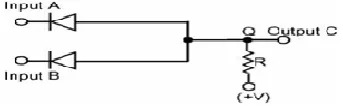
2.Realization of Molecular XOR Gate Using a Molecular RTD
[image:4.595.78.250.239.292.2]The schematic gate of the XOR gate is shown in Figure 11 and the exemplary molecular implementation of the XOR gate is shown in Figure 12. The molecular XOR gate consists of two diode-embedded molecular wires with an effective resistance R0 and their accept or sections are chemically bonded to a common connecting node. The resistance RG is made of an insulating chain. One end of RG is connected to the negative potential and the other end is connected to point Q through a conducting wire. The molecular RTD is connected between the connecting node and point Q. Another polyphenylene conducting wire is connected between point Q and the output node C of the XOR gate of which the input nodes are A and B.
[image:4.595.314.556.356.502.2]Figure 11. Circuit diagram of the diode logic XOR gate using the molecular RTD
Figure 12. Schematic representation of the diode logic molecular XOR gate using the molecular RTD
Advantages
The ability to use single molecules functioning as electronic devices has motivated researchers to minimize the size of the circuits in semiconductor industry.
Molecular electronics gives us flexibility in design such that we don't have it in traditional inorganic electronic materials.
The size of molecules is at least 1 nm and at most 100nm. This leads to less area and power dissipation. It has potential advantages including high speed, high
device density and low-power dissipation.
Disadvantages
Because of quantum mechanics and limitations of
fabrication methods, further improvements could not be achieved.
Packaging millions of silicon devices in a chip will lead to huge power consumption and expense.
[image:4.595.44.285.441.567.2]Combining individual device issue: Because molecules operate in the quantum mechanical domain, when molecular-scale devices are combined to form large molecular circuits, these components cannot be expected to behave in the same way they do in isolation.
Charge sharing: Due to the issue mentioned above regarding
combinations of individual devices, because of quantum wave interference and other effects that influence the molecular charge distribution.
Stabilization issue: A few electrons are stored on the storage node at any given time. Thus, the current from V+ to ground memory structure may be very small. If the current is too small, it may be difficult to stabilize the voltage VSN.
Mechanism of conductance: Most of these molecular
conduction mechanisms are different from those that dominate conduction in micron-scale metallic wires. This presents a significant design issue because different mechanisms may dominate at different scales (e.g., device scale vs. circuit scale).
Quantum-dot Cellular Automata (QCA)
QCA is a computing paradigm using arrays of nanostructures called quantum dots. It takes the advantages of quantum behaviour at the macroscopic scale, rather than at the atomic scale, where the quantum effects are widespread. Example of macroscopic quantum phenomena is super fluidity and super conductivity. Quantum dots are nanostructure created from semiconducting materials such as Si/Sio2. These structures can be modelled as 3-dimensional quantum wells. As a result they exhibit energy quantization effects even at distances several hundred times larger than a materials lattice constant. A quantum dot can be visualized as a well. Electrons, once trapped inside the dot, do not alone possess the required energy to escape. With the advancement of the technology the device sizes are reaching their physical limit. Hence there is a lot of research in the alternative technologies like Quantum Dot Cellular Automata. Quantum Dot cellular automata uses the position of the confined electrons in the quantum dots to represent logic states and unlike conventional electronics does not rely on electron flow. This columbic force is responsible for all the logic operations and transfer of the states from one location to another. As a replacement for CMOS technology, quantum cellular automata was proposed by Lent et al. to implement classic cellular automata with quantum dots. In order to distinguish this proposal from models of cellular automata performing quantum computation, the term has been changed to quantum-dot cellular automata (QCA). QCA is a revolutionary technology that exploits the QCA Fundamentals (Wikipedia.org)
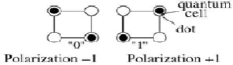
A.QCA cell
A quantum-dot cellular automata (QCA) may be a square nanostructure of electron wells confining free electrons. Each cell has four quantum dots which can hold a single electron per dot. The four dots are located at the corners of the cell and only two electrons are injected into a cell. By the clocking mechanism, the electrons can tunnel through to neighbouring cells during the clock transition by the interaction between electrons. A high potential barrier at the settled clock signal locks the state and results in a local polarization which is
determined by Coulombic repulsion. The two electrons reside in opposite corners so that two polarizations are possible as shown in Figure 13. Those two binary states can be used to make QCA cell or a storage cell, a computing cell, or a wire. The numbering of the dots (denoted as i) in the cell goes clock-wise starting from the dot on the top right: top right dot i =1, bottom right dot i =2, bottom left dot i =3 and top left dot i =4. A polarization P in a cell is defined as
[image:5.595.344.513.231.278.2]Where ρi denotes the electronic charge at dot i.
Figure 13. QCA Cell
B. Signal flow
A series of QCA cells act like a wire. A QCA “wire” is a chain of cells as shown in Figure 14, where the cells are adjacent to each other rather than a physical wire. Such a wire is used as an interconnection between all kinds of logic components. Therefore, QCA has the ability to offer “processing-in-wire”. Since no electrons tunnel between cells, QCA provides a mechanism for transferring information without current flow. An illustration of a QCA wire is shown in Figure 14. During each clock cycle half of the wire is active for signal propagation, while the other half is stable. During the next clock cycle, half of the previous active clock zone is deactivated and the remaining active zone cells trigger the newly activated cells to be polarized. Thus signals propagate from one clock zone to the next.
Figure 14. Signal Flow, a. Normal QCA Wire, b. Diagonal QCA Wire
C.QCA Clock
[image:5.595.320.549.521.669.2]low state and holds the value during the low state. The cell is released when the clock is in the low-to-high state and inactive during the high state.
Figure 15. Clock Zones
[image:6.595.59.279.230.362.2]The QCA clocking signal is used to control the signal propagation along the QCA cells arrangement. There are Four-Different Clocking Phases such as “SWITCH, HOLD, RELEASE and RELAX”.
Figure 16. Clock Phase
SWITCH: During this phase, the inter-dot barriers are slowly
raised and the computation takes place according to QCA cell arrangement.
HOLD: In this phase, the inter-dot barriers are kept high and the QCA cells retain their states.
RELEASE: During this phase, the barriers are lowered and the cells are allowed to relax to unpolarized states.
RELAX: The barriers are kept low and the cells remain in unpolarized state.
Physical Implementations of QCA
To date, a number of different implementations to realize the bistable and local interaction required by the QCA paradigm have been proposed. Both elec-trostatic interaction-based QCA implementations (metal-dot, semiconductor, and molecular) and magnetic QCAs have been investigated. A brief overview of these four distinct classes of QCA and their advantages and disadvantages follows.
1.Metal-Island QCA
The metal-island QCA cell was implemented with relatively large metal islands (about 1 micrometre in dimension) to demonstrate the concept of QCA. The dots are made of aluminium with aluminium oxide tunnel junctions between them. In this metal-island QCA cell, electrons can tunnel between dots via the tunnel junctions. These two pairs of dots are coupled to each other by capacitors. Two mobile electrons in the cell tend to occupy antipodal dots due to electrostatic repulsion. Metal-island QCA components including majority gates, binary wires, memories and clocked multistage shift registers have been fabricated. The operating temperature for metal-island QCA is extremely low, in the range of milli
Kelvin, to achieve the appropriate electron filling. This prevents the construction of complex QCA circuits running at room temperature. Therefore, the metal-island implementation is not currently seen to be a practical approach for future QCA systems.
2.Semiconductor QCA
A semiconductor QCA cell is composed of four quantum dots manufactured from standard semiconductive materials. A device was fabricated using a GaAs/AlGa. As heterostructure with a high-mobility two-dimensional electron gas below the surface. Four dots are defined by means of metallic surface gates. The cell consists of two double Quantum-Dot systems (half cells). Half cells are capacitively coupled. The charge position is used to represent binary information and the Quantum-Dot interactions are dependent on electro-static coupling. A semiconductor implementation promises the possibility of fabricating QCA devices with the advanced fabrication processes used for existing CMOS technology. However, current semiconductor processes cannot provide mass production with the ultra small feature sizes required by QCA technology. To date, most QCA device prototypes have been demonstrated with semiconductor implementations. Hence, the research presented in this book is conducted based on semiconductor QCA. However, the conclusions drawn from the research based on semiconductor implementation are applicable to other implementation types.
3.Molecular QCA
A molecular QCA cell is built out of a single molecule, in which charge is localized on specific sites and can tunnel between those sites. In the molecule QCA the free electrons are induced to switch between four ferrocene groups that act as quantum dots due to electrostatic interactions, and a cobalt group in the center of the square provides a bridging ligand that acts as a tunnelling path. The molecules are expected to be as small as 1nm or even smaller, which promises room temperature operation, ultrahigh density and high speed in the terahertz range. The difficulty in realizing molecular QCA is due to the high-resolution synthesis methods and positioning of molecule devices. However, it is still very difficult to fabricate molecular QCA systems with current technologies.
4.Magnetic QCA
A magnetic QCA cell is an elongated nano-magnet with a length of around 100nm and a thickness of 10 nm. The shape of the nanomagnet varies for different schemes. The binary information in magnetic QCA cells is based on their single domain magnetic dipole moments. The usage of magnetic interaction inherently minimizes the energy. Although its operating frequency is rather low (around 100 MHz), it has the advantage of room-temperature operation, extremely low power dissipation and high thermal robustness. A three-input majority gate in magnetic QCA has been fabricated. The first large-scale QCA systems appear to be possible with a magnetic QCA circuit, which has fewer challenges during the manufacturing process compared with other implementations.
Basic QCA Elements and gates
Figure 17. QCA Majority Voter
From physics, it is known that the coulomb forces of several electrons sum up. Majority voter takes advantage of this effect. The cells on the top, at the left and at the bottom work as input connection cells. As the coulomb forces of the electrons of all inputs sum up, the middle cell adjusts to the majority of adjustments of the input connection cell. Finally, the output cell adjusts to the middle cell and the resulting state of the majority vote can be obtained from the output cell.
[image:7.595.44.282.59.158.2]QCA AND Gate
Figure 18. QCA AND gate
By small variation, majority voter can be modified as AND gate. AND output is ‘1’ when all the inputs are ‘1’, so, the cell in the top is used to get binary ‘1’, cell at the left is used to get binary ‘1’ and the bottom cell is used to get binary ‘0’, then adjust the middle cell to ‘1’ because majority cells are ‘1’ then output cell is constructed to get ‘1’.
QCA OR Gate
[image:7.595.70.256.320.418.2]Figure 19. OR Gate
The output of the OR gate is ‘1’, when any one input is ‘1’ so, AND gate can be modified as OR gate by fixed 1.
QCA two cell INVERTER Gate
Figure 20. QCA Inverter
QCA computation proceeds by orientation of cells based on polarization of neighbouring cells. QCA inverter can be implemented by positioning and rotation of cells. In our implementation, positioning of QCA cell is used to invert the output from input logic level. In the two cell inverter, first cell is placed normally and the second cell is placed adjacent to the first cell, but 10nm vertically below from the cell as shown in Figure 20. Here the electrostatic interaction is inverted because the quantum dots of different polarizations are misaligned between the cells.
Design and Simulation Tools
Several design and simulation tools for QCA circuits have been developed by using approximations with low computational complexity, which can be used for relatively large scale circuit layout and simulation. These tools include MA-QUINAS, QBART and QCADesigner. A SPICE macro model for QCA has also been proposed and experimentally verified, in addition to the hardware description language (HDL)–based design tool HDLQ, for verifying the logic behaviour of QCA circuits. More recently, a number of add-on features for the QCADesigner tool have been developed. QCAPro is the first simulator for estimating both the polarization error and power dissipation in QCA circuits. From Quantum dot Cellular Automata, logic gates and logical circuits such as full adder, ring counter, T flip-flop (Prabakaran and AlphasJeba Singh,
2014; Snider et al., 1999), memory cells (DiwakarAgrawal and
BahnimanGhosh, 2012) can be implemented. But the circuits designed using molecular QCA is operational at room temperature only. If it exceeds more than the room temperature, the behaviour of the system may vary (Snider et al., 1999). Designing parallel memory requires less area but have high latency (DiwakarAgrawal and BahnimanGhosh, 2012). It is still difficult to produce and operate with these devices under typical temperature conditions (Monika Gupta, 2014)
Single-Electron Transistor
Single-electron semiconductor device (SET) is incredibly standard within the fieldof nanoelectronics since a decade. Single electrontransistor (SET) is that the most
basicthree-terminal single electron device (SED) that is capable
of giving low power consumption and high operative speed. Since the technology reaches nano size, the behavior of a nanoelectronic single electron semiconductor device (SET) is
controlled by the quantum mechanical effects.
The semiconductor device turns on and off once an electron added to and removed from a semiconductor respectively, then it’s referred to as singleelectron transistor (SET). The
behaviour of the device is entirely on quantum
mechanical that is thought as tunnel impact. This SET are
going to be useful for high integration due to their
scalability on an atomic scale and more over, thus SET is claimed to be small semiconductor device with tiniest power
consumption i.e low power consumption. Thus
SETs are essential parts of ULSI logic circuit style.
There are 2 main process in SET
Coulomb blockade and
Single-electron tunnelling or quantum tunnelling.
OR Gate
[image:7.595.65.260.555.672.2]Quantum tunnelling suggests that, the particles tunnel through a barrier that classically couldn’t overcome. i.e.the chance of particle’s existence at the alternative side of barrier is non-zero. As per classical electrodynamics, no electron pass through the barrier. As per quantum law, there’s a chance for an electron on one side of barrier to achieve different aspect. The tunnelling current are to be proportional to the bias voltage once a bias voltage is applied with neglecting additional effects. By observing the SET schematic, tunnel junction behaves as parallel plate between the barrier represents low capacitance tunnel junction. Because of the electric charge, current flows through the tunnel junction could be a series of events during which specifically one electron passes through the tunnel barrier. So, the tunnel junction capacitor is charged with one elementary charge by the tunnellingelectron, causing voltage build up
V=e/C
where 'e' is the elementary charge of 1.6x10⁻¹⁹c
and C is the capacitance of the junction.
If the capacitance is incredibly little, the voltage build-up may be massive enough to stop another electron from tunnelling. The electrical current is then suppressed at low bias voltage and also the resistance of the device is not any longer constant. The rise of the differential resistance around zero bias is termed the coulomb blockade.
SET Schematic and its Working
[image:8.595.317.557.63.204.2]SET is three-terminal switching device which can transfer electrons from source to drain one by one. Quantum-dot has less than 100nm in diameter is a mesoscopic system in which the electrostatic energy or coulomb energy can be changed due to removal or addition of a single-electron that is greater than the thermal energy and can control the electron transport into and out of the quantum-dot. In other words, quantum-dot is a small conducting island that contains a tuneable number of electrons occupying discrete orbitals.
[image:8.595.310.559.72.335.2]Figure 21. SET Structure with one island
Figure 22. SET structure with two gates
[image:8.595.314.557.206.334.2]Figure 23. Circuit of SET with Single Island
Figure 24. Circuit of SET with Dual Island
SET circuits are made of small tunnel junctions, capacitances and voltage sources. A gate voltage Vg is used to control the opening and closing of the SET or in other words, it control one by one electron transfer so, the tunnelling electron can be considered as discrete charge due to stochastic nature of tunnelling event. In above figs.23 and 24 node 1 represents source electrode, node 2 (& 4) is island, and node 3 represents drain electrode. The terminal junctions are located in between these nodes, which are considered as tunnel capacitance and tunnel resistance. The single-electron tunnelling theory depends on the 'orthodox theory' which focuses on charging of the small conducting island of diameter ≤ 100nm.
The capacitance of island is given by the equation for a Conducting spherical capacitance
C = 2πЄ0Єd (1)
Thus the total capacitance of the island is given by
∑C = C1+C2+Cg (2)
Thus, such a set up is called single electron transistor.
Principle of Single-Electron Tunnelling & Coulomb Blockade
[image:8.595.51.280.540.664.2] [image:8.595.69.260.707.783.2]Figure 26. Tunnel junction or Insulating Barrier of SET
The transfer of electrons would result in an electrostatic energy which is given by
Ec= e2/2C
This energy is also known as coulomb charging energy or coulomb blockade energy. This coulomb blockade
the repelling energy of previous electron present in the island to the next electron coming towards the island.
of island capacitor stores very high energy as per equation (3), due to this reason electrons are unable to move simul
bur pass one-by-one. This is responsible for the suppression of the electrons transfer simultaneously.
The suppression of electron transfer can be removed by one of two possible cases,
When the coulomb charging energy is overcome by thermal excitation at a temperature T
i.e. T~T0=Ec/Kg
When the coulomb charging energy is overcome by an externally applied voltage V,
i.e. V~Vt = Ec/e = e / 2C
Where, Vt is known as “Threshold voltage” which is defined as an applied voltage that is sufficient to increase the energy of electron above the coulomb blockade of tunnelling so that the current can start to flow through the tunnel junction (Barrier). Thus
If V<Vt, the system is in coulomb blockade state.
If V>Vt, electron tunnels through the barrier into the quantum dot.
As electron tunnels the junction, tunnel capacitance C is charged and charge build up a voltage and is given by V=e/C.
The coulomb blockade can be achieved only if, in case, when the following three conditions meet:
The bias voltage must be lower than the elementary charge divided by the self-capacitance of the island. Vbias< e/C
The thermal energy K B T must be below the charging
energy i.e. KB T < e
2 /C;
or else the electron will be able to pass
the quantum dot (QD) via thermal excitation.
The tunnelling resistance (RT) should be greater than h/2πe2, which is derived from “Heisenberg's uncertainty principle”. i.e.
RT> h/2π e 2 = 25813Ω.
This is the required condition for tunnel resistance.
58027 International Journal of Current Research,
Figure 26. Tunnel junction or Insulating Barrier of SET
The transfer of electrons would result in an increase of the
(3)
This energy is also known as coulomb charging energy or This coulomb blockade energy is the repelling energy of previous electron present in the island to the next electron coming towards the island. The small value of island capacitor stores very high energy as per equation (3), due to this reason electrons are unable to move simultaneously, one. This is responsible for the suppression of
The suppression of electron transfer can be removed by one of
When the coulomb charging energy is overcome by thermal
(4)
When the coulomb charging energy is overcome by an
(5)
is known as “Threshold voltage” which is defined as an applied voltage that is sufficient to increase the energy of electron above the coulomb blockade of tunnelling so that the current can start to flow through the tunnel junction (Barrier).
, the system is in coulomb blockade state.
, electron tunnels through the barrier into the quantum
As electron tunnels the junction, tunnel capacitance C is and charge build up a voltage and is given by V=e/C.
The coulomb blockade can be achieved only if, in case, when
The bias voltage must be lower than the elementary capacitance of the island. i.e.
The thermal energy K B T must be below the charging
or else the electron will be able to pass excitation.
) should be greater than ich is derived from “Heisenberg's uncertainty
resistance.
Characteristics of set
1. Characteristics of Symmetric junction
Figure 27 a). V-I characteristics of
Figure 27 shows the V-I Characteristics for the symmetric junction circuit of single electron transistor where C
R1 =R2 .
For |V|< e/∑C, the current is zero, so the device is in coulomb blockade condition.
If Vbias>Vt by charging, this removes the effect of coulomb blockade and current flows. In this situation, the junction behaves like a resistor.
The sequential entrance and leaving of an electron from one junction to another junction is generally known as “Correlated tunnelling of electrons”.
2. V-I Characteristics of asymmetric junction
Figure 27(b). V-I Characteristics of
Fig. 27(b) represent the I-V Characteristics for a highly asymmetric junction circuit for R
charge carriers i.e. electrons enter through one junction and then escape to second junction due to the presence of high resistance. Now, electrons moves from one junction to another very rapidly. Thus this rapid movement of excess electrons from one junction to another raises the total charge of the island. If the bias is increased, it will tend to increase the population of electrons in the island. In this case the I
represents Stair-like characteristics, which are commonly referred to as the “Coulomb Staircase”.
Application of SET
Charge sensor
Random access memory and digital data storage
technologies (Mawahib H. Sulieman and ValeriuBeiu, ?; Michael Schröter et al
Full-Adder circuit using different logics Sulieman and ValeriuBeiu, ?
Detection of infrared radiation
Ultrasensitive microwave detector
Supersensitive electro-meter
Single-electron spectroscopy
Quantum computer
International Journal of Current Research, Vol. 9, Issue, 09, pp.58019-58035, September
1. Characteristics of Symmetric junction
tics of symmetric junction SET
I Characteristics for the symmetric junction circuit of single electron transistor where C1 =C2 and
∑C, the current is zero, so the device is in coulomb
by charging, this removes the effect of coulomb blockade and current flows. In this situation, the junction
The sequential entrance and leaving of an electron from one junction to another junction is generally known as “Correlated
I Characteristics of asymmetric junction
I Characteristics of the asymmetric junction SET
V Characteristics for a highly asymmetric junction circuit for R1<<R2. In this case, the charge carriers i.e. electrons enter through one junction and then escape to second junction due to the presence of high resistance. Now, electrons moves from one junction to another very rapidly. Thus this rapid movement of excess electrons unction to another raises the total charge of the island. If the bias is increased, it will tend to increase the population of electrons in the island. In this case the I-V Curve like characteristics, which are commonly “Coulomb Staircase”.
Random access memory and digital data storage Mawahib H. Sulieman and ValeriuBeiu,
et al., 2013)
Adder circuit using different logics (Mawahib H. ValeriuBeiu, ?),
Detection of infrared radiation Ultrasensitive microwave detector
[image:9.595.329.514.94.174.2] [image:9.595.327.525.384.470.2]Programmable single electron transistor logic etc. (Radha, Krishnan, 2014; Anil Kumar and DharmenderDubey, 2013;
Michael Schröter et al., 2013).
Advantages of SET
Low energy consumption
High sensitivity
Compact size
High operating speed
Simplified circuits
Feature of reproducibility
Simple principle of operational
Straight forward co-integration with traditional CMOS circuits.
SET uses controlled electron tunnelling to amplify
current (Anil Kumar and DharmenderDubey, 2013)
Disadvantages of SET
As the integration increases, to operate at room
temperature, large quantities of mono-dispersed nano particles less than 10nm in diameter must be synthesized.
It is very difficult to fabricate large quantities of SETs by traditional optical lithography and semi-conducting
process (Anil Kumar and DharmenderDubey, 2013).
It is difficult to link SETs with the outside environment
(Anil Kumar and DharmenderDubey, 2013).
Practically it is difficult to fabricate single electron transistors (Michael Schröter et al., 2013).
Carbon nano tubes
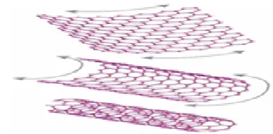
Carbon nanotubes (CNT) are cylindrical structures of carbon (C) atoms arranged in a honeycomb pattern. Figure 28a shows the structure of a single-walled CNT. A CNT can be considered as a graphene layer rolled up to form a seamless cylinder. The diameter of a CNT varies between 1nm and 10nm and lengths up to several mm have been realized. The quasi one-dimensional structures of CNTs yield exceptional electron transport properties (Philip Wong et al., 2011). For instance, CNTs exhibit ballistic carrier transport at room temperature with a mean free path of around 0.7μm and a carrier mobility of 10000cm2/Vs or more (Jacques L. Athow et al., 2011). Besides single-walled CNTs exhibiting a single graphene shell also multi-walled CNTs exist, composed by several nested CNT cylinders (Max Shulaker et al., 2013). CNTs are interesting components for further miniaturization of electrical circuits and have the potential to be used in a
multitude of nanoelectronic, nanoelectric, and nano
[image:10.595.335.528.528.623.2]electromechanical devices, such as sensors and antennas, field-emission sources, energy and data storage elements, nanotube FETs, and many more.
Figure 28. Structure of carbon nanotubes. Left side: single wall. Right side: multi-wall
Due to the chirality, i.e the way the graphene sheet is rolled up, an additional quantization in the circumferential direction is introduced in CNTs. This yields an energy gap that is only dependent on the geometry of the CNT. Therefore, the way the graphene sheet is rolled up results in an energy gap which varies between 0 and 1eV. CNTs with vanishing energy gap are denoted as metallic or zero-gap nanotubes and the others are semiconducting nanotubes. The possibility to adjust the electric transport properties without the need of doping as required in conventional semiconductors makes CNTs so attractive for future electronics. Moreover, CNTs exhibit an extremely high modulus of elasticity and a high thermal conductance (SonalShreya and RajeevanChandel, 2014). Carbon nanotubes have demonstrated an impressive potential during a big selection of application together with field effect transistors and high frequency electronics, chemical sensors, thin film transistors and display electronics. CNT is one among the rising technologies with high potency and a good vary of applications in many alternative streams of science and technology. CNT shows huge promise of less
delay and power consumption than offered Si based
MOSFETs. Power consumption is reduced by replacement CMOS structure by CNT.
Theory of Carbon Nanotubes (CNTs)
Transistor devices for Carbon nanotubes (CNTs) were discovered by Ijima in Japan in 1991. Theoretically, a CNT can be considered as sheet of graphene rolled into a tube (Kunal K Sharma and Reena Monica, 2013). When a honeycomb lattice of a piece of graphene sheet is being rolled into a cylinder, it forms a carbon nanotube, or CNT.
Carbon nanotube can be classified into two main categories:
(i) Single-Walled CNTs (SWCNT).
[image:10.595.39.272.698.766.2](ii)Multi-Walled CNTs (MWCNT).
Figure 29. Rolling of graphene to carbon-nanotube
A.Single-Walled CNTs (SWCNT)
Single-walled carbon nanotubes (SWNTs) are seamless cylinders comprised of a layer of graphene. They have unique electronic properties which can change significantly with the chiral vector, C = (n, m), the parameter that indicates how the graphene sheet is rolled to form a carbon nanotube.
They can be classified as
Armchair
Zigzag and
Chiral vector is a common term used to represent the way grapheme sheet is rolled up to form a nanotube. It is represented by two integer numbers nand m is normally define as (n, m). With this, its circumferential direction can be formulated as:
[image:11.595.48.272.153.260.2]where a1 and a2 are the vectors of the graphene sheet.
[image:11.595.54.275.299.380.2]Figure 30. Lattice structure of different types of CNT
Figure 31. Lattice vectors of a 20 graphene sheet
When m=O, the nanotube are known as zigzag. When n=m, the nanotubes are known as armchair. Else, they are called chiral. Depending on the chiral vector (n, m), a SWNT can be either a semiconductor or metallic material. This property is due to a particular band structure of the graphene sheet and the wrapping in a cylindrical shape that leads to the existence of cyclic boundary conditions. In practical SWNT can possess metallic characteristic if n-m is an integer multiple of 3. If not, it will be asemiconductor (Pranay Kumar Rahi et al., 2015).
The diameter of the nanotube can be expressed as
B.Multiwalled CNT
Multi-walled carbon nanotubes (MWNTs) contains multiple rolled layers of graphene. MWNTs haven't been well-defined because of their structural complexness and selection compared to SWNTs (www.sigmaaldrich.com). Still, MWNTs exhibit benefits over SWNTs, like easy production, low product price per unit, and increased thermal and chemical stability. In general, the electrical and mechanical properties of SWNTs will change once functionalized, because of the structural defects occurred by C=C bond breakages throughout chemical processes. However, intrinsic properties of carbon nanotubes is preserved by the surface modification of MWNTs, wherever the outer wall of MWNTs is exposed to
chemical modifiers (www.sigmaaldrich.com). Double-walled carbon nanotubes (DWNTs) are mix of single-walled and multi-walled nanotubes, showing intermediate properties between the two sorts. DWNTs are comprised of exactly two concentric nanotubes separated by 0.35 – 0.40 nm, with enough band gaps to be used in field-effect transistors. The inner and outer walls of DWNTs have optical and Raman scattering characteristics of every wall.in theory, if every wall behaves like a SWNT (www.sigmaaldrich.com). DWNTs will contains four mixtures supported the electronic type (metallic or semiconducting) in keeping with (n, m) values of their inner and outer walls, e.g., metallic (inner-outer), metallic-semiconducting, semiconducting-metallic, and semiconducting -semiconducting. Some experimental studies found that even if each walls are semiconductive, DWNTs might behave as a metal. This complication of their overall electrical behavior has restricted the utility of DWNTs to applications like thin film electronics. However, DWNTs additionally exhibit many useful properties determined from MWNTs, like improved lifetimes and current densities for field emission and high stability under aggressive chemical, mechanical, and thermal treatments beside the flexibility discovered with SWNTs. Selective functionalization of the outer wall has LED to the employment of DWNTs as core-shell systems manufactured from a pristine carbon nanotubecore and chemically-functionalized nanotube shells, that are applicable as imaging and therapeutic agents in biological systems. DWNTs are often utilised in gas sensors as sensitive materials for the detection of gases like like H2, NH3, NO2 or O2, dielectrics, and technically demanding applications, like field-emission displays and photovoltaic (www.sigmaaldrich.com).
Carbon nanotubes is used for a large range of latest and existing applications (www.sigmaaldrich.com):
Conductive plastics
Structural composite materials
Flat-panel displays
Gas storage
Antifouling paint
Micro- and nano-electronics
Radar-absorbing coating
High useful textiles
Ultra-capacitors
Atomic Force microscope (AFM) tips
Batteries with improved time period
Biosensors for harmful gases
Extra robust and conductive fibresTargeting Drug
Delivery
Bioengineering applications like energy storage and
conversion devices, radiation sources, and hydrogen storage media
Carbon Nanotube Field-Effect Transistor
power consumption. Due to important property that, the CNTs are resistant to temperature changes, meaning they function almost just as well in extreme cold as they do in extreme heat all the above mentioned technologies can be replaced. CNFET Nano electronics can achieve significantly greater performance at a fraction of the switching energy. CNTFET could be a three-terminal device consisting of a semiconducting nanotube delivery two contacts (source and drain), and acting as a carrier channel, that is turned on or off electrically via the third contact (gate). Presently, there are many sorts of CNTFETs are invented, however, CNTFET geometries is also classified in two major categories:
Planar and
Coaxial CNTFET,
[image:12.595.322.542.98.307.2]whether or not planar or coaxial, depends on straightforward principles, whereas being ruled by extra phenomena like 1D density of states (DOS), ballistic transport, and phonon scattering (DurlabhaChaudhary et al., 2013).
Figure 32. Structures of CNTFETs: i) planar gate: a.Bottom or back gate CNFET, b. Top gate CNFET, ii) coaxial gate CNFET.
Planar CNTFETs (Figure 32a) represents the bulk of devices fabricated up to now, largely because of their relative simplicity and moderate compatibility with existing producing technologies. Two structures are possible in planar CNFETs namely
Top gate and
Bottom gate CNFETs.
The coaxial geometry (Figure 32b) maximizes the capacitive coupling between the gate electrode and the nanotube surface, thereby causing additional channel charge at a given bias than alternative geometries. This improved coupling is fascinating in mitigating the short channel effects that plague technologies like CMOS as they drawback device features.
Below Fig shows the arrays of carbon nano tubes for channel functioning
Figure 34 shows a cross section and a top view of a CNFET with an array of three single-wall (SW) CNTs used as a channel (Laxmi N. Pawar et al., 2014). The fabrication of CNFET-based circuits is still in the early stage of development and is facing major challenges such as,
1) Variation in the diameter of tubes,
2) The presence of metallic tubes, and
[image:12.595.52.275.313.446.2]3) Misalignment of Carbon Nanotubes (CNTs) during the fabrication of CNFETs.
Figure 33. Schematic of carbon Nanotube field effect transistor. (a) Internal structure of CNTFET. (b) Top section view
The performance, power and yield of circuits designed with carbon nanotubetransistors arenegatively influenced by these imperfections. In our study, we assume that proper techniques are used to mitigate tube misalignment problem by proper layout designs (Benfdila et al., ?) of CNFET-based gates and CNTs are perfectly aligned in thearray (Laxmi N. Pawar et al., 2014).
Figure 34.(a) Cross section of CNFET (b) Top view of CNFET with an array of f our CNTs
There is a continuous research effort to address fabrication issues in CNFET technology. Various techniques have been proposed to model and simulate CNFETs, and to evaluate their potential performance at the device-level in the presence of metallic tubes. The logical effort technique is used at CNFET device-level, as well as circuit-level, to evaluate the delay in the presence of metallic tubes. In (Kunal K Sharma and Reena Monica, 2013), the logical effort is used to find the minimum delay for a given circuit by changing the number of tubes in the circuit gates, while assuming that only semiconducting tubes are being present (ideal case). In reality, it is very hard to ensure the exact number of tubesbeing present in each CNFET because of fabrication challenges (Laxmi N. Pawar et al., 2014).
Cntfet device description
[image:12.595.319.547.442.516.2]2015). A typical device structure of MOSFET like carbon nanotube FET (CNTFET), which consists of drain, gate, source and substrate, is shown in Fig. 35.
Figure 35. A 2D device structure of CNTFET
Graphene sheets are rolled at certain angle results in carbon nanotube (CNT). Depending on the chirality (i.e., the direction in which the graphene sheet is rolled), a single-walled CNTcan be either metallic or semiconducting. This unique property of the SWCNT is referred to as chirality vector and represented by the integer pair (m, n), called the chiral vectors. The nanotube is metallic if n=m or n-m= 3i, where i, is integer. If this condition is not met then the nanotube is semiconducting. Parallel semiconducting CNTs are grown or transferred to a substrate of CNTFET. The CNT is inserted in the channel region and it is kept undoped, while the other two regions are heavily doped, thus forming the source/drain extended region and/or interconnects between two adjacent devices. The gate voltage then controls the conductivity of these undoped regions. A ballistic or near-ballistic transport can be obtained under low voltage bias with CNTs due to the ultralong (1μm) mean free path (MFP) of CNTs for elastic scattering. A typical structure of a MOSFET like CNTFET device is illustrated in Fig. 35. By positioning additional CNTs, a linear increase in current can be achieved; however, depending on the distance between CNTs (pitch) and the diameter of each CNT, the current cannot be increased linearly with the number of CNTs in a CNTFET because a small pitch causes the so-called screening effect to occur and the diameter determines the amount of current in a CNT. A carbon nanotube is inserted in channel, this is undoped, whereas the other regions are heavily doped, acting as both source/drain. For a MOSFET like CNTFET, behavior of both positive-FET (pFET) and negative-FET (nnegative-FET) are similar. The current density of carbon nanotube (CNT) is very high. Also, CNT has higher carrier velocity with ballistic transport (vF= 8x10
7
cm/s). Ballistic transport is a current transport mechanism in which the very same electron that enters one side of the tube appears at the other side of tube.
Fig.35 shows the potential difference in channel region with ballistic transport. The potential difference, μs-μs’ and μd-μd’ are determined by both the applied bias, here μs and μd are the source and drain Fermi-levels respectively. Solid arrow line in diagram shows the Fermi level profile from source to drain. AMOSFET like CNTFET operates on the principle of barrier height modulation by application of gate potential. The energy bandgap of CNTFET is reciprocally proportional to the diameter of CNT (DCNT) is given as
….. (1)
Where, a= 0.249nm is lattice constant, m and n are integers giving the chiral number a vector of CNT.
The energy bandgap (EG) in eV of CNT is given as (Pranay Kumar Rahi et al., 2015)
………. (2)
For conduction to start, the barrier at source channeljunction has to be overcome energy EG /2 (=Δ1 , say). As barrier height determines the threshold voltage of an FET, the threshold voltage (Vth) in volts of CNTFET is given as
……… (3)
The drain current (ID) in CNT is given as
…………(4)
Where KB, T and h are Boltzmann constant, equilibrium temperature and Plank’s constant respectively.
………….(5)
ξi is a constant for i =s, d, Δ1 half the band gap of CNTFET, ψsis the surface potential and μi is Fermi level.
There are three current sources in CNTFET model
(i) Thermionic current contribution by semiconducting
subbands,
(ii) The current contribution by metallic subband, and
(iii) Leakage current caused by band to band tunnelling mechanism
The DC characteristics of n-type CNTFET simulated using HSPICE using CNT model (Mike Sereda, 2016; Manisha, Archana, ?) are shown in Fig.36. From Fig. 36 it can be depicted that the DC characteristic of n-type CNTFET has a very similar trend like that of an nMOS. CNTFET exhibits unipolar behavior by suppressing either electron (pFET) or hole (nFET) transport with heavily doped source/drain. The gate-source biasing modulates the non-tunnelling potential barrier in the channel region, and thereby the conductivity. Better gate electrostatics can be achieved by using high-k, e.g. HfO2, gate dielectric material (Benfdila et al., ?). The CNTFET circuit performance changes with the diameter of CNT. With varying chiral number (m, n) of thetube drain current varies, which is shown in Fig. 37. Supply voltage is 0.9V. It is also seen that with decreasing diameter drain current reduces drastically.
Properties of Carbon nanotubes as follows (Pramod Yeole and Dinesh V. Padole, 2015)
Excellent electrical properties: Ballistic transport in
metallic tubes, highest carrier mobility in
semiconductor tubes.
Thermal: highest thermal conductivity.
Trans-conductance: Device has large trans conductance, which indicates a great potential for Nano electronic circuits (Chris Dwyer et al., 2004).
Mechanical properties: Highest young's modulus,
highest tensile strength.
Depending on the chirality and diameter of carbon nano
tubes, it can be used as eiher metals or semiconductors (JieDeng et al., 2007).
Effect of temperature on threshold voltage is negligibly
small.
It has capability of setting desired threshold voltage by adopting proper diameters for nano tubes. This characteristic of CNFET is suitable for designing high performance multiple threshold voltage structure and have very high driving capability.
[image:14.595.42.288.53.480.2]
Figure 36. DC characteristics of n-type CNTFET
Figure 37. DC characteristics of n-type CNTFET with variable chirality of nanotube for a supply voltage of 0.9V
The high performance carbon Nanotube Field Effect transistor (CNTFET) is used along with Gate Diffusion input (GDI) technique to design low power, area efficient and high performance logic circuits maintaining less complexity (PramodYeole and Dinesh V. Padole, 2015). Different logic styles were described to reduce power and delay which will be helpful for researchers to replace CMOS technology by
CNFET (Manoj Kumar et al., 2012). Today's CNT process
improvements are insufficient to overcome challenges of imperfections and variations essential to CNTs; design and processing techniques, together with a probabilistic analysis framework, for robust CNFET digital VLSI circuits immune to inherent CNT imperfections and variations. To overcome the challenges of the CNFET technology by retaining its energy-efficiency benefits, there are considerable improvements in design tools which enable robust and scalable CNFET circuits.
As per survey the simulation of digital circuit using CNFET are as follows
Simulations are done by using HSPICE model of
CNTFET (Durlabha Chaudhary et al., 2013). The
fabrication feasibility is high in CNTFET than MOSFET and CNTFET having superior device
performance than MOSFET (Durlabha Chaudhary et
al., 2013).
Synopsys HSPICE with 32nm CNFET technology is
used to simulate the ternary Full Adders to evaluate their performance and to confirm the correct operation in the survey (Pranay Kumar Rahi et al., 2015).
Due to superior transport properties, excellent thermal conductivities and high current handling capacities of Carbon nanotubes have proved to be a potential heir to Si (Benfdila et al., ?).
CNFET-based digital arithmetic and storage circuit are fabricated using conventional optical lithography steppers and fabrication tools, some of them at full wafer scale. CNT interconnects with sub-ns delays have been measured using ring oscillators in survey (Benfdila et al., ?).
An improvement of power delay product was increased
by factor 17 times with CNT (Kunal K Sharma and Reena Monica, 2013).
A complete sensor interface were implemented entirely
using CNFETs that can be fabricated reproducibly in a
VLSI-compatible fashion, which successfully
overcomes major obstacles for CNFET-based circuits: mis-positioned and metallic carbon nanotubes (CNTs).
Performance of CNFET based digital circuits were
analyzed by decreasing the diameter of CNFET & it is found that power reduces with delay penalty.
CNFET based power efficient digital event count
comparator were designed and simulated using Cadence Virtuoso, the result shows that the design consumes significantly lower power and has lower delay (Mehdi Masoudi et al., 2014).
The ternary Full Adders are simulated using Synopsys
HSPICE (Mohammad Hossein Moaiyeri et al., 2012).
Performance of CNFET based digital circuits were
analyzed by decrease in diameter of CNFET & it is found that power reduces with delay penalty. The circuits have been simulated using HSPICE (Sonal Shreya and Rajeevan Chandel, 2014).
CNFET based power efficient digital event count
comparator were designed and simulated using Cadence Virtuoso, the result shows that the design consumes significantly lower power and has lower delay (Ronak
et al., 2014).
Application of CNFET
Using CNFET, digital circuits can be constructed such as full adders, multiplexers (Mehdi Masoudi et al., 2014), counters (Kunal K Sharma and Reena Monica, 2013).
Digital signal processing (DSP), image processing and performing arithmetic operations in microprocessors (Pranay Kumar Rahi et al., 2015).
Adder circuit design (Manoj Kumar et al., 2011) and multiplier circuits.
Through a set of custom-design automated scripts,