UART Controller : Design Synthesis and Power
Optimization
Priya Singh1, Mukul Anand2 1
Senior Design Engineer, Synapse Techno Design Innovations Private Limited 2
Technical Team Lead, EInfochips Ltd. (An Arrow Company)
Abstract: Universal asynchronous receiver transmitter, abbreviated UART is an integrated circuit that serves as a serial communication protocol; mostly used for short-distance, low speed, low-cost data exchange between computer and peripheral. The UART takes bytes of data and transmits the individual bits in a sequential fashion. At the destination, a second UART re-assembles the bits into complete bytes. So a UART includes both receiver and transmitter module .This paper presents hardware implementation of UART both functional and synthesizable and optimized in terms of power via Clock Gating. The design is implemented in Verilog HDL and simulated using both Modelsim and NCSim, simulators. The code has been verified for following the synthesizability rules using Atrenta Spyglass and synthesis is carried out using Synopsys design compiler, later the concept of Clock Gating has been applied to turn of the FSM of both transmitter and receiver module when no transmission or reception occurs. For the purpose of using this UART on any SoC, interfacing has been carried out using skyblue line interface. With the help of interfacing there is no need to change the number of input or output pins if some more functionalities need to be incorporated, as per the SoC needs.
Keywords: System on chip (SoC), Universal Asynchronous Receiver and Transmitter (UART),Clock Gating (CG), UART control register (UARTCR), UART status register (UARTSR).
I. INTRODUCTION
Asynchronous serial communication has advantages of less transmission line, high reliability, and long transmission distance; therefore it is widely used in data exchange between computer and peripherals [1]. Universal asynchronous receiver/transmitter is basically used between the peripheral devices. For example: computer and printer or in between the controller and mouse. Hence UART is used mostly for the short distance, low speed and is thus of low cost.
This paper uses the Verilog hardware description language to implement the core functions of UART, as a transmitter and a receiver using the FSM methodology and then synthesizes the hardware using Synopsys design compiler tool. As we are using the state machines for transmitter and receiver our design become less complex and the proposed UART consumes lesser area.
For integrating the synthesized UART on to the SoC, we interface the UART designed via skyblue line signals. Skyblue line is a Motorola‘s standard bus widely used in industry.
Next the concept of State Machine controlled global Clock Gating [2] has been applied to reduce the unnecessary power consumptions in the design. And the results proves the essence of this technique.
II. PROPOSED DESIGN OF UART
Fig1 shows the top view of UART; this UART is governed by a clock signal ipg_clk and a reset signal. inputs Here tx is the output pin to carry out any kind of serial transmission and rx serves as the input pin which receives the serial data bits wrapped with start, stop and parity bit.
,ips_byte_31_24.
A. Setting up Internal Registers
We will be using two registers used for designing the transmitter and receiver module [3], there complete details and description is as written next.
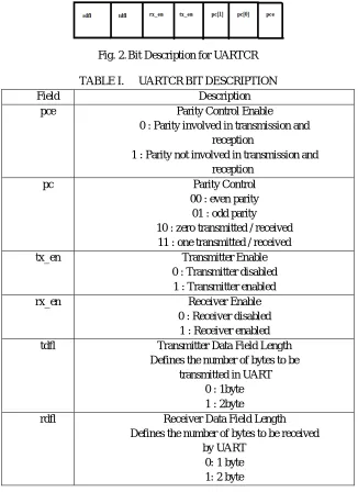
[image:2.612.144.470.238.686.2]1) Control Register: This register contains necessary settings for the UART. And it must be set prior to use. Some common settings include: Number of data bits, number of stop bits, parity control, UART TX/RX enable/disable etc. In our designed UART following are the control bits we have considered and accordingly worked upon, as shown in fig 2 and the complete bit description is shown in table I.
Fig. 2.Bit Description for UARTCR
TABLE I. UARTCRBITDESCRIPTION
Field Description
pce Parity Control Enable
0 : Parity involved in transmission and reception
1 : Parity not involved in transmission and reception
pc Parity Control
00 : even parity 01 : odd parity 10 : zero transmitted / received
11 : one transmitted / received
tx_en Transmitter Enable
0 : Transmitter disabled 1 : Transmitter enabled
rx_en Receiver Enable
0 : Receiver disabled 1 : Receiver enabled
tdfl Transmitter Data Field Length
Defines the number of bytes to be transmitted in UART
0 : 1byte 1 : 2byte
rdfl Receiver Data Field Length
Defines the number of bytes to be received by UART
0: 1 byte 1: 2 byte
Fig. 3.Bit Description for UARTSR
TABLE II. UARTSRBITDESCRIPTION
Field Description
Pe Parity Error flag, indicates if
There is any Parity Error in the Corresponding byte.
0: No parity error 1: Parity error
Dtf Data Transmission Complete Flag, set
indicates data Trans -mission is complete.
Drf Data Reception Flag a set indicates
data received.
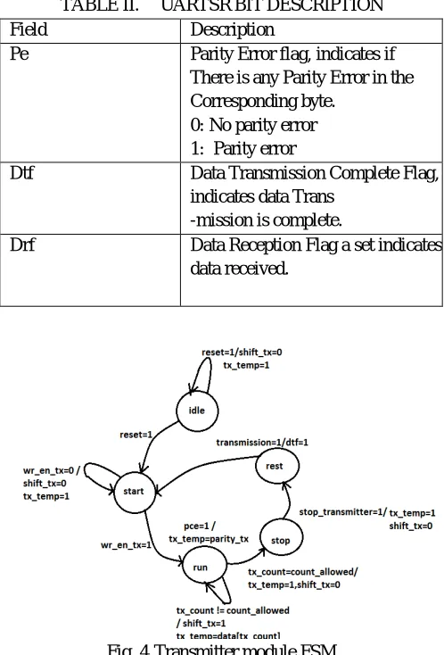
B. UART Data Transmission
Fig. 4.Transmitter module FSM
As per the FSM designed [4], transmission begins with the bit ‘1’ followed by a start bit‘0’; when the tx_en signal is high (transmission is enabled) this is then followed by 8/16-bit data, depending on the length of data field to be transmited (tdfl) next a parity bit will be sent if pce is set and at last a stop bit ‘1’. The start signal here indicates to the receiver that transmission of data is about to start. Parity bit is meant for error detection. Stop bit indicates the end of transmission to the receiver. Each character is placed in between start and stop bits, this is called framing. The start bit is always low and stop bit is always high The LSB of the data word is transmitted first.
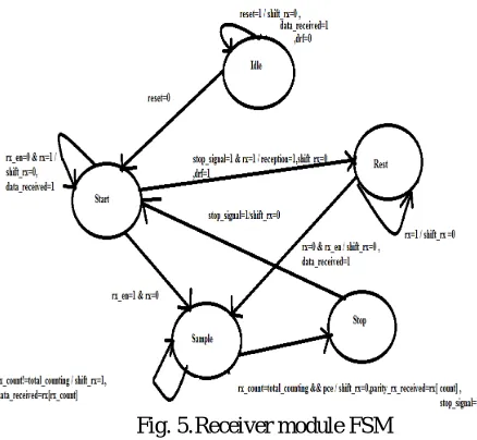
C. UART Data Reception
[image:3.612.182.431.156.523.2]Fig. 5.Receiver module FSM
III. POWER OPTIMIZATION STRATEGY
The UART serial protocol lends itself well to state-machine-controlled global clock gating.
1) Transmitter FSM Clock Gating: The transmitter FSM should turn on only when there is some data coming at the data register for the purpose of transmission. In case there’s no info to be transmitted the clock is made to stop from reaching the Transmitter module of the UART thereby avoiding a lot of power wastage that occurs due to the switching activities continuously.
2) Receiver FSM Clock Gating: When the serial receive input rx is idle (high) in between transmissions, there is no need to provide a clock to the majority of flip-flops in the deserializer circuit i.e receiver module of this UART. The only flip-flop that requires an uninterrupted clock is the receive detection flip-flop that constantly sense the receive input for an incoming transmission that is the rx pin of the UART controller. The state machine for the proposed receiver is designed to cut off the clock signal to most flip-flops during the Idle state. When incoming data is detected (rx pin goes 0, start bit is detected), the state machine restarts the internal clock to process the received data. This technique inherently reduces power consumption during idle periods.
IV. SIMULATION RESULTS
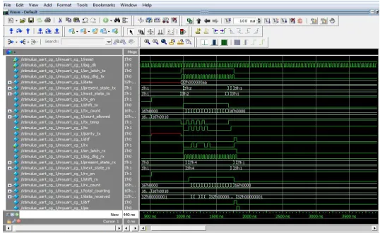
[image:4.612.131.481.505.715.2]The Simulation results of the transmitter and receivers module on a Modelsim and NCSim simulator is as shown below in fig.6 and fig.7 , Transmitters simulation results are done on Modelsim 10.3 simulator and the receivers is done on cadence NCSim simulator , functionality is properly met.
Fig. 7.Simulation Result-Receiver
V. SYNTHESIS RESULTS
The final synthesis is carried out on Synopsys Design Compiler results in the following hardware generation. This synthesis has been carried out on a 45 nm technology.
[image:5.612.179.433.324.454.2]The hardware implementation has been carried out for this UART design when it is simultaneously doing transmission and reception of data meaning a full duplex operation is being performed.
Fig. 8.Synthesis Result–UART carrying out a full duplex operation
VI. CLOCK GATING RESULTS
The State Machine controlled global Clock Gating concept when implemented by making changed in the HDL of this UART code results in the functionality being met similar to the previous case , as shown in fig.9; but with an overall power reduction. To compute the power loss in case with and without Clock Gating we use Xilinx Power Estimator 11.1 tool and the results are as shown next in table III.
[image:5.612.178.447.549.714.2]UART (no CG)
10 ns 1 ns 0.1ns 10 ps 1 ps
0.010 0.039 0.329 3.233 32.268 0.171 0.200 0.492 3.414 32.523 UART (with CG)
10 ns 1 ns 0.1ns 10 ps 1 ps
0.010 0.038 0.163 3.204 31.978 0.171 0.200 0.489 3.384 32.232
VII. CONCLUSION
This UART uses Verilog as the design language to achieve the receiver and transmitter modules. Finally for the usage of this UART on to any processor or SoC in future we have provided skyblue line interface. With the help of this interfacing, if we wish to incorporate few more characteristics in the design we can do so without impacting on the number of input or output pins of the top module. Functionality has been properly verified using Modelsim and NCSim simulators and the synthesis has been carried out on a 45 nm technology using synopsys design compiler. The circuit has even been optimized in terms of Power through the concept of Clock Gating, which turns off the FSM of transmitter and receiver when no transmission or reception operation is to be carried out.
VIII. ACKNOWLEDGMENT
First and foremost I would like to express my deepest gratitude to Mr. Rivu Das, Technical Lead at eInfochips Ltd. (An Arrow Company) and Mukul Anand, Technical Lead, at eInfochips Ltd. (An Arrow Company) for his invaluable support, guidance, motivation and encouragement throughout the period this work was carried out. .
REFERENCES
[1] B.Jeevan & M.Neeraja, “DESIGN AND SIMULATION OF UART PROTOCOL BASED ON VERI VERILOG,” International Conference on Electronics and Communication Engineering (ICECE) -16th Sept, 2012.
[2] Casey T. Morrison, William Goh, Saeed Sadrameli, and Eric Blattler, “Design and Evaluation of a Low-Power UART-Protocol Deserializer”.
[3] IP Interface, Semiconductor Reuse Standard, SRS V3.1, MOTOROLA, 01 NOV 2002.
[4] Clifford E. Cummings, “State Machine Coding Styles for Synthesis,” Sunburst Design, Inc. SNUG 1998.