.
-
'.,
INCOTERM Corporation
FIELD ENGINEERING T EC HNI CAL MANUAL
SPD™ 10/20
STORED PROGRAM DISPLAY
SPDTM
"This document contains information proprietary to INCOTERM Corporation and is delivered on the express condition that it is not to be dis-closed, reproduced in whole or in part, or used for manufacture for anyone other than INCOTERM Corporation without its written consent, and that no right is granted to disclose or so use any in-formation obtained in said document. This re-striction does not limit the right to use information obtained from another source. 11
TABLE OF CONTENTS
Chapter
LIST OF ILLUSTRATIONS LIST OF TABLES
ix xi I II III IV INTRODUCTION 1. 1 Scope
· 1-1 1-1
1. 2 General Specifications 1-1
1. 3 Configuration 1 -1
1. 3. 1 Minimum Configurations 1-2
1. 3. 2 Units Available for Expanded Configurations 1-2
1. 4 Reference Documents 1-3
INSTALL.A TION
2. 1 Visual Inspection 2. 2 Configuration Chart 2. 3 Site Preparation 2. 4 Installation
2. 4. 1 Cabling of Product 005, Model 00010 2. 4. 2
2. 4. 3 OPERATION
Cabling of Product 005, Model 00011 Cabling of Product 005, Model 00014
3. 1 General Information 3. 2 Keyboard
3. 2. 1 Introduction
2-1 2-1 2-3 2-10 2-10 2-10 2-13 2-13 3-1 3-1 3-1 3-1
3. 2. 2 Key Functions 3-2
3. 2. 3 Indicator Functions 3-6
3. 3 Initial Turn On and Check Out 3 -6
3. 3. 1 Initial Turn On Procedures and Indications 3-6 3. 3. 2 Programmed Operation
SYSTEM DESCRIPTION 4. 1 Introduction
4. 2 System Functional Description
Chapter
V
TABLE OF CONTENTS (Cont. )
4. 2. 1 4. 2. 2 4. 2. 3
General Information
Terminal Processing Unit Interface Control
4. 3 Addressing and Instruction Formats 4. 3. 1 Introduction
4. 3. 2 4. 3. 3 4. 3. 4 4. 3. 5 4. 3. 6
Hexadecimal Notation Word Formats
Instruction Classes
Effective Address Calculation
Basic System Timing and Data Flow THEORY OF OPERATION
5. 1
5. 2
Logic Utilized
5. 1. 1 Logic Levels
5. 1. 2 Schematic Interpretation Data Flow Electronics
5. 2. 1 Introduction
5. 2. 2 General Discussion of Data Flow 5. 2. 3 Bus System
5. 2. 4 Memory Address Register 5. 2. 5 Arithmetic Unit Adder 5. 2. 6 Arithmetic Unit Bus
5. 2. 7 Auxiliary Arithmetic Unit 5. 2. 8 Character Register
5. 2. 9 Line Register
5. 2. 10 Accumulator Register 5. 2. 11 Condition Store Register 5. 2. 12 Program Counter Register 5. 2. 13 Test Com para tor
5. 2. 14 Bus Enable Decoders for the MDR 5. 2. 15 Memory Data Register
5. 2. 16 Memory Data Bus Drivers
Chapter
TABLE OF CONTENTS (Cont.)
5. 2. 17 Exclusive-Or Unit
5. 2. 18 TPU Register-Clock Drivers 5. 3 Data Control Electronics
5. 3. 1 5. 3. 2
5. 3. 3
5. 3. 4 5. 3. 5 5. 3. 65. 3. 7
5. 3. 8 5. 3. 9General Information
Instruction Register and Decoder Generic Opcode Decoder
Miscellaneous Control Functions State Counter
Auxiliary Arithmetic Unit Arithmetic Unit Control Real Time Clock Module Interrupt Controls
5-20 5-21 5-21 5-21 5-25 5-26 5-27 5-35 5-39 5-43 5-45 5-46 5. 3. 10 Controller Decoder and Wired Option Matrix 5-48
5. 3. 11 Control Line Drivers 5-49
5. 4 Memory Electronics 5-49
5. 4. 1 Introduction 5-49
5. 5
5. 4. 2
5. 4. 3 5. 4. 4 5. 4. 5 5. 4. 6
General Discussion of Memory Organization and Operation
X and Y Drivers and Associated Logic Inhibit Logic and Drivers
Memory Stack Sense Electronics Memory Sense Logic
Timing and Refresh Electronics 5. 5. 1
5. 5. 2 5. 5. 3 5. 5. 4 5. 5. 5 5. 5. 6 5. 5. 7 5. 5. 8
Introduction
20-Phase Clock Timing Unit
Control, Start and Last Line Control Line Computation Logic
Character Code Translator Refresh Video Circuit
Read-Only-Memory and Input Logic ROM Data Buffer
5. 6 High Efficiency Power Supply 5. 6. 1 Operation
Chapter
VI
5. 7
TABLE OF CONTENTS (Cont.)
5. 6. 2 5. 6. 3 5. 6. 4
Operation Regulation Typical Checks Line Lock Oscillator
INPUT /OUTPUT INTERFACE CONTROL 6. 1 Input/ Output System
6. 2 Keyboard
6.
36. 4
Keyboard Controller 6. 3. 1 Introduction 6. 3. 2 Input/Output Data 6. 3. 3 Control Logic Asynchronous Controller 6. 4. 1 General
6. 4.
26.
4. 36.
4.4
6.
4.5
6.
4.6
Timing Circuits
Input/ Output Commands Write Mode
Read Mode Boot Mode 6. 5 Synchronous Controller
6. 6
6. 7
6. 5. 1 General 6. 5. 2
6. 5. 3
Circuit Options
TPU Control and Modem Interface 6. 5. 4 Multiplexer Operation with Synchronous
Controller
6. 5. 5 Synchronous Operation in BOOT Mode 6. 5. 6 Basic Operation
Split Screen Controller 6. 6. 1 Operation Boot Controller
6. 7. 1
6. 7. 2
6. 7. 3Introduction
Remote Load Sequence Boot Controller Circuitry
Chapter VII
7. 1 7. 2 7. 3
7. 4 7. 5 7. 6
TABLE OF CONTENTS (Cont.)
General
Field Substitution Test Console 7. 3. 1
7. 3. 2
Wiring Procedure
Detailed Explanation of Control Switches Test Points Not Console Tested
Waveforms
CRT Adjustments
APPENDIX A-SIGNAL MNEMONICS APPENDIX B-OPTION BLOCKS
APPENDIX C-MISCELLANEOUS CABLE DATA
Figure
1-1
1-2
2-1
2-2
2-3 2-4 2-52-6
2-7
2-8
2-9
3-1 4-1 4-2 4-3 4-4 4-5 5-1 5-2 5-3 5-4 5-55-6
5-7 5-8 5-95-10
5-11LIST OF ILLUSTRATIONS
Minimum Terminal Configurations SPD Product Line
Factory Packing
Removal of Plywood Base
Circuit Board Identification and Location
Bottom View of Terminal Showing Fuse and Connector Locations
TPU Chas sis Photo
Actual Bottom View Photo Sample Shipping Memo
Cabling Diagram Dual Display Cabling Diagram Master Terminal Typical Keyboard Arrangement
SPD 10/20 Stored Program Display System Circuit Board Identification
2K Core Memory Layout Effective Address Calculation System Timing Example
Integrated Circuit Pin Identification
Simplified Block Diagram TPU Data Flow Data Flow Module
Data Control Circuit Module
Simplified Block Diagram Data Control
Detailed Block Diagram Instruction Register and Decoder
Memory Electronics Module Memory Module
Simplified Block Diagram Memory System Simplified Functional Diagram and Logic Table SN 7 5324 Memory Driver
Memory Timing
Figure 5-12 5-13 5-14 5-15 5-16 6-1 6-2 6-3 6-4 6-5 6-6 6-7
6-8
6-9 6-106-11
7 -1 7-2 7-3 7-4 7-5 7-6 7-7LIST OF ILLUSTRATIONS (Cont. )
Refresh Module Timing Unit
Simplified Block Diagram Refresh Module Refresh Module Timing Unit
Internal View Power Supply
Simplified Block Diagram Power Supply Line Lock Oscillator Schematic
Code Chart, 1090-C Keyboard
Simplified Keyboard Block Diagram Current Path Illustrated for J Key
Keyboard Controller
Typical Keyboard Lamp Driver Circuit Asynchronous Controller
Block Diagram Asynchronous Controller Synchronous Controller
Split Screen Controller
Simplified Block Diagram Split Screen Controller Split Screen Timing
Simplified Diagram Boot Controller
Bottom View of Terminal Illustrating Voltage Test Points and Adjustment Locations
Keyboard Bottom View INCOTERM Test Console
Controller Circuit Board Extender Computer Circuit Board Extender T. V. Monitor Adjustments
Cathode Ray Tube Adjustments
Table 1-1 1-2 2-1 4-1
4-2
5-1
6-1
6-2
7-1 7-2 7-3LIST OF TABLES
SPD 10/20 TPU Specifications
SPD Product Physical and Electrical Data Configuration Chart
SPD 10 / 20 Controllers, Related Function and External Devices
Decimal, Binary and Hexadecimal Equivalents Integrated Circuit Reference Table
Keyboard Connectors
Asynchronous Controller Option Blocks Field Problem Identification
Test Point Wiring From TPU to Console Test Points Not Console Tested
Page 1-3 1-4 2-8
4-7 4-8 5-3
6-4
6-15
FOREWORD
I> ,r G .u - r ' ,~ ""
1. 1 SCOPE
CHAPTER I INTRODUCTION
The purpose of this manual is to provide Field Engineers with pre-liminary data concerning the SPD 10/20 Stored Program Display Terminal.
Two levels of information are required within the Field Service organization. First, the Field Repair philosophy dictates repair by replacement of assem-blies and subassemassem-blies; and, secondly, Depot repair requires replacement of components in assemblies and subassemblies returned from the field. This manual is organized to fulfill both levels of maintenance.
1. 2 GENERAL SPECIFICATIONS
The SPD 10/20 is a CRT display containing a stored-program com-puter. The built in computer allows the terminal to be programmed and optimized for any specific application. It also allows the terminal to operate in any network, with or without a central computer. Table 1-1 contains the operating specifications for the SPD 10/ 20 Display Terminal. Table 1-2 provides both physical and electrical data for the Display Terminal and associated products.
1. 3 CONFIGURATION
item. The terminal computing circuitry, Display CRT, input output wiring, and housing are included in the baseline configuration. When a customer's order is placed, any required additional hardware is easily included. Con-figuration deviations are caused by each customer's definition of the type of data environment the Terminal will be exposed to. At this point, modular I/0 interface circuitry is added with little or no change necessary to the manufactured terminal.
1. 3. 1 Minimum Configurations
Minimum unit configuration relative to the SPD 10/20 product line is comprised of three terminal utilizations, illustrated in Figure 1-1. First, the basic terminal contains the terminal processor (computer), display, key-board and half duplex communications interface. The second adds a remote display and keyboard manufactured as an auxiliary unit to the basic terminal. The auxiliary is identical in appearance to the basic unit, but does not have a computer or I/0 circuitry. The basic terminal, in this case, becomes a master; the auxiliary is a slave that shares the basic terminal computer. The third is a further extension of the second, which results in two additional input and display stations operating as slaves to the master terminal.
1. 3. 2 Units Available for Expanded Configurations
As an enhancement to the versatility of the SPD 10/20 Display Terminal, INCOTERM has developed a complete family of SPD products. The following paragraphs briefly describe each product. Figure 1-2 illustrates the present SPD product line.
SPd~ Program Loader
Table 1-1. SPD 10/20 Terminal Processing Unit (TPU) Specifications
Type:
Addressing:
Data Word Length: Memory Word Length: Arithmetic Code: Internal Memory:
Memory Cycle: Machine Speed:
Standard I/ 0 Lines:
Parallel binary, byte oriented
Single address with indirect addressing 8-bit byte, 12-bit special word
16 bits, 2 bytes Two's complement
Magnetic core with 2048 16-bit words 1. 6 microseconds
Add: 3. 2 microseconds Subtract: 3. 2 microseconds
8-bit input bus 8-bit output bus 10-bit control bus
8 interrupt lines
SPD TM -M Terminal Multiplexer Unit
The SPD-M provides the capability of interfacing a maximum of 16 terminals to a single modem. When in use, the Multiplexer monitors the communications line and provides ordered transmissions. The Multiplexer can also be cascaded to provide additional terminals with data.
SPD TM -P Printer
The SPD-P is a hard copy output device which prints out messages sent to it by SPD 10/ 20 Terminals. The Printer contains its own multiplexer and can interface with up to 16 SPD 10/20 Terminals. The hard copy form is edge sprocketed measuring up to 14- 7 / 8 inches in width and 11 inches in length. The forms can provide multiple copies. Data input to the Printer conforms to the American Standard Code for Information Interchange (ASCII).
1. 4 REFERENCE DOCUMENTS
[image:17.612.81.538.74.414.2]... I
Table 1-2. SPD Product Physical and Electrical Data ~
Size in Weight Maximum Cable
Inches in Length Power
Unit Type (HxWxD) Lbs. in Feet in Watts Voltage & Frequency
SPD 10/20 18xl8. 5xl9 48 50 - Modem 180 117V+lO%, 60+1 Hz
-300 - Multiplexer1000 - Multiplexer (OPTIONAL)
KEYBOARD 3. 2xl 9x8. 1 7 10 - SPD 10/20 POWERED FROM SPD 10/20 PRINTER 12x3lx26 90 300 - SPD 10/20 450 11 0 to 1 2 5 V, 6 0 ±0, 5 Hz
(Desk) 1000 - SPD 10/20
36x3lx26 (OPTIONAL)
(Pedestal)
MULTIPLEXER 30 50 - Modem ll 7V.±l 0%, 60:±. 1 Hz
9,5xl7xl4 300 - SPD 10/20 120
1000 - SPD 10/20 (OPTIONAL)
PROGRAM LOADER 5xl2x7 10 10 - SPD 10/20 POWERED FROM SPD 10/20 AUXILIARY 18xl8-l/2xl9 40 10 - SPD 10/20 60 117V _±10%, 6o+ 1 Hz
Master Station
Master Station
Master Station
[image:19.612.56.547.47.677.2]SPD-P Printer SPD-M Multiplexer
SPD-10/20 Stored Program Display
SPD-T Tape Cassette SPD -L Program Loader
[image:20.612.40.580.42.702.2]\.
2. 1 VISUAL INSPECTION
CHAPTER II INSTALLATION
Prior to unpacking, check the shipping container for signs of damage in shipment such as crushed or torn areas. Packing at the factory consists of placing the Terminal on a plywood base which prevents lateral movement during shipment. The Terminal is then placed in a cardboard container which serves as an inner container. The inner container is restricted from moving within the outer container by edgemounted shock absorbers. See Figure 2-1
for packaging layout.
As illustrated in Figure 2-1, the Keyboard and associated cables are packed in a separate smaller container. Shipping weight of the Terminal is approximately 60 pounds. Shipping weight of the Keyboard and cables is ap-proximately 10 pounds.
In the event that damage in shipment has occurred or the items re-ceived are not those listed on the Equipment Summary, promptly contact:
James Mahoney IN COT ERM Corp. Phone: 617-481-2000
pins, loose or bent hardware, etc. Remove the plywood base and outer
housing from the Terminal to facilitate visual inspection of the bottom and
inside of the Terminal.
2-2. )
Inner Container
QJ
Inner Sheets (2)
Liner
Plywood Base
Toro-Pads (8)
Outer Container
Figure 2-1. Factory Packing
Cables I
Keyboard
Removal of the outer housing is accomplished as follows. (See figure
(a) Place Monitor protective pad on table and rest Terminal
face down on the pad.
(b) Remove plywood base by removing four retaining bolts.
[image:24.612.57.548.159.589.2]Table
Base
,-
1
~~:::::::==~
I
I
...
,
I
I
I
I
I
Figure 2-2. Removal of Plywood Base
Screws
Retaining Bolts For Shipping Base
(d) Return the Terminal to its proper position and lift outer housing up and away from Terminal.
While the top cover is off, check the circuit boards to see if they are
properly aligned and plugged in, as vibration in shipment could cause board
loosening. See Figure 2-3 for circuit board identification and location.
Check the connectors and fuses that are accessible from the bottom of the
Terminal. See Figure 2-4 for identification and location. Replace top cover
by reversing the removal procedure. Figure 2-5 and 2-6 provide actual
views relating to construction and location of the TPU and associated
com-ponents.
2. 2 CONFIGURATION CHART
Table 2-1, along with the visual inspection and shipping memo
(Fig-ure 2-7), provide a check list to verify that for the given product, model and
serial number, the required boards have been supplied. This table will be
Slot ID No. Board Name
1. Keyboard Controller 9. SPARE (no connector) Half Duplex
2. Communications Controller 10. Memory Electronics
3.
*
11. Memory Stack4.
*
12. CPU Data Flow5.
*
13. CPU ControlRefresh Memory and
6.
*
14. Timing Unit7.
*
A Power Supply 'A' Board8.
*
B Power Supply 'B' Board*
Space for Additional Controller Options or FeaturesD
/
Oscillator
Power Supply
[image:26.612.51.556.59.665.2]POWER SUPPLY TERMINAL
FUSE VALUE VOLTAGE FUSE VALUE VOLTAGE
Fl 2.SA 117Vac Fl 3A 117Vac
F4 1.SA +25Vdc
FS 3A +14Vdc
F6 10A + SVdc F7 3/8A - SVdc F8 3/8A -14Vdc
I/0 Bus Direct Access*
Communications Tenninal
Tenninal
F5
Power Supply 115
F7 Fl
0 0
*
Will commonly be used for Program Loading.Figure 2-4. Bottom View of Terminal Showing Connector Panel and Fus es
Keyboard
d.c. Distribution
[image:27.612.70.555.66.651.2]OSCILLATOR INTERLOCK
•
B2114-23
ERROR ALARM POWER SUPPLY ON OFF
[image:28.612.42.570.106.635.2]BOOT BUTTON 1/0 CONNECTOR PANEL
e
'•
000)2
•
B2102-7 DC VOLTAGE ADJUST
N
I Table 2-1. Configuration Chart
(X)
Board Circuit Board Allocation per Product and Model Number
Slot 005/00010 006/ 00011 005/00012 006/00013 005/00014
1. Keyboard Keyboard Keyboard Keyboard Keyboard
001-03-03 001-03-03 001-03-03 001-03-03 001-03-03
2. Sync Sync Sync
001-08-03 001-08-03 001-08-03
3. Keyboard Keyboard
001-03-03 001-03-03
4.
5. 6.
7.
Split Screen Split Screen Jumper Jumper Jumper001-15-03 001-15-03
8.
9.
NO CONNECTION1
o.
Memory Elec. Memory Elec. Memory Elec. Memory Elec. Memory Elec.001-06-03 006-06-03 001-06-03 006-06-03 001-06-03
11. Memory Memory Memory Memory Memory
Stack 2K Stack 2K Stack 2K Stack 2K Stack 2K
12. TPU Data TPU Data TPU Data TPU Data TPU Data
Flow Flow Flow Flow Flow
N
I
Board Slot
13.
14.
With AUX
Without
AUX
005/00010
TPU Control 005-07-03
Refresh Module and Timing Unit 005-14-03
X
Table 2-1. Configuration Chart ( Cont)
Circuit Board Allocation per Product and Model Number
006/ 00011 005/00012 006/00013
TPU Control TPU Control TPU Control
005-07-03 005-07-03 005-07-03
Refresh Refresh Refresh
Module and Module and Module and
Timing Unit Timing Unit Timing Unit
005-14-03 005-14-03 005-14-03
X
X X
NOTE
Board etch number is listed in Table 2-1 be-cause there is a difference between Product
005 and 006 art work. The Table makes the
different boards clear. Also be aware that the number etched on a given board relates to the artwork and is not a circuit board part
number. The part number is provided on the
Equipment Summary.
005/00014
TPU Control 005-07-03
Refresh Module and Timing Unit 005-14-03
(Custom)
Figure 2-7 is an example of the Shipping Memo which is packed with each system. As stated previously, this data is available at installation time. The data identifies the particular Terminal and should be retained for future reference.
2. 3 SITE PREPARATION
Site preparation is not a critical factor with the SPD 10/20 Terminal. Verify that the site contains a 115 VAC, 60 Hz, 3 wire (hot, common and ground) connector and a cable for connecting the Terminal to the selected communications device, such as a modem. This cable is supplied by INCOTERM at the customer's request.
2. 4 INSTALLATION
On-site installation of the SPD 10/ 20 Terminal requires connecting the cables to the rear of the Terminal, and to external equipment. As in-dicated in Table 2 -1, these instructions are directed toward initial Product Installation.
2.4.1 Cabling of Product 005, Model 00010
The SPD 10/20 Terminal, Model 00010 configuration consists of a Master Terminal and an Auxiliary Terminal. Each Terminal has a Keyboard
Controller, Video Display and Keyboard input unit; however, both Terminals share a single Processor that is contained in the Master unit. Figure 2-8 is a cabling diagram for the Model 00010.
The following instructions define the cable connections required to in-stall an SPD 10/20 Terminal in the Product 005, Model 00010 configuration. Throughout the entire cabling procedure observe proper cable dressing for professional final appearance. Secure each cable with connector hood secur-ing screws. Proceed as follows to install the cabling.
(a) Position the INCOTERM equipment on the desk or table designated by the customer.
.
/-/7-
--
.J
/NCOTERNI
~
~
CORPORAr/ON IHAYES MEMORIAL OAIVE. MARLBOROUGH, MASS. 01752 617-481-2000 TELE>< 94-8.:::a02
SHIP TO • . ' · ·, ·
FRIENDSHI~ ~PORT .
Bal tim~r
G~landHold o
~'lk-up
by Jack Colburn
C-:,
Incoterm Corporation
PURCHASE ORDER NO.
I
SALES ORDER NO. DATEDDATE OF SHIPPER !SHIP NOT LATER THAN !TRANSPORTATION CHARGES SHIPPED VIA
Air Freight
ITEM QUANTITY ORDERED X QUANTITY SHIPPED DESCRIPTION
1.
2.
5.
6.
2
2
2
2 1
1
SPD 10/20 Data Terminals
Serial #'s
135
&124
Keyboards
Model #2-702
Serial #'s
173
&108
Keyboard Cables
Power Cords
Paper Tape Reader
,
Model #3-701
Serial #117
Paper Tape Cable
+-SHIPPING MEMO NO.
-1111
f.l
MEMO
I
DEFECTED MAT'L. REPORT NO.I
WEIGHTI
D ~ T ~ ; ; ; ; ; oI
CHi~KEDUNIT COST TOTAL
NOTE:
Supplied by Marketing for DEMO
=
Figure 2-7. Sample Shipping MemoTOTAL MATERIAL CHARGES TRANSPORTATION CHARGES INSPECTION CHARGES PACKAGING CHARGES OTHER MISC. CHARGES
Communications Device
Auxiliary
7
t
>:~connector Number 9 is Wired Directly to the I/0 Bus and is Generally Used for Program Loading.
Figure 2-8. Cabling Diagram for Model 00010
Master Display then to the Keyboard. Also on the Key-board end, locate the white 9-pin nylon plug and connect it to the nylon connector (this provides power to the Master Keyboard lamps).
(c) Position a Keyboard in front of the Auxiliary Display and connect the Keyboard cable (male end) to rear connector number 3 of the Master Display. Route the female end under the Auxiliary Display, then connect it to the Key-board. Also on the Keyboard end, locate the white 9-pin nylon plug and connect it to the nylon connector (this pro-vides power to the Auxiliary Keyboard lamps).
(d) Connect Auxiliary Display connector number 7 to Master Display connector number 7, utilizing the double female cable provided.
(e) Connector number 2 is dedicated to communications I/0 operations. Connect the cable to the specified communi-cations device.
(g} Tighten any loose cabling hardware and check interlock switch for proper engagement with actuating arm.
(h} Check customer ac line for proper voltage and ground.
(i) Attach twist lock ac line cords to both displays.
(j) Plug line cords into outlet.
2. 4. 2 Cabling of Product 006, Model 00011
As derived from Table 2-1, the circuit board complement in this
model is identical to the 00010 model. The prime difference is the connector
pin compatibility on the Memory Electronics and Data Flow Boards, which
are not interchangeable between models. This difference is of no importance
during installation. Refer to Figure 2-8 and follow the cabling instructions
in paragraph 2. 5. 1.
2. 4. 3 Cabling of Product 005, Model 00014
Unlike Models 00010 and 00012, the Model 00014 is not configured to
operate with the auxiliary capability. Installation cabling is illustrated in
Figure 2-9.
Figure 2-9. Cabling Diagram for Model 00014
Proceed as follows to install the cabling.
(b) Position the Keyboard in front of the Terminal and connect the Keyboard cable male end to the Display rear connector number 1. Route the female end under the Display then to the Keyboard. Also on the Keyboard end, locate the white 9-pin nylon plug and connect it to the nylon connector (this provides power to the Keyboard lamps).
(c) Connector number 2 is dedicated to communications 1/0 operations. Connect the cable to specified communica-tions device.
(d) Connector number 9 is wired to accept Program Loader inputs.
If
the Loader is used, connect 50-pin female con-nector from the Loader unit to concon-nector number 9.(e) Tighten any loose cabling hardware and check interlock switch for proper engagement with actuating arm.
(£) Check customer ac line for proper voltage and ground. (g) Attach twist-lock ac line cord to Display.
(
3. 1 GENERAL INFORMATION
CHAPTER III
OPERATION
A Power On switch and a keyboard are the only controls required to
operate the SPD 10/20 Display Terminal. The Power On switch is located on the under side of the display at the front right. It is a rotary switch that is
also used to adjust the brightness of the display screen.
The keyboard contains the keys, controls and indicators necessary to
operate and monitor the display. It is connected to the display with a ten-foot cable that allows convenience in positioning the keyboard. The operator uses
the keyboard to input data to the Terminal Processor Unit via an I/0 interface
called a Keyboard Controller. The formatting of input data and operation of
the special function keys are predetermined by the stored software program.
3. 2 KEY BOARD
3. 2. 1 Introduction
The stored software program determines the functions that the operator
can enable via the keyboard. The programs vary with customer applications
so that it is not possible to describe a standard keyboard configuration. The
keyboard described is for a specific application but it can be considered
3. 2. 2 Key Functions
All keyboards conform to a single physical layout (see Figure 3-1 }.
The center section consists of four rows of keys and a space bar. The bottom
row contains 12 keys and the other three rows contain 13 keys each. Twelve
function keys are located on each side of the center section. Unused keys are
not engraved.
The center section of the keyboard contains the alphanumeric keys and
is arranged essentially the same as a standard electric typewriter keyboard.
The alphabet is used in upper case only. The SHIFT key has no effect on these
characters. Other keys in this group have both upper and lower case
charac-t~rs. They must be used in conjunction with the SHIFT key to obtain the upper
case character. When a key is depressed, the character engraved on its top
is displayed on the CRT at the cursor location.
The special keys are described below.
DATA CONTROL KEYS
MSG WAITING
TRANS
RESET
TAB SET
Requests a waiting processor message when MSG WAITING indi-cator is lit. When this key is depressed, the keyboard is locked until completion of message.
Causes the message displayed on the CRT, starting from the
START OF ENTRY symbol I> and continuing forward to the cursor, to be transmitted to the processor. If there are multiple
t>
sym-bols displayed, transmission begins at the nearest I> to the left of the cursor. If no [:>symbols are displayed, transmission begins at line 1, character 1 position. Keyboard is locked until mes-sage transmission is completed.Causes the keyboard to unlock and should be used with discretion to prevent interruption of message transmission and receipt.
Causes the message displayed on the CRT, starting from the [>
symbol and continuing forward to the cursor, to be printed on the locally attached output printer. If there are multiple I> sym-bols displayed, printing begins at the nearest [:>,symbol to the left of the cursor. If no
t>
symbols are displayed, printing be-gins at the home position. Keyboard is locked until printing is completed.JQlWfEIRJTJYiUllt
TAB
1
Al
s
f
o
f
Ff
Gf
Hi
Jl
KI
LfxfcfvfBJNfMl
~
l
~
f
EDITING KEYS
Editing keys are used to make changes in the text message prior to transmis-sion. The cursor must be at the character position where the action is to be taken; viz. , deleted, inserted or erased.
ERASE END DISPLAY ERASE END LINE
IN DISPL DELETE IN LINE
IN DISPL INSERT IN LINE
CHAR
ERASE
Erases and enters spaces in all character positions including the cursor position to the end of the display.
Erases and enters spaces in all character positions from and in-cluding the cursor position to the end of that line.
Uppercase (depress SHIFT key} operation of this key causes all characters in the display to the right of the cursor to move left one position. The original character at the cursor position is deleted and a space is inserted into the last character position of the display. This key is pressed once for each character deleted.
Lowercase operation of this key causes the characters in the line to the right of the cursor to shift left one position. The original character at the cursor position is deleted and a space is inserted into the last character position in the cursor line. This key is pressed once for each character to be deleted.
Uppercase (depress SHIFT key} operation of this key causes all the characters in the display from and including the cursor posi-tion to move right one posiposi-tion. A space is inserted in the cursor position and if a character is moved out of the last position of the display, it is discarded.
Lowercase operation of this key causes all the characters in the line from and including the cursor positions to move right one position. A space is inserted in the cursor position and if a
character is moved out of the last position of the line it is dis-carded.
Warning: When a space or character is inserted in the cursor position, causing an overflow in the display, the last character(s} will be discarded.
Causes the character at the cursor position to be deleted, insert-ing a space in lieu of the character. The cursor will not move.
CURSOR CONTROL KEYS
The cursor symbol 1111 is always present and indicates where the next
key-board or processor generated character will appear. These keys are nondes
(
<
>
i
CURSOR TO HOMEIf the key is pressed momentarily, it causes the cursor to move forward one position. If the key is held down, the function is re-peated at a rate of approximately 10 cycles per second. If the cursor is at the last character position in a line, it will step to the first position of the next line. If the cursor is in the 64th position of the line 30 (line 15 if dual display), it will move to position one of the fir st line.
If the key is pressed momentarily, it causes the cursor to move backward one position. If the key is held down, the function is repeated at a rate of approximately 10 cycles per second. If the cursor is at the first character position in a line, it will step to the last character position of the previous line. If the cursor is in the first position of line 1, it will move to the last position of line 30 (line 15 if dual display).
If the key is pressed momentarily, it causes the cursor to move up one line in the same character position. If the key is held depressed, the function is repeated at a rate of approximately 10 cycles per second. If the cursor is in the top line, it will step to the bottom line, maintaining the same character position.
If the key is pressed momentarily, it causes the cursor to move down one line in the same character position. If the key is held depressed, the function is repeated at a rate of approximately 10 cycles per second. If the cursor is in the bottom line, it will step to the top line, maintaining its character position.
Causes the cursor to move to the first character position on the display (upper left-hand corner).
SPECIAL KEYS
START
OF
ENTRY TAB SPACE RETURNDepress prior to entering input. Causes the start of entry sym-bol C>, to be displayed on the CRT. When the message is completed, all data from the t> to the cursor is transmitted.
This special cursor-positioning key moves the cursor forward until a special character, set by the TAB SET key, is detected. The cursor will stop either one space beyond the tab character or at the end of the display if no tab character is found.
Pressing this cursor positioning bar places a space in the current cursor position and moves the cursor one character position to the right. If the cursor is in the last position in a line, it moves to the first character position in the next line.
SHIFT LOCK
This key places the keyboard in the uppercase mode. Depression of this key causes the SHIFT LOCK indicator light to turn on. A subsequent depression of the SHIFT LOCK key returns the key-board to the normal mode and turns off the SHIFT LOCK indicator light.
Also used in conjunction with DELETE and INSERT IN DISPLAY (see Editing Keys).
3, 2. 3 Indicator Frmctions
Eight indicator lights are located on the keyboard. They are arranged
in a row in the top center position. The indicators are program controlled
and are not actuated by the keyboard electronics.
STATUS INDICATOR LIGHTS
MSG WAITING
WAIT
MSG
INCOMPL
SHIFT LOCK
When the processor has an unsolicited message for display, this light goes on. The indicator remains lit until the MSG WAI TING key is depressed to request the message.
This indicator light comes on while a mes sage is being transmitted to or received from the processor. In addition, the keyboard re-mains locked for the entire transmission time. The keyboard is locked whenever the TRANSMIT or PRINT key is depressed and remains locked rmtil a valid text message or print complete signal is received. The processor can effect a keyboard lock by insert-ing a lock code in a message.
Lights while text is being received and is automatically turned off when communications error checks are satisfied.
This indicator lights when the SHIFT LOCK key is depressed and goes off when the SHIFT LOCK key is depressed a second time.
3, 3 INITIAL TURN ON AND CHECK OUT
3. 3. 1 Initial Turn On Procedures and Indications
After installation, activate the SPD 10/20 Terminal by turning on the
rotary power switch. The CRT should illuminate approximately 30 seconds
after the switch is turned on. The switch can be rotated to control the screen
brightness. Screen illumination (raster) indicates that ac power is applied to
the Terminal. Proper CRT operation is verified by horizontal and vertical
Assuming that the Terminal contains a stored program, type a few
characters on the keyboard. The characters and the cursor should be
dis-played on the CRT which confirms that the power supply is operating and the
Terminal electronics appear normal. Exercise each alphanumeric key by
de-pressing it twice in succession. Observe that the displayed data is in the form
QQWWEE, etc. Erase the screen and type a few lines of text. Exercise the
editing keys and other special function keys and observe the screen for proper
operation. Exercising the keyboard in this way indicates normal operation of
some of the Terminal circuitry; particularly, that contained on the Keyboard
Controller board. If the installation contains an Auxiliary Terminal,
exer-cising both keyboards checks out the Split Screen Controller as well.
The Communications Controller board is checked by connecting the
Terminal to a communications device and performing a dynamic test.
Con-firm that the communications device and its associated cable are
trouble-free prior to testing.
3. 3. 2 Programmed Operation
If the initial turn-on indications and responses are satisfactory, final
checkout is performed by operating the Terminal under control of the
cus-tomer's software program.
The program can be loaded with the INCOTERM SPD-L Program
Loader using the validated tape supplied with the Terminal. Refer to the
SPD-L Program Loader Section in the Peripheral Manual for details of
opera-tion.
If problems are encountered during programmed operation or initial
4. 1 IN TROD UC TION
CHAPTER IV
SYSTEM DESCRIPTION
The SPD 10/20 is a complete unit that contains all the hardware
neces-sary to perform as a remote alphanumeric and/ or point-plot graphic display.
It interfaces with all common communications equipment through standard
modems. It also interfaces with the INCOTERM peripheral devices: SPD-L Program Loader, SPD-P Printer, SPD-M Multiplexer and the SPD .. T Tape
Cassette. These devices are briefly described in Chapter I. Detailed
in-formation can be obtained from the Peripheral Technical Manual associated
with each device. System configuration varies with each application; however,
a brief discussion of the three minimum configurations (single, dual and quad)
is found in Chapter I.
4. 2 SYSTEM FUNCTIONAL DESCRIPTION
4. 2. 1 General Information
The SPD 10/20 Terminal consists of the Terminal Processing Unit
(TPU), Interface Controllers, CRT Display Unit and Keyboard Unit. The
key-board is considered as part of the Terminal. Figure 4-1 is a simplified
sys-tem block diagram.
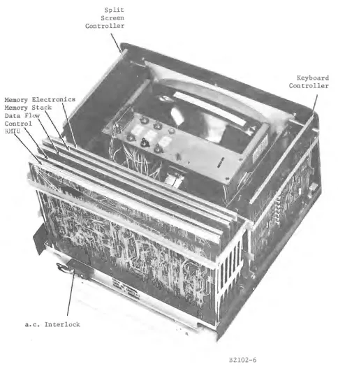
The Terminal Processing Unit is physically constructed of five printed
circuit boards which are identified as memory electronics, memory stack,
*'"
I N ~rogram Counter B:egister'l'
Memory Address Register"'
...
,. ... , MEMORY(2K core
and controJ.l'
II\
"'
~Accumulator B:egister !:!emory Data B:egister .-~ If\ ·.·.··.·-:-;.·-:-:-:-:-::::::;:;·;:;:; SPD-L,.-~~~--•'•'·~::~.>~IProgram
1 m Loader
..
SPD-T TapeCassette
Line
~ Register \II \II \I/
K
>i
~uxiliaryArithmetic
~
t
I I '
1
t,
·.
-I N T E R F A C E ;1:<
<
:>
SPD-P Printer C 0 N T R 0 L
.,f~
Character
~ ~!egister
I<
~ B:egistert'?
Computer Data Flow
..
,
$
REFRESH MODULE TIMING UNIT Condition Status Registert
\II
\IJArithmetic Unit
mm:t
:IJu:;ffiihnel
,,::,:::,:::::,,,,::c:::::::::,,,,,,,,,,.~ ,,,,,,'{::)••==::r,,,,,,,.,.
'k
,,,,
.,,
,,,,,,,v,:::::::;,,;:::;:::: ,,,,,, -·Display J
\
Figure 4-1. SPD 10/20 Stored Program Display System
memory boards have been combined functionally; the Data Flow has been
re-duced to show the register detail in a system concept. The functional units
that are contained on these boards have been identified to show the basic data
flow and to introduce the reader to the terminology used in Chapter V, Theory
of Operation. The illustration shows a Keyboard, SPD-P Printer, SPD-M
multiplexer, SPD-LProgram Loader and SPD-T Tape Cassette connected to
the Terminal. Each device except the SPD-L and SPD-T require a plug-in
Controller to interface with the Terminal. Figure 4-2 shows the printed
circuit board arrangement and identification.
4. 2. 2 Terminal Processing Unit
1. Computer Data Flow (See Figure 4-1)
Memory: The SPD 10/ 20 utilizes a ferrite core coincident-current
memory organized in a 3D-4 wire configuration. The memory
capacity is 2048 words of 16 bit length (referred to as a 2K x 16
memory). Physically, each bit plane consists of a 64 x 32 core
matrix. Sixteen planes are mounted on a circuit board in a 4 x 4
arrangement. The memory functional layout is discussed in
para-graph 4.
Memory Data Register (MDR): A 16-bit register which buffers
all data to and from the memory. The contents of this register
are also available to the Display Subsystem.
Memory Address Register (MAR): A 12-bit register which stores
the address of the memory byte. Control of this register is also
possible through the Display Subsystem.
Program Counter Register (PCR): A 12-bit register which
con-tains the address of the next instruction to be executed. The least
significant bit is always zero.
Accumulator (ACR): An 8-bit register which contains the data for
the output bus and receives data from the input bus. It is also the
primary arithmetic and logical register of the processor.
Cursor Register (CUR): A 12-bit register which controls the
position of the cursor on the display. It can also be used in
Memory Electronics
Memory Stack
Data Flow
a. c. Interlock
Split Screen
Controller
[image:48.612.57.541.89.630.2]B2102-6
Figure 4-2. Circuit Board Identification and Location
Keyboard
,,
I
Character Register (CHR): The least significant six bits of the
cursor register which represents the cursor location on a line.
Line Register (LIR): The most significant six bits of the cursor
register which represents the number of the line on which the cursor is displayed.
11
6 5
00CUR
Cursor Register Layout
Condition Status Register (CSR): This 3-bit register stores the
status of all arithmetic operations.
02 01 00
I
EQco
Negative (NG) Set if the most significant bit of the arith-metic unit (ARU) operation is 1.
Equal (EQ) Set if the result is zero after an Arithme-tic Unit or Auxiliary ArithmeArithme-tic Unit operation.
Carry Out (C) . • • Set on an overflow condition from AAU or ARU operation,
Arithmetic Unit (ARU): This 8-bit unit performs arithmetic and
logic operations such as add, subtract, and, or.
Auxiliary Arithmetic Unit (AA U): This 12-bit unit provides
capa-bility for+ 1, + 2, + 4, -1 and comparison operations on a word basis.
Input Data Bus (IDB): This 8-bit bus consists of eight lines which transfer data from an I/0 device to the accumulator (ACR).
Output Data Bus (ODB ): This bus consists of eight lines which
transfer data from the accumulator (ACR) to an I/0 device.
Peripheral Address Bus (PAB): This bus transmits the address
and function command for a selected peripheral directly to the
used to define the function to be performed by the peripheral device. The information is obtained as a decoded output from the Memory Data Register.
2. Control
The SPD 10/ 20 control electronics are contained on a single printed circuit board. Numerous control functions are provided by the interaction of system timing phases and extensive signal gating. A primary function is the decoding of the operation code and subsequent directing of the specified instruction. The State Counter and Real Time Clock are located on this board.
3. Refresh and Timing
The refresh and timing circuit board performs two major functions: one is the generation of a system timing chain; and the other is the processing and interfacing of data from the TPU to the CRT dis-play. Circuits are provided to compute the CRT line number and character position on a line.. The selected character is converted to a 7 x 10 dot matrix by the read-only memory which modulates the CRT video circuit and displays the character on the screen. The displayed character is refreshed at a rate that prevents image flickering.
4. CRT Display Unit
The CRT display is a commercially purchased (Sylvania) TV moni-tor. It is completely self-contained and has a viewing area that measures 9-1/2 inches wide by 7 inches high. In a single SPD 10/ 20 configuration, the display format consists of 30 lines of 64 characters each. In a dual SPD 10/ 20 configuration, both screens display 15 lines of 64 characters each.
4. 2. 3 Interface Control
The SPD 10/20 can accommodate a maximum of eight Controllers,
all under TPU control. Table 4-1 lists the Controllers by type, function and
external device controlled.
Table 4-1. SPD 10/20 Controllers, Related Functions and External Devices
Controller Keyboard Asynchronous Synchronous Split Screen Function
ASCII interface with SPD 10/ 20 keyboard. (Two required for auxiliary operation. }
(EIA} Standard RS-232-C inter-face for communicating with standard line modems. One controller for half duplex. Two controllers for full duplex. Operation is 50 to 2400 Baud.
{EIA} Standard RS-232-C inter-face for communicating with standard line modem. One con-troller for half duplex. Two controllers for full duplex. Operation is 1200 to 4800 Baud.
Used with Auxiliary Display to provide Master Display time sharing.
4. 3 ADDRESSING AND INSTRUCTION FORMATS
4. 3.1 Introduction
External Device
Keyboard
SPD-M Multi-plexer, Data-speed Service, Teletype, TWX, Telex, Honey-well Data Sta-tion, SPD-P Printer, Remote Load.
Univac DCT 2000, IBM 2780, RCA 70/740, Data-term, Remote Load.
SPD Auxiliary Terminal.
The purpose of this paragraph is to provide a fundamental discussion
of the addressing and instruction formats used with the SPD 10/20 Terminal.
Refer to the SPD 10/20 Programmers' Reference Manual for a detailed
dis-cussion of this subject plus a complete listing of instruction formats,
[image:51.612.67.551.173.546.2]4. 3. 2 Hexadecimal Notation
In programming the SPD 10/20, memory addresses and instruction
codes are listed in the hexadecimal notation. It is a convenience, like
short-hand, to express a code as four hexadecimal symbols rather than a string of
16 binary symbols (l's and O's).
Any positional number system can be defined by its base (radix). The
base is the number of unique symbols that can occupy a position in the number
system. For example, the binary system has two symbols (base 2); the octal
system has eight symbols (base 8); and the decimal system has ten symbols
(base 10). The hexadecimal system has 16 symbols, so it is a base 16 sys
-tern. The symbols are: O, 1, 2, 3, 4, 5, 6, 7, 8, 9, A, B, C, D, E and F
(see Table 4-2).
Table 4-2. Decimal, Binary and Hexadecimal Equivalents
Hexadecimal
Decimal Binary Symbol Spoken
0 0000 0 Zero
1 0001 1 One
2 0010 2 Two
3 OOll 3 Three
4 0100 4 Four
5 0101 5 Five
6 OllO 6 Six
7 Olll 7 Seven
8 1000 8 Eight
9 1001 9 Nine
10 1010 A Able
ll lOll B Baker
12 llOO C Charlie
13 llOl D Dog
14 ll 10 E Easy
15 llll F Fox
In converting from hexadecimal to decimal, the symbol represents
both a coefficient and its position in the number (the exponent of the base).
The exponent of the base (position) is determined by counting from right to
left. For example, convert the hexadecimal number 4F2 to its decimal
[image:52.612.98.506.332.602.2]4F2
=
4(162)+ F(l61)+ 2{160)=
4(256)+ 15(16) + 2(1)= 1024 + 240 + 2
=
1266The Enable Interrupts {ENB} instruction is presented as an example of the convenience of coding in the hexadecimal system.
115
12111
87 4 '
3
I
1
I
~I
Bit Number
:1l1lolo:ol
0 0 0lololo!o:
01
Binary CodeC 0 0 6 Hexadecimal Code
Charlie Zero Zero Six
4. 3. 3 Word Formats
The SPD 10/20 addressing and instruction word is composed of an odd/ even byte pair, containing eight bits each. The word can be accessed by
addressing either byte; however, for compatability, the address of the even byte should be used.
1 (
6
5 4Odd Byte
I
16 BIT WORDThere are three major instruction formats: 1. Non-memory reference
2. One word memory reference 3. Two word memory reference.
1. The non-memory reference instructions are a group of operations which contain their own data; therefore, they do not need to
2. The one word memory reference is an instruction in which a particular location in memory is fetched during the instruction cycle. If the resulting data is determined to be the effective data, the Terminal will operate on it during the execute cycle. 3. The two word memory reference only occurs when test jumps
or test input-output is desired. The data is arranged such that the first word is used for operating instructions while the sec-ond contains address information.
4. 3. 4 Instruction Class es
The SPD 10/20 provides a repertoire of 58 instructions including: 16 data manipulation
11 cursor control 20 test and/ or branch
6 input/ output 4 miscellaneous
1. Byte Class: An op code instruction dictating action on the byte at the effective address. Actions are:
Load Store Add Subtract
Compare And Or
2. Cursor Class: The data in the cursor register (line and character taken together) can be loaded with the word at the effective address, stored at the effective address, or compared to the effective
address.
3. Increment Class: The word at the effective address can be incre-mented by one, increincre-mented by two, or decreincre-mented by one. 4. Jump Class: Provides for an unconditional jump to the effective
word address or jump to a subroutine, in which case a return address is stored.
6. Immediate Class: The effective data is located in the odd byte of the instruction word.
7. Input/Output Class: Provides device attention to I/0 controllers and provides the necessary interface select and enabling data. Included in this class are Control, Read and Write with a condi-tional test for possible jump.
8. Operate Class: Enables a large majority of data movement within the Terminal's operating registers. Interface commands also form a part of this class.
4. 3. 5 Effective Address Calculation
An example of an effective address calculation is presented in this paragraph. The textual discussion is supported by diagrams of the instruc-tion words.
Prior to the discussion, it is necessary to explain the functional divi-sion of the core memory. Figure 4-3 shows the functional division of a memory bit-plane. Each plane contains 2048 locations (words). Information is trans-ferred in and out of the memory as complete 16-bit words: that is, the identi-cal core location in all 16 bit-planes. The memory is divided into eight
sectors, each of which contains 256, 16-bit words or 512 bytes. Each sector is divided into an upper page and lower page of 128 words each. The highest numbered sector (7) is labeled TOP; sector 6 is labeled TOP-1. A 44 byte reserved area is contained in sector 7. Hex bytes 000 through 77F are re-served for refreshing displayed data. The remaining area is used for program storage.
A discussion of a sample effective address calculation is presented below. The text is keyed to Figure 4-4 which shows the layout of the one-word memory reference instructions used in the operation. Bit
identifica-tion is as follows:
Bits 11 through 15: Bits 00 through 08:
Bit 10:
Opcode
Displacement (relative address) with defined sector
Words
HexAddress Bytes
2047 Upper Page
TOP EFF-EOO
-
EOOLower Page
1---4
-
·
-1791
TOP-1
DOO
DFF-COO-
coo
1535
5 00 BFF-AOO
-
-AOO1---11
...
- - - 1
-·
- -
-~..
4 900
~
..
1279
9FF-800
- 800
3 7FF-600
- - 600
2 SFF-400
-
-
-
- 4001 3FF-200
-
·
-
-
-
2000 lFF-000
[image:56.612.60.530.137.572.2]- -
-
- 00015 14
15 14
15 14
15 14
lo
p
CODE 13 12i
!OP CODE 13 12
OP CODE
ioP CODE
i
~ i
13 12
' '
!OP CODE \
1 ~
I
13 12
1
11
11
11
11
TO MAR
i
l
0 0 0 0 0 0 0 0 0' I
1
.·.., , Relative Addr1ess' I
: Within Secto.r
i
10 9 8 7 6 5 4 3 2 1 0
TO MAR
0 0 0 0 0 0 0 0 0 Relltivk Addr1ess:
·· w·1 1n ec o~ 'th" t S It l ; 10 9 8 7 6 5 4 3 2 1 0
• i J
Relative Address,
1
1
I ' I
l
Within Sector 19
MDR is Effective Address
10 9 8 7 6 5 4 3 2 1 0
Fetch Word From Memory
10
8
10
9 8
7 6
5 4 3 2 1 0 where a page= 1/2 a sectorTOP
TOP-1 If Current Sector TOP
Current Sector If Current is
Not TOP
Direct
Indirect
Upper Page
Lower Page
[image:57.612.69.548.66.688.2]Bit 9:
Bit 8:
Sector address 1
=
TOP sector0
=
Current sector if current sector -/- TOP0 = TOP-1 sector if current sector = TOP
Page identification (0
=
Lower page, 1 = Upper page}.Sample Effective Address Calculation (See Figure 4-4}
1. The sector bit (bit 9) is tested. If it is 1, the last sector of memory
(TOP) has been referenced. The address of the top sector, linked with the instruction's displacement field, is loaded into the Memory
Address Register (MAR). GO TO step (4).
2. If the sector bit is not 1, test to see if the current sector is TOP.
If so, the sector below TOP has been referenced (TOP-1). TOP-1 linked with the instruction's displacement field is loaded into the
MAR. GO TO step (4).
3. If the current sector is not TOP, then the current sector has been referenced. Combine the sector bits of the Program Counter
(PCR) with the instruction's displacement and load the result into the MAR. Note that the PCR still contains the address of the cur-rent instruction at this point.
4. The indirect bit (bit 10) is tested. If it is O, there is no indirect addressing, and the MDR contains the true effective address. The instruction execute cycle is entered which uses this address. The
least significant bit (LSB) of the effective address has been main-tained for use in byte instructions.
5. Indirect addressing is indicated. The MAR is used to fetch an in-direct address word from memory, which is loaded into the MDR.
If the indirect bit (bit 15) of this word is 1, continue by a GO TO
step (5).
If it is O, the MDR contains the true effective address.
The instruction execution cycle is entered, which uses this address.The LSB of the effective address has been maintained for use in
byte instructions.
4. 3. 6 Basic System Timing and Data Flow
The system timing is generated on the Refresh Module and Timing Unit
circuit board. The system operates on two cycles, each of which is divided into 20 equal increments or timing phases. The instruction cycle is first,
is fetched during timing phases 1 through 10 and decoded during timing
phases 11 through 20. During the execute cycle, the selected data is fetched
during timing phases 1 through 10 and is operated on during timing phases 11
through 20.
The processing of a specific instruction (Increment and Store) is
pre-sented as a typical example of system activity with respect to timing.
Obvi-ously, each instruction requires a different data path within the TPU;
how-ever, some operations follow the same pattern, such as Memory Data Register
strobe at time T4 and Program Counter Register update at time T 19.
Processing of Increment and Store Instruction
The purpose of an Increment and Store instruction is to retrieve data
in a specific memory location, add 1 to it, and return it to the memory.
Fig-ure 4-5 is a timing diagram for this operation.
Activity starts at time T4 when a memory data word is strobed into
the Memory Data Register (MDR). At the trailing edge of TS, the opcode
portion is decoded and saved in the Instruction Register so that during the
remainder of the operation the computer knows what it is supposed to do.
The address portion of the word is taken from the MDR and after Tl 1,
en-abled to the Auxiliary Arithmetic Unit (AA U) where zero is added to it, and
it is loaded into the Auxiliary Arithmetic Register (AAR) at Tl 7. At Tl 9,
the address is placed in the MAR, such that the MAR is pointed to the address
which it is desired to increment. At this point, the instruction cycle has
been performed and the execute cycle is entered.
Execute cycle time T4 enables the MAR Selected Data from the MDR
to the Auxiliary Arithmetic Unit where it is incremented by one, and at T?,
the result is placed in the Auxiliary Arithmetic Register. Also at T? the CSR
is set as required. At T9, the AAR data is placed in the MDR so that it can
be written back into memory. The line and character are not important unless
a cursor operation is involved. At this point, the data movement called for
has been performed. All that remains is to up-date the Program Counter
Unit where a +2 is added to it ( +2 because of byte orientation, two bytes per word). At Tl 7, it is enabled to the Auxiliary Arithmetic Register. At Tl 9
*"
I...
-.J
TIMING ~
MDR ARU
ACR
PCR
MAR
AAU
AAR
LIR
CHR
Inst
Reg,
CSR
INSTRUCTION CYCLE EXECUTE CYCLE
+
t
q
E
?: ?.
::
?.
!
~
~P
:
:
;g
!1.-.?.::-
!?
:
w~
:
~
:
?.
~§: 17
x~
::
¥?
gp.11
,&
&'J
ti
R
.
~i
t
i
t
!tllf
f
jt[q;i;ii
lf
jfi
fi
lt
i;
;ii;;
:Y
tl
~}
Wl
,;;
il
z;
B
;.
g
p
___ f:il
r:;i
r;1_ __________ _
~ - - - - = - - - ~ J w l
~ ~ ~ = = - - ~ R - .
Jwl
Jil
I
AAU:MDR+OI
f
AAU:MDR+ I AAU:PCR+l_____
__.r;,
r,;]
[71
rvl~--- rvl~--- rvl~--- rvl~--- rvl~--- rvl~--- rvl~--- rvl~--- rvl~--- rvl~--- rvl~--- rvl~--- rvl~--- rvl~--- rvl~--- rvl~--- rvl~--- rvl~--- rvl~--- rvl~--- rvl~--- rvl~--- rvl~--- rvl~--- rvl~--- rvl~--- rvl~--- rvl~--- rvl~--- rvl~---rvl~---rvl~---rvl~---rvl~---rvl~---rvl~---rvl~---1f°i41 ...
*
______
_
- - - ' 14
~
5
7 7
---
....___________________ _
(This strobe is a don't core)
*
LIR and CHRstrobed on Tl4 if instruction is increment and