Nanoscale Structure Dynamics within Electrocatalytic Materials
Cameron L. Bentley,*
Minkyung Kang, and Patrick R. Unwin*
Department of Chemistry, University of Warwick, Coventry CV4 7AL, U.K.
*
S Supporting InformationABSTRACT: Electrochemical interfaces used for sensing, (electro)catalysis, and energy storage are usually nano-structured to expose particular surface sites, but probing the intrinsic activity of these sites is often beyond current experimental capability. Herein, it is demonstrated how a simple meniscus imaging probe of just 30 nm in size can be deployed for direct electrochemical and topographical imaging of electrocatalytic materials at the nanoscale. Spatially resolved topographical and electrochemical data are collected
synchro-nously to create topographical images in which step-height features as small as 2 nm are easily resolved and potential-resolved electrochemical activity movies composed of hundreds of images are obtained in a matter of minutes. The technique has been benchmarked by investigating the hydrogen evolution reaction on molybdenum disulfide, where it is shown that the basal plane possesses uniform activity, while surface defects (i.e., few to multilayer step edges) give rise to a morphology-dependent (i.e., height-dependent) enhancement in catalytic activity. The technique was then used to investigate the electro-oxidation of hydrazine at the surface of electrodeposited Au nanoparticles (AuNPs) supported on glassy carbon, where subnanoentity (i.e., sub-AuNP) reactivity mapping has been demonstrated. We show, for the first time, that electrochemical reaction rates vary significantly across an individual AuNP surface and that these single entities cannot be considered as uniformly active. The work herein provides a road map for future studies in electrochemical science, in which the activity of nanostructured materials can be viewed asquantitative movies, readily obtained, to reveal active sites directly and unambiguously.
■
INTRODUCTIONTechniques that can resolve nanoscale structure−activity at complex electrochemical interfaces and ensembles are much needed in order to understand the behavior of functional nanostructured electrodes1,2 that have applications ranging from (electro)catalysis and energy storage3−6to biomedical and environmental sensing.7,8In this work, we demonstrate how a simple meniscus imaging probe, based on a single-channeled nanopipet (inner diameter,d≈30 nm), can be used to carry outsynchronous electrochemical/topographical imagingwith high spatial resolution to provide unprecedented views of electro-catalytic processes in action. This approach provides unambiguous quantitative information on the intrinsic activity of characteristic surface sites (e.g., step edge vs terrace sites on an extended surface and activity distributions within a single catalytic nanoparticle), directly highlighting structural controls on (electro)catalytic activity.
Among a limited set of techniques for mapping (electro)-chemical activity at the nanoscale,9−15scanning electrochemical probe microscopy (SEPM) methods are presently gaining attention.14,15The most commonly utilized SEPM technique, scanning electrochemical microscopy (SECM), has recently been employed to study the activity of electrocatalytic nanomaterials in the tens to hundreds of nm size range.16−19 However, for these applications and most others, the technique operates in a constant plane scanning mode with no positional feedback of the tip with respect to the surface of interest. Such measurements are difficult to implement and analyze (due to
piezoelectric positioner drift, etc.), and no topographical information is obtained. This limitation can be overcome to some extent through the use of dual redox mediators (one to image topography, the other to measure activity)20 or the integration of SECM with other scanning probe techniques such as atomic force microscopy (AFM)21,22or scanning ion conductance microscopy (SICM).23−26 However, fabricating reproducible nanoelectrode probes is nontrivial and time-consuming, and this is even more complicated when multi-channel probes are employed.15
It is important to point out that in SECM substrate activity is measuredindirectly, often by monitoring the spatially depend-ent fluxes of reactant, product, or intermediates from the substrate at the tip,15−18 and thus suffers from diffusional broadening, exacerbated at the nanoscale, where neighboring sites on a surface may interact (diffusional cross-talk). This makes “single-entity” activity mapping within an ensemble of active materials very challenging. Furthermore, the need to immerse the entire surface during measurement and the long scan-times that are used (typically at least several tens of minutes for a single image frame) complicates sample preparation and renders the technique susceptible to surface-aging effects at the sample and the tip, induced by electrolyte exposure and the electrochemical process that has to be run for a long time.
Received: September 1, 2017 Published: October 23, 2017
Article
pubs.acs.org/JACS
License, which permits unrestricted use, distribution and reproduction in any medium, provided the author and source are cited.
Downloaded via 137.205.202.197 on July 31, 2019 at 16:05:07 (UTC).
In contrast, in scanning electrochemical cell microscopy (SECCM) and related droplet cell-based imaging techniques, the electrochemical properties of a substrate electrode surface are probeddirectly and locallywith integrated probe positional feedback.27,28Electrochemical measurements are confined to an area on a surface defined by the droplet (meniscus) from the end of a pulled glass or quartz capillary, with probe (tip) diameters typically in the hundreds of nm29,30toμm31,32range. Structure−function problems of many different classes of materials have been resolved with SECCM-based meth-ods.30,33−36 Recent studies have shown the strength of the voltammetric“hopping”mode,36−38where electrochemicalflux data over large potential ranges (>1 V) can be constructed through data acquisition of a full cyclic (or linear-sweep) voltammogram at each pixel, although lengthy scan times are needed to acquire such data.
The work reported herein addresses new domains in high-resolution electrochemistry, such as probing the full current− voltage relationship of elementary nanoscale sites on surfaces, andwithin individual entities(nanoparticles, NPs), achieved by great advances in the spatial resolution and image acquisition rates possible with electrochemical imaging. We report synchronous maps of topography (height resolution of better than 2 nm) and electrochemicalflux movies with hundreds of frames (2500 pixels/frame), obtained in just minutes. The technique is first benchmarked by investigating the hydrogen evolution reaction (HER) on MoS2, a promising earth-abundant electrocatalyst, which has recently been investigated with SECCM.36Major new insights on the intrinsic activity of edge and basal planes are unveiled, afforded by the excellent spatial resolution achievable with thefine nanopipet probe (d≈ 30 nm). Furthermore, subparticle activity variations are
demonstrated for thefirst time with any SEPM method, with the kinetics of hydrazine oxidation shown to vary significantly across the surface of individual AuNPs. Subentity measure-ments in electrochemistry have only recently been realized and have been confined to optically active molecules.9−13 While these methods are powerful, the method described herein is generally applicable to any electrochemical process.
■
RESULTS AND DISCUSSIONSingle-Channel SECCM: Operating Principles. Salient experimental details are given in theExperimental Section, but for clarity of understanding, key features of the single-channel SECCM protocol utilized herein are outlined. The instrumen-tation and working principles of the SECCM setup are shown schematically in Figure 1a. A single-channel nanopipet probe [transmission electron microscopy (TEM) image shown inset in Figure 1a] with surface current (isurf) positional feedback (detailed below) was employed. This instrumental set up is greatly simplified compared to the conventional dual-channel SECCM set up,27,28,39 only requiring x−y−z piezoelectric positioners, a current follower (electrometer), a waveform generator (digital herein), and a data acquisition system (FPGA card herein). In this work, SECCM has been operated in the voltammetric “hopping” mode regime,36−38 where the nano-pipet probe was approached to the surface of interest at a series of predefined locations in a grid, and, upon each meniscus landing, a voltammetric experiment (cyclic/linear-sweep or potential-step waveforms) was carried out, building up a dynamic electrochemical“map” of the substrate.
[image:2.625.111.514.62.316.2]Examples of thez-position, applied potential (Eapp), andisurf synchronously recorded at high frequency, as a function of time, during a single“hop”of a voltammetric SECCM scanning
Figure 1.(a) Schematic of the general procedure for voltammetric hopping mode SECCM with a single-channel nanopipet probe. In this setup, a voltage of−Eappwith respect to ground is applied at the quasi-reference counter electrode (QRCE) in the nanopipet barrel to control the working
electrode potential (Eapp), and the working electrode current (isurf) is measured.isurfalso serves as a feedback signal to detect meniscus contact with
the surface during probe approach. The arrows show the movement of the nanopipet probe along the surface (shown inset). Also shown in the inset is a TEM image of the end of a representative nanopipet probe (the scale bar indicates 40 nm). (b) Example plots of (i)z-position, (ii)Eapp, and (iii) isurfas a function of time, recorded simultaneously during a single approach to a MoS2substrate with a nanopipet containing 100 mM HClO4at an
acquisition rate of ca. 0.25 s per pixel.
experiment are shown inFigure 1b. During the initial approach (1 inFigure 1b), Eapp(termed the approach voltage, Ea) was chosen to be sufficient to drive the reaction interest (HER in the example in Figure 1b) at the substrate surface upon meniscus landing to generate a reliable current signal for positional control, without the probe making physical contact. When the meniscus made contact with the substrate surface, a two electrode electrochemical cell was formed and a reductive transient in isurf resulted due to the reaction at the substrate (working electrode) within the confined area of the droplet cell. Thez-approach halted immediately upon detecting a user-set threshold current (isurf≈ −0.95 pA, herein), andEappswitched to the initial potential, causing an oxidative transient in isurf attributable to double-layer charging current (2inFigure 1b). After a predefined hold-time (10 ms in Figure 1b), an Eapp−t waveform was applied (linear sweep at a voltammetric scan rate, ν, of 10 V s−1 in Figure 1b) and i
[image:3.625.324.564.128.371.2]surf was recorded simultaneously (3 in Figure 1b). After holding at the final potential (4inFigure 1b) for a predefined hold time (5 ms in Figure 1b), the probe retracted andEappswitched back to the initial approach value for the next hop (5 inFigure 1b).
The procedure outlined above repeated at each pixel of the scan andisurf at a givenEappwas plotted as a function of x−y coordinate to produce“electrochemical maps”of the substrate. The individual isurf−Eapp “frames” were then combined to produce spatially resolved electrochemical movies, which visualize the activity of the surface over a large potential range. In addition, the final z-position of the piezoelectric positioner during approach (i.e.,3inFigure 1b−i) was plotted as a function ofx−y coordinate to produce a high-resolution topographical image of the scan area. Herein, this methodology, combined with the use of a fine, single channeled nanopipet probe (d ≈ 30 nm), has enabled fast, high-resolution simultaneous topography/activity mapping of catalytic nano-materials. The two electrocatalytic systems considered below, (i) MoS2, a promising earth-abundant electrocatalyst for the HER,40 and (ii) metallic NPs adhered to a carbon support, which is widely utilized in a range of catalytic applications4,5 (e.g., [N2H5]+oxidation herein), serve to demonstrate the wide applicability of the technique.
HER at MoS2: Basal vs Edge Plane Activity. MoS2has attracted considerable interest in a range of (electro)chemical applications, for example, as an abundant and low-cost alternative electrocatalyst to platinum for the HER,eq 1.40,41
+ →
+ −
2H 2e H2 (1)
In a recent study from our group,36 correlation of spatially resolved SECCM measurements with structural information from scanning electron microscopy (SEM) and AFM demonstrated unequivocally that the HER is greatly facilitated at the edge plane (e.g., surface defects such as step edges) relative to the basal plane, which possessed activity comparable to polycrystalline Co, Ni, Cu, and Au. Using a conventional two-barreled probe (d≈600 nm) to generate a 2025 pixel map (45×45, 1μm spatial resolution) at a rate of ca. 10 s per pixel, it was demonstrated how individual linear sweep voltammo-grams (LSVs) could be extracted and analyzed semiquantita-tively to reveal a Tafel slope of∼120 mV/decade and exchange current densities (J0) of 2.5×10⁻⁶and∼1×10⁻⁴A cm−2on the basal and edge planes (i.e.,J0,EP/J0,BP≈40), respectively. In order to benchmark the single-channel SECCM approach highlighted inFigure 1a, this process was investigated, but with time-scale and spatial resolution improvements of ca. 40- and
400-fold, respectively, to reveal significant new insights into nanoscale structure−function in this class of material.
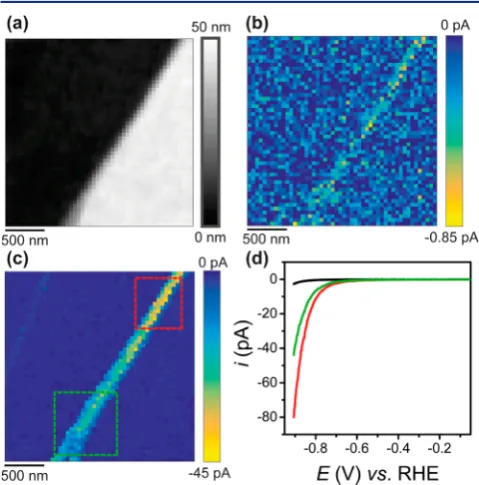
An important aspect of this technique is that the probes used are easily visualized by TEM after experiments. The probe used to obtain the MoS2 activity/topography data in Figure 2 is
shown in Figure S1a. The topographical map in Figure 2a obtained directly by SECCM easily reveals a ca. 40 nm high step traversing the scan area from top to bottom. As the theoretical thickness of a monolayer of MoS2is ca. 0.68 nm,42 this feature is made up of tens of MoS2 layers. The topographical line-scan profiles taken across the step, shown inFigure S2, show that the morphology of the feature actually changes from a single multilayer step at the top (41 nm, red trace) to two smaller multilayer steps at the bottom (20 and 21 nm in height, blue trace). It needs to be emphasized that the high-resolution topographical image shown in Figure 2a has beenproduced directly using SECCM(z-positional data) and yet is comparable in quality to previously reported AFM topo-graphical images obtained on similar sized (step edge) features.36This is obviously a major advantage of the approach outlined herein: high-resolution topographical and electro-chemical (vide infra) images are obtained synchronously in a single scanning experiment. Thez-height resolution achievable with the instrumental set up outlined inFigure 1is considered below.
Figure 2. (a) Topographical and (b, c) spatially resolved electro-chemical maps (2500 pixels over a 2.5×2.5μm scan area, 400 pixels μm−2) obtained with the voltammetric hopping mode SECCM
protocol (Figure 1), visualizing HER activity on a cleaved MoS2
surface. The nanopipet probe (d ≈ 30 nm, TEM image shown in
Figure S1a) contained 100 mM HClO4. The electrochemical maps are
for (b)−0.507 and (c)−0.857 V vs RHE (seemovie S1for the full potential range with 451 frames). (d) Average LSVs obtained on the basal plane [black trace, dark blue areas in (c)] and surface defects (steps) of∼21 nm [green trace, indicated by the green box in (c)] and ∼41 nm in height [red trace, indicated by the red box in (c)]. Experimental parameters were as follows:ν= 1 V s−1, scan time (ts) of
43.9 min (ca. 1.05 s per pixel) andEa=−0.907 V vs RHE. The data
presented in (a−c) are not interpolated.
A spatially resolved LSV-SECCM movie of the scan area is shown in movie S1. The movie consists of 451 image frames [i.e., 1 image every 2 mV, total scan time (ts) = 43.9 min], and each pixel (50×50 = 2500 in total) represents an individual (LSV examples shown inFigure S3) in the 2.5×2.5μm scan area (pixel density = 400 pixelsμm−2). The map was obtained at a rate of ca. 1.05 s per pixel, which is further improved upon below. Two individual frames from the movie, at potentials of
[image:4.625.325.566.211.418.2]−0.507 and −0.857 V vs the reversible hydrogen electrode (RHE), are shown in parts b and c, resepectively, ofFigure 2. Through correlation of the electrochemical maps with the topographical data inFigure 2a, it is clear that while the basal plane possesses uniform activity, the kinetics of the HER are enhanced at the site of the surface step defect (i.e., edge plane). In contrast to our previous study,36where only a single pixel was collected along a line across a step edge, herein multiple pixels have been collected laterally across the region of surface defect, indicating that the activity of the edge plane (i.e., exposed at the surface defect) has been probed more directly. In order to illustrate this point, a schematic showing the meniscus cell landing on a “large” (i.e., ca. 40 nm) step-edge feature has been included inFigure S4. It should be noted that the geometry (dimensions) of the large step-edge feature shown in the schematic was derived from az-height line-scan profile obtained directly in the SECCM scan, as shown in Figure S2b. Clearly, the proportion of exposed edge-plane within the meniscus cell probed area (droplet footprint) will scale with the size (height) of the surface defect and will be reflected in the current−voltage relationship at each pixel, as discussed below.
In Figure 2c, there is a clear gradient in the activity enhancement along the defect from top-to-bottom, due to the change in morphology from a single multilayer step (ca. 41 nm high, seeFigure S5) to two smaller multilayer steps (ca. 20 and 21 nm high). This is also evident in a histogram ofisurf(atEapp =−0.907 V vs RHE) as shown inFigure S6, where there are three distinct regions in the distribution, corresponding the basal plane and surface defect sites of ca. 21 and 41 nm in height. It is particularly clear fromFigure S6that the basal plane possesses a very uniform activity, with an averageisurfvalue of
−2.8± 0.7 pA (one standard deviation,N = 2244) at Eapp =
−0.907 V vs RHE. If point defects (e.g., sulfur vacancies), are responsible for the HER catalytic activity of the basal plane (2H phase), as has been proposed,43then these data indicate that the distribution would have to be highly uniform on the length scale (fewμm2) considered herein.
Average LSVs obtained on the basal plane (black trace) and along the major surface defect (green and red traces) spanning the scan area are shown inFigure 2d. Evidently, the raw LSV data are of excellent quality (example individual LSVs are also shown inFigure S3), clearly reflecting the activity enhancement seen in the electrochemical maps (Figure 2b,c). It is worth noting that the enhancement in catalytic current scales almost quantitatively with the size of the surface defect site, withisurf values of ca.−18 and−34 pA measured on the∼21 and∼41 nm step features, respectively (i.e., green and red box, respectively, in Figure 2c) at Eapp = −0.857 V vs RHE. Furthermore, the current densities (J) are very high, ca.−85 and−2700 mA cm−2 on the basal and edge planes atEapp =
−0.857 V vs RHE, respectively (values that would be impossible to achieve on this material with any other technique). The magnitude of the Jand the ratio of JEP and JBP are consistent with what was reported in our previous
study.36 These observations indicate that this ultrasmall scale meniscus (droplet) cell is relatively stable, with minimal distortion or spreading, even on the topographically challenging step edge features.
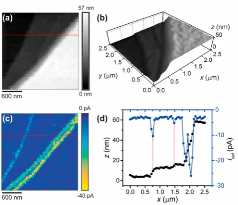
HER at MoS2: Pushing the Limits of Spatial Resolution and Acquisition Rate.InFigure 2, the approach (0.4μm at 5 μm s−1), retract (0.4μm at 10μm s−1), and lateral movement (0.05μm at 3μm s−1) take ca. 80, 40, and 17 ms, respectively, on each hop, which is insignificant compared to the time taken to obtain the LSVs, 900 ms (0.9 V at 1 V s−1). Thus, in order to improve the overall scanning time, aνof 10 V s−1was applied; the results are shown inFigure 3. The topographical map in
Figure 3a reveals a series of features (surface defects) with sizes of ca. 8, 2, and 43 nm (line-scan profiles shown inFigure S7), from left to right, respectively. The smallest feature (defect), of just 2 nm, which is more obvious in the 3D plot shown in Figure 3b, is a step edge that is likely made up of a few (2 or 3) MoS2layers. It can be easily seen, with excellent signal-to-noise. This again reinforces the strength this technique: it provides true nanoscale resolution for synchronous topographical/electro-chemical imaging.
A spatially resolved LSV-SECCM movie of the scan area is shown inmovie S2. The movie is made up of 384 image frames (i.e., 1 image every 2.6 mV), with each frame comprised of 2500 pixels, at a density of 400 pixelsμm−2. The map took ca. 10.6 min to complete, corresponding to pixel (resolved in space) and frame (resolved inEapp) acquisition rates of ca. 0.25 s per pixel and 1.65 s per frame, respectively. It should also be noted that if only a single applied potential is of interest, a
Figure 3. (a, b) Topographical and (c) spatially resolved electro-chemical maps (2500 pixels over a 2.5×2.5μm scan area, 400 pixels μm−2) obtained with the voltammetric hopping mode SECCM
protocol (Figure 1), visualizing HER activity on a cleaved MoS2
surface. The 3D topographical map in (b) is presented in an aspect ratio of 1:1:10 (x/y/z). The nanopipet probe (d≈30 nm, TEM image shown inFigure S1a) contained 100 mM HClO4. The electrochemical
map is for−0.857 V vs RHE (seemovie S2for the full potential range with 384 frames). (d)z-Position (black trace) andisurf(blue trace) line
scan profiles of the area indicated by the red dashed line in (a) and (c). Experimental parameters were as follows:ν= 10 V s−1,ts= 10.6 min
(ca. 0.25 s per pixel), andEa=−0.907 V vs RHE. The data presented
in (a) and (c) are not interpolated.
potential-step (chronoamperometric) waveform can be applied, as demonstrated inFigure S8.
An individual frame from movie S2, obtained at an Eappof
−0.857 V vs RHE, is shown in Figure 3c. The quality of the image is comparable to that obtained at the slowerν(1 V s−1, seeFigure 2c), again showing enhanced HER kinetics at the surface defect sites (step edges). It is worth noting that the fact that an area of basal plane is observable between the two closely spaced but large multilayer steps (i.e., see the blue trace in Figure S7) in the activity map shown in Figure 3c again indicates that the meniscus (droplet) cell is stable in these experiments, with minimal distortion or spreading over the relatively large surface features. Finally, the line-scan profiles of topography andisurfin Figure 3d also demonstrate the strong coincidence between the surface features and HER activity, with the activity scaling with step height, as noted above.36
[N2H5]+Oxidation at AuNPs: Probing Heterogeneous Activity within Individual NPs. We now turn to catalytic AuNPs electrodeposited on a catalytically inert glassy carbon (GC) support (see theExperimental Section) and consider the electro-oxidation of hydrazine in acidic media,eq 2.44
→ + +
+ + −
[N H ]2 5 N2 5H 4e (2)
As shown in the SEM image inFigure 4a, they are irregularly shaped secondary particles (ca. 300 to 400 nm diameter) resulting from the aggregation of smaller (primary) Au clusters. In order to find an area of the support surface for electrochemical imaging, an 8 × 8 μm topographical map (0.1 μm hopping distance, shown in Figure S9) was
constructed using a standard hopping mode protocol, in which the probe (Figure S1b) was retracted immediately upon detecting the surface. The map is remarkable in being able to pinpoint primary AuNPs (indicated by arrows in Figure S9a) that barely show up in the SEM image (Figure S9b). After selecting a suitable area to study (marked as a red box inFigure S9), a voltammetric hopping mode SECCM was carried out (scan rate of 1 V s−1) to construct spatially resolved synchronous topographical and electrochemical maps, as shown in parts b and c, respectively, ofFigure 4.
The topographical map in Figure 4b (and shown in 3D in Figure S10) revealsfive AuNPs in the scan area (labeled 1−5 in the plot), in accordance with the SEM image shown inFigure 4a. The shape of the particles in the SECCM topographical image (Figure 4b) mirror the overall morphology revealed by SEM (Figure 4a). Also evident inFigure 4b are small scratches and wells in the GC support surface (arising from electrode polishing), which correspond well with the features visible from SEM imaging (Figure 4a). Again, this is a testament to the high-quality of the topographical images achievable with the voltammetric hopping mode SECCM set up shown inFigure 1, as these features are typically only a few nm deep. Similarly, high-quality topographical images of PtNPs on a GC support were also produced using this method, as shown inFigure S11. A spatially resolved LSV-SECCM movie from the scan area is shown inmovie S3. The movie is made up of 151 image frames (i.e., 1 image every 5 mV), with each frame composed of 2880 pixels, at a density of 400 pixelsμm−2, obtained at a rate of ca. 1.04 s per pixel. Through comparison of movie S3 with the topography map in Figure 4b, it is clear that the electro-oxidation of [N2H5]+[seeeq 2]“switches on”at the surface of the AuNPs at ca. 0.9 V vs RHE, whereas the carbon support remains homogeneously inactive throughout the entire potential range (0.615−1.365 V vs RHE), as expected, given the relative inactivity of carbon electrodes for this reaction.38,45 An individual frame of the movie, for a potential of 1.35 V vs RHE (i.e., under mass-transport control, see below) is shown in Figure 4c and highlights this contrast.
One can perform many analyses with these data. For example, particle-average LSVs for each of the five individual AuNPs can be produced and compared, as inFigure 4d. The average LSVs were extracted exclusively from pixels located on top of the particles (for reasons explored below) and exhibit the classical sigmoidal shape characteristic of (near) steady-state voltammetry, with a steady-state transport-limited current (ilim) of ca. 23 pA. This mass transport current is mainly due to diffusion but is modified by the electricfield at the end of the nanopipet.46On average, the AuNPs in the scan area possess slightly different activities for [N2H5]+ oxidation (the voltammetric half-wave potential, E1/2 varies by ca. 20 mV), increasing in the order (5) < (1)≈(3)≈(4) < (2) (individual particles labeled inFigure 4b). It is worth noting that the order of increasing activity does not correlate to the order in which the particles were scanned (i.e., the scan started andfinished in the bottom-left and top-right corners, respectively, in Figure 4c). Considering this, and the fact that E1/2 is comparable to what has been reported under similar mass transport conditions,45 it is clear that producing and maintaining a
“clean”catalytic surface is not an issue. It should also be noted that during meniscus landing the substrate surface is transiently biased at a strongly reducing potential (Ea=−0.835 V vs RHE inFigure 4), which has an in situ “surface cleaning” effect in electrocatalytic studies.32,36
Figure 4. (a) SEM image of AuNPs, electrodeposited on a GC support. (b) Topographical and (c) spatially resolved electrochemical maps (2880 pixels over a 3× 2.4 μm scan area, 400 pixelsμm−2) obtained with the voltammetric hopping mode SECCM protocol (Figure 1), visualizing the electrocatalytic oxidation of [N2H5]+on the
surface of AuNPs. The nanopipet probe (d ≈ 30 nm, TEM image shown inFigure S1b) contained 12.3 mM (N2H5)HSO4and 100 mM
HClO4. The electrochemical map in (c) is for 1.35 V vs RHE (see
movie S3for the full potential range with 151 frames). (d) Average
LSVs obtained from particle 1 (orange trace); particle 2 (red trace); particles 3 and 4 (blue trace); particle 5 (green trace); and GC (black trace). The individual AuNPs to which these LSVs relate are labeled in (b). Experimental parameters were as follows:ν= 1 V s−1,ts= 49.9
min (ca. 1.04 s per pixel), and Ea= −0.835 V vs RHE. The data
presented in (b) and (c) are not interpolated.
Inspecting the image in Figure 4c, lower ilim values are observed around the edges of the AuNPs compared to the top surface, which could be due to some distortion of the meniscus or minor droplet spreading onto the inactive GC support in these areas. This is consistent with the fact that the electrochemical footprint (see Figure 4c) is slightly larger than the topographical footprint (see Figure 4b). A similar observation was also made when investigating the HER on PtNPs, as shown in Figure S11. The slight instability of the droplet cell at and around the edges of the AuNPs was further confirmed by taking perpendicular line-scans of topography and isurfacross a particle and comparing them forEapp= 1.35 V vs RHE, as shown in Figure 5. Evidently, in both the x and y
direction, relatively constant ilim values are observed at pixels situated on top the AuNP (ca. 23 pA) compared to lower values at and around the edges. This is unsurprising, given the severe curvature on the edges of the AuNPs (on the scale of the droplet cell). In spite of this topographical variation, as demonstrated above, electrochemical data collected on top of the particles is amenable to further analysis.
[image:6.625.385.500.64.423.2]From movie S3, it clear that there are large variations in activity within each AuNP (i.e., at theintraparticle level), with local areas of high activity within each particle. This can be attributed to the fact that the [N2H5]+ electro-oxidation reaction is crystallographic orientation dependent5,37,44 and the AuNPs comprise nonfaceted aggregates of Au clusters (see Figure 4a). The subparticle reaction mapping that is possible with this technique was further explored for a single AuNP studied in isolation atEapp= 1.15 V vs RHE (i.e., nearE1/2), as shown Figure 6. Comparison of the topographical map in Figure 6a and the electrochemical maps inFigure 6b andmovie
S4reveals the strong spatial-dependent electrocatalytic activity. It should be noted that in order to discount any influence of slight variations in the droplet-cell morphology on the electrochemical data (i.e., ilim varied by ca. ± 10% for the pixels considered below), normalized surface current (isurf/ilim) is considered inFigure 6andmovie S4. This small variation has no influence on the deductions vis-a-vis subparticle activity.̀
[image:6.625.74.298.218.484.2]The LSVs extracted from four areas on top of the AuNP (pixels indicated in Figure 6a) are shown in Figure 6c. Evidently, there is a significant variation in electrocatalytic activity across the AuNP top surface, with E1/2 ranging from 1.08 to 1.14 V vs RHE in the presented LSV plots. Notably, while at the single-entity level, on average, all of the five particles investigated inFigure 4possessed comparable catalytic activity (see Figure 4d) at the subnanoentity (i.e., sub-NP) level, significant intra-NP activities are revealed. A replicate
Figure 5.(a) Topographical map of AuNP 2 (data fromFigure 4b, above) obtained with the voltammetric hopping mode SECCM protocol. Experimental details are available in the caption ofFigure 4. (b)y- and (c)x-direction line scan profiles ofz-position (black traces) andisurf(red and blue traces), obtained at an applied potential of 1.35
V vs RHE (i.e., under mass-transport control).
Figure 6.(a) Topographical and (b) spatially resolved electrochemical maps (400 pixels over a 1 × 1 μm scan area) obtained with the voltammetric hopping mode SECCM protocol (Figure 1), visualizing the electrocatalytic oxidation of [N2H5]+on the surface of an AuNP.
The nanopipet probe (d≈30 nm, TEM image shown inFigure S1b) contained 12.3 mM (N2H5)HSO4 and 100 mM HClO4. The
electrochemical map in (b), normalized with respect toilim(i.e.,isurf/ ilim), is for 1.15 V vs RHE (seemovie S4for 221 image frames over the
full potential range). Pixels collected on the GC surface were normalized with the AuNP surface average ilim (ca. 25 pA). (c)
Normalized LSVs collected at the individual pixels labeled in (a). Experimental parameters were as follows:ν= 1 V s−1,ts= 9.7 min (ca.
1.45 s per pixel) andEa=−0.835 V vs RHE. The data presented in (a)
and (b) are not interpolated.
measurement on the same isolated AuNP, as shown inFigure S12, confirmed that the areas of high/low catalytic activity (i.e.,
“hot” and“cold” spots) arefixed in position, highlighting the general reproducibility of this method.
The only previous reports of subnanoentity (i.e., sub-NP) activity mapping have relied on super-high-resolution optical imaging techniques utilizing surface-enhanced Raman scattering or surface-enhancedfluorescence to infer on (electro)chemical reactivity at the subentity level, within nanomaterials of similar size (hundreds of nm) to those studied herein.9−13 While powerful, they are restricted to certain probe molecules and, separately, require supplementary techniques to characterize morphology (e.g., electron microcopy). The approach presented herein (Figure 1) is more generally applicable to any electrochemical system. It should be noted that there might be further scope to improve the spatial resolution achievable with SECCM, with single-barreled quartz laser pulled nano-pipets of sub-10 nm diameter being reported elsewhere, although such probes have never been used for imaging of any kind.47
■
CONCLUSIONSIn conclusion, single-channel SECCM, deployed in a voltammetric hopping mode regime, opens up new prospects for direct topographical/electrochemical imaging of nanoma-terials at the subentity level. Topographical (z-height) and electrochemical (i−E) data are collected synchronously to construct images (maps) which easily resolve step-height features as small as ca. 2 nm (e.g., two- to three-layer step edge on MoS2) on planar surfaces, at rates as fast as 0.25 s per pixel or 1.65 s per image frame, to create potential-resolved electrochemical activity movies with hundreds of images in a matter of minutes. The basal plane of MoS2 (2H phase) was shown to possess highly uniform HER-activity overμm length-scale regions, while surface defects (i.e., few to multilayer step edges) gave rise to morphology-dependent (i.e., height-dependent) enhancements in catalytic activity. Individual AuNPs, electrodeposited on a GC support, were, on average, shown to possess comparable activities toward the oxidation of [N2H5]+(i.e., at the single-nanoentity level). By contrast, at the subnanoentity (e.g., sub-NP) level, individual LSVs collected within a single AuNP exhibited strongly spatially dependent activity toward [N2H5]+ oxidation. These exemplar systems pave the way for a future in electrochemistry in which the activity of nanostructured electroactive materials can be viewed directly and related to underlying structure through electro-chemical movies.
Although the method has been applied exclusively to subentity reactivity mapping with electrocatalytic nanomateri-als, such an approach would also be applicable to otherfields of materials science. Moreover, beyond imaging, the versatility of mobile meniscus cells is fast advancing, for example, as tools for surface nanofabrication48,49 and the creation of nanopores in surfaces,50and the advances herein on the use of the smallest meniscus probes should impact significantly on thesefields.
■
EXPERIMENTAL SECTIONChemical Reagents and Electrode Materials. Perchloric acid
(HClO4, Sigma-Aldrich, 70%), hydrazine sulfate ([N2H5][HSO4],
Sigma-Aldrich,≥99%), potassium tetrachloroaurate (KAuCl4,
Sigma-Aldrich, 99.995%), and potassium hexachloroplatinate (K2PtCl6,
Sigma-Aldrich,≥99.99%) were used as supplied by the manufacturer.
All solutions were prepared with deionized water (Integra HP, Purite, U.K.), which had a resistivity of 18.2 MΩ·cm (25°C).
The naturally occurring molybdenite (MoS2) crystal (previously
shown to be the semiconducting 2H phase36) was purchased from Manchester Nanomaterials Ltd. (U.K.). Prior to use as an electrode material,flakes of MoS2werefixed in place using copper SEM tape on
a glass microscope slide and mechanically cleaved using the“ scotch-tape method”.51In order to avoid possible issues arising from ohmic resistance (through bottom-contact), the freshly cleaved MoS2 flakes
were electrically connected through top-contact with conductive copper SEM tape. The glassy carbon (GC) substrate was purchased from HTW-Germany and polished with an aqueous slurry of 0.05μm Al2O3 (Buehler, U.S.A.) prior to use. The AuNPs were
electro-deposited onto the GC substrate from a 0.5 mM KAuCl4 in 0.1 M
HClO4plating solution by applying a potential of 0 V vs Ag/AgCl (3
M KCl) for 3 s, followed by 0.5 V vs Ag/AgCl for 30 s. The PtNPs were electrodeposited onto the GC substrate from a 1 mM K2PtCl6in
0.1 M HClO4plating solution by applying a potential of−0.4 V vs Ag/
AgCl (3 M KCl) for 150 s. The palladium−hydrogen (Pd−H2)
quasi-reference counter electrode (QRCE) was prepared by cathodic polarization of a Pd wire (0.125 mm diameter, Goodfellow, 99.95%) in a 0.1 M HClO4solution. Field-emission SEM images of the NP
ensembles were obtained with a GeminiSEM 500 scanning electron microscope (Zeiss, Germany), at an acceleration voltage of 3 kV, with an InLens detector. The QRCE potential was calibrated against a commercial saturated calomel electrode (SCE) after every experiment, which has a potential of +0.241 V vs the standard hydrogen electrode (SHE).52
Electrochemical Measurements. The electrodeposition
experi-ments were performed in a three-electrode format with an Ag/AgCl (3 M KCl) reference electrode and platinum wire (Goodfellow, U.K.) auxiliary electrode on a CHI-730A potentiostat (CH Instruments, U.S.A.). All other electrochemical experiments were carried out in the SECCM format on a home-built electrochemical workstation.28,39 In this setup (shown schematically in Figure 1), a single-barreled nanopipet probe wasfilled with electrolyte solution and mounted on az-piezoelectric positioner (P-753.3CD, Physik Instrumente). The tip of the nanopipet probes were circular in shape, with an internal diameter of ca. 30 nm (shown inFigure S1). A Pd−H2wire placed in
the barrel of the nanopipet, through the back, served as a QRCE. The nanopipet was positioned above the surface of interest using micropositioners for coarse movement and an xy-piezoelectric positioner (P-622.2CD, Physik Instrumente) for fine movement. During approach, isurf was used as feedback to detect when the
meniscus at the end of the nanopipet had made contact with the working electrode surface. The threshold current herein was ca. 0.95 pA. The nanopipet itself did not contact the substrate. Electrochemical (voltammetric) measurements were performed in the confined area defined by the meniscus (droplet cell) created between the tip and substrate.
Electrochemical measurements at the substrate (working electrode) were made using a linear-sweep voltammetric“hopping”regime.30,37,38 In brief, as shown schematically in Figure 1, the nanopipet was approached to the surface of interest at a series of predefined locations in a grid and, upon each landing, a LSV measurement was carried out, building up a voltammetric“map”of the substrate. Thefinal position of thez-piezoelectric positioner at approach was also used to build up a topographical image of the substrate synchronously (detailed below). The hopping distance (i.e.,xyspatial resolution) between each pixel was 50 nm.
The SECCM cell and all piezoelectric positioners were placed in an aluminum Faraday cage equipped with heat sinks and vacuum panels to minimize noise and thermal drift. The Faraday cage was installed on an optical table (RS2000, Newport, U.S.A.) with automatic leveling isolators (Newport, S-2000A-423.5). The QRCE potential was controlled (with respect to ground) and the substrate (working electrode, common ground) current was measured using a home-built electrometer. The current was measured every 4 μs, which was averaged 65 or 257 times, to give data acquisition rates of 260 and 1028μs at voltammetric scan rates of 10 and 1 V s−1, respectively (i.e.,
1 data point every 2.6 or 1.028 mV, at 10 and 1 V s−1, respectively). During the chronoamperometric and conventional scan-hopping experiments, the current was measured every 4μs and averaged 257 times to give a data acquisition rate of 1028μs. A home-built eighth order (low-pass) brick-wall filter unit was utilized during data (current) collection, with a time constant of 200 and 1000μs at 10 and 1 V s−1, respectively. Data acquisition andfine control of all the instruments was achieved using an FPGA card (PCIe-7852R) controlled by a LabVIEW 2016 (National Instruments, U.S.A.) interface.
The single-barreled nanopipets were pulled from quartzfilamented capillaries (QTF120−90−100, Friedrich & Dimmock, Inc., U.S.A.) using a CO2laser puller (P-2000, Sutter Instruments, U.S.A.; pulling
parameters: line 1: HEAT 750, FIL 4, VEL 30, DEL 150, PUL 80; line 2: HEAT 650, FIL 3, VEL 40, DEL 135, PUL 150). The morphology of the nanopipet tips was imaged, postexperiment, using transmission electron microscopy (TEM) on a JEOL 2000X transmission electron microscope (JEOL, Japan) operating at an acceleration voltage of 200 kV. After the nanopipet tips werefilled with the solution of interest using a MicroFil syringe (World Precision Instruments, Inc., U.S.A.), a layer of silicone oil (DC 200, Fluka) was added on top in order to minimize evaporation. The QRCE was then inserted through the oil layer, into the solution of interest, and mounted on the z-piezoelectric positioner, as described above.
After collection, the raw data were processed using the Matlab R2015b (8.6.0.267246, Mathworks, U.S.A.) software package. Sample tilt was corrected using the scanning probe image processing software package (SPIP v. 6.0.14, Image Metrology, Denmark). Data plotting was performed using the Matlab R2015b and OriginPro 2016 64bit (b9.3.226, OriginLab, U.S.A.) software packages. All 2D topographical and electrochemical maps were plotted in Matlab, with no data interpolation. All movies have no data interpolation. The 3D topographical surface maps were constructed in SPIP with interpolation of the data.
■
ASSOCIATED CONTENT*
S Supporting InformationThe Supporting Information is available free of charge on the ACS Publications websiteat DOI:10.1021/jacs.7b09355.
Figures S1−S8 as described in the text (PDF)
Spatially resolved LSV-SECCM movie obtained from the HER on the surface of bulk MoS2(ν= 1 V s−1) (AVI) Spatially resolved LSV-SECCM movie obtained from the HER on the surface of bulk MoS2(ν= 1 V s−1) (AVI) Spatially resolved LSV-SECCM movie obtained from [N2H5]+ oxidation on the surface of five individual AuNPs supported on GC (AVI)
Spatially resolved LSV-SECCM movie obtained from [N2H5]+oxidation on the surface of an isolated AuNPs supported on GC (AVI)
■
AUTHOR INFORMATIONCorresponding Authors
*[email protected] ORCID
Cameron L. Bentley:0000-0001-7867-6068
Minkyung Kang:0000-0003-3248-8496
Patrick R. Unwin:0000-0003-3106-2178
Notes
The authors declare no competingfinancial interest.
■
ACKNOWLEDGMENTSThis work was supported by a Marie Curie Individual Fellowship 702048 NEIL (C.L.B.). P.R.U. gratefully
acknowl-edges support from a Royal Society Wolfson Research Merit Award. M.K. acknowledges support from the University of Warwick Chancellor’s International Scholarship.
■
REFERENCES(1) Sambur, J. B.; Chen, P., Approaches to Single-Nanoparticle Catalysis. In Annual Review of Physical Chemistry; Johnson, M. A., Martinez, T. J., Eds.; Annual Reviews: Palo Alto, 2014; Vol.65, pp 395−422.
(2) Oja, S. M.; Fan, Y.; Armstrong, C. M.; Defnet, P.; Zhang, B.Anal. Chem.2016,88(1), 414−430.
(3) Wu, J. B.; Yang, H.Acc. Chem. Res.2013,46(8), 1848−1857. (4) Kleijn, S. E. F.; Lai, S. C. S.; Koper, M. T. M.; Unwin, P. R. Angew. Chem., Int. Ed.2014,53(14), 3558−3586.
(5) Rodriguez, P.; Koper, M. T. M.Phys. Chem. Chem. Phys.2014,16 (27), 13583−13594.
(6) Trogadas, P.; Ramani, V.; Strasser, P.; Fuller, T. F.; Coppens, M. O.Angew. Chem., Int. Ed.2016,55(1), 122−148.
(7) Chen, A.; Chatterjee, S.Chem. Soc. Rev.2013,42(12), 5425− 5438.
(8) Perreault, F.; Fonseca de Faria, A.; Elimelech, M.Chem. Soc. Rev. 2015,44(16), 5861−5896.
(9) Tachikawa, T.; Yamashita, S.; Majima, T.J. Am. Chem. Soc.2011, 133(18), 7197−7204.
(10) Zhou, X. C.; Andoy, N. M.; Liu, G. K.; Choudhary, E.; Han, K. S.; Shen, H.; Chen, P.Nat. Nanotechnol.2012,7(4), 237−241.
(11) Andoy, N. M.; Zhou, X.; Choudhary, E.; Shen, H.; Liu, G.; Chen, P.J. Am. Chem. Soc.2013,135(5), 1845−1852.
(12) Wilson, A. J.; Willets, K. A.Nano Lett.2014,14(2), 939−945. (13) Sambur, J. B.; Chen, T. Y.; Choudhary, E.; Chen, G. Q.; Nissen, E. J.; Thomas, E. M.; Zou, N. M.; Chen, P.Nature2016,530(7588), 77−80.
(14) Kang, M.; Momotenko, D.; Page, A.; Perry, D.; Unwin, P. R. Langmuir2016,32(32), 7993−8008.
(15) Kranz, C.Analyst2014,139(2), 336−352.
(16) Yu, Y.; Sun, T.; Mirkin, M. V.Anal. Chem.2015,87(14), 7446− 7453.
(17) Blanchard, P. Y.; Sun, T.; Yu, Y.; Wei, Z. Y.; Matsui, H.; Mirkin, M. V.Langmuir2016,32(10), 2500−2508.
(18) Kim, J.; Renault, C.; Nioradze, N.; Arroyo-Curras, N.; Leonard, K. C.; Bard, A. J.J. Am. Chem. Soc.2016,138(27), 8560−8568.
(19) Ma, W.; Hu, K. K.; Chen, Q. J.; Zhou, M.; Mirkin, M. V.; Bard, A. J.Nano Lett.2017,17(7), 4354−4358.
(20) Takahashi, Y.; Shevchuk, A. I.; Novak, P.; Babakinejad, B.; Macpherson, J.; Unwin, P. R.; Shiku, H.; Gorelik, J.; Klenerman, D.; Korchev, Y. E.; Matsue, T.Proc. Natl. Acad. Sci. U. S. A.2012,109 (29), 11540−11545.
(21) Macpherson, J. V.; Unwin, P. R.Anal. Chem.2000,72(2), 276− 285.
(22) Kranz, C.; Friedbacher, G.; Mizaikoff, B.; Lugstein, A.; Smoliner, J.; Bertagnolli, E.Anal. Chem.2001,73(11), 2491−2500.
(23) Takahashi, Y.; Shevchuk, A. I.; Novak, P.; Murakami, Y.; Shiku, H.; Korchev, Y. E.; Matsue, T. J. Am. Chem. Soc. 2010, 132 (29), 10118−10126.
(24) Takahashi, Y.; Shevchuk, A. I.; Novak, P.; Zhang, Y. J.; Ebejer, N.; Macpherson, J. V.; Unwin, P. R.; Pollard, A. J.; Roy, D.; Clifford, C. A.; Shiku, H.; Matsue, T.; Klenerman, D.; Korchev, Y. E.Angew. Chem., Int. Ed.2011,50(41), 9638−9642.
(25) O’Connell, M. A.; Lewis, J. R.; Wain, A. J. Chem. Commun. 2015,51(51), 10314−10317.
(26) Page, A.; Kang, M.; Armitstead, A.; Perry, D.; Unwin, P. R.Anal. Chem.2017,89(5), 3021−3028.
(27) Bentley, C. L.; Kang, M.; Unwin, P. R.Curr. Opin. Electrochem.
2017,DOI: 10.1016/j.coelec.2017.06.011.
(28) Ebejer, N.; Güell, A. G.; Lai, S. C. S.; McKelvey, K.; Snowden, M. E.; Unwin, P. R., Scanning Electrochemical Cell Microscopy: A Versatile Technique for Nanoscale Electrochemistry and Functional Imaging. In Annual Review of Analytical Chemistry; Cooks, R. G.,
Pemberton, J. E., Eds.; Annual Reviews: Palo Alto, 2013; Vol.6, pp 329−351.
(29) Takahashi, Y.; Kumatani, A.; Munakata, H.; Inomata, H.; Ito, K.; Ino, K.; Shiku, H.; Unwin, P. R.; Korchev, Y. E.; Kanamura, K.; Matsue, T.Nat. Commun.2014,5, 5450.
(30) Güell, A. G.; Cuharuc, A. S.; Kim, Y.-R.; Zhang, G.; Tan, S.-y.; Ebejer, N.; Unwin, P. R.ACS Nano2015,9(4), 3558−3571.
(31) Aaronson, B. D. B.; Chen, C. H.; Li, H. J.; Koper, M. T. M.; Lai, S. C. S.; Unwin, P. R.J. Am. Chem. Soc.2013,135(10), 3873−3880. (32) Chen, C.-H.; Meadows, K. E.; Cuharuc, A.; Lai, S. C. S.; Unwin, P. R.Phys. Chem. Chem. Phys.2014,16(34), 18545−18552.
(33) Unwin, P. R.; Güell, A. G.; Zhang, G.Acc. Chem. Res.2016,49 (9), 2041−2048.
(34) Lai, S. C. S.; Dudin, P. V.; Macpherson, J. V.; Unwin, P. R.J. Am. Chem. Soc.2011,133(28), 10744−10747.
(35) Momotenko, D.; Byers, J. C.; McKelvey, K.; Kang, M.; Unwin, P. R.ACS Nano2015,9(9), 8942−8952.
(36) Bentley, C. L.; Kang, M.; Maddar, F. M.; Li, F.; Walker, M.; Zhang, J.; Unwin, P. R.Chem. Sci.2017,8(9), 6583−6593.
(37) Chen, C.-H.; Jacobse, L.; McKelvey, K.; Lai, S. C. S.; Koper, M. T. M.; Unwin, P. R.Anal. Chem.2015,87(11), 5782−5789.
(38) E, S. P.; Kim, Y.-R.; Perry, D.; Bentley, C. L.; Unwin, P. R.ACS Appl. Mater. Interfaces2016,8(44), 30458−30466.
(39) Snowden, M. E.; Güell, A. G.; Lai, S. C. S.; McKelvey, K.; Ebejer, N.; O’Connell, M. A.; Colburn, A. W.; Unwin, P. R. Anal. Chem.2012,84(5), 2483−2491.
(40) Benck, J. D.; Hellstern, T. R.; Kibsgaard, J.; Chakthranont, P.; Jaramillo, T. F.ACS Catal.2014,4(11), 3957−3971.
(41) Seh, Z. W.; Kibsgaard, J.; Dickens, C. F.; Chorkendorff, I.; Nørskov, J. K.; Jaramillo, T. F.Science2017,355(6321), 146.
(42) Li, J.; Zhan, G.; Yu, Y.; Zhang, L.Nat. Commun.2016,7, 11480. (43) Li, H.; Tsai, C.; Koh, A. L.; Cai, L.; Contryman, A. W.; Fragapane, A. H.; Zhao, J.; Han, H. S.; Manoharan, H. C.; Abild-Pedersen, F.; Norskov, J. K.; Zheng, X.Nat. Mater.2016,15(1), 48− 53.
(44) Alvarez-Ruiz, B.; Gomez, R.; Orts, J. M.; Feliu, J. M. J. Electrochem. Soc.2002,149(3), D35−D45.
(45) Kleijn, S. E. F.; Lai, S. C. S.; Miller, T. S.; Yanson, A. I.; Koper, M. T. M.; Unwin, P. R.J. Am. Chem. Soc.2012,134 (45), 18558− 18561.
(46) Perry, D.; Page, A.; Chen, B.; Frenguelli, B. G.; Unwin, P. R. Anal. Chem.2017,DOI: 10.1021/acs.analchem.7b03543.
(47) Li, Q.; Xie, S. B.; Liang, Z. W.; Meng, X.; Liu, S. J.; Girault, H. H.; Shao, Y. H.Angew. Chem., Int. Ed.2009,48(43), 8010−8013.
(48) Hu, J.; Yu, M. F.Science2010,329(5989), 313−316. (49) Grilli, S.; Coppola, S.; Vespini, V.; Merola, F.; Finizio, A.; Ferraro, P.Proc. Natl. Acad. Sci. U. S. A.2011,108(37), 15106−15111. (50) Arcadia, C. E.; Reyes, C. C.; Rosenstein, J. K.ACS Nano2017, 11(5), 4907−4915.
(51) Novoselov, K. S.; Geim, A. K.; Morozov, S. V.; Jiang, D.; Zhang, Y.; Dubonos, S. V.; Grigorieva, I. V.; Firsov, A. A.Science2004,306 (5696), 666−669.
(52) Bard, A. J.; Faulkner, L. R. Electrochemical Methods: Fundamentals and Applications, 2nd ed.; Wiley: New York, 2001; p 833.