warwick.ac.uk/lib-publications
A Thesis Submitted for the Degree of PhD at the University of Warwick
Permanent WRAP URL:
http://wrap.warwick.ac.uk/102005/ Copyright and reuse:
This thesis is made available online and is protected by original copyright. Please scroll down to view the document itself.
Please refer to the repository record for this item for information to help you to cite it. Our policy information is available from the repository home page.
Design, simulation and analysis of
RESURF Si/SiC power
LDMOSFETs
By
Chunwa Chan
A thesis submitted in partial fulfilment of the requirements for the
degree of
Doctor of Philosophy
Supervisor: Dr Peter M. Gammon and Prof. Philip Mawby
ii
Table of contents
List of figures ... vi
List of tables ... xi
Acknowledgements ... xii
Declaration ... xiv
List of publications ... xv
Abstract…. ... xvi
List of symbols and abbreviations ... xvii
Chapter 1
Introduction ... 1
1.1. Background ... 3
1.2. Thesis outlines ... 5
Chapter 2
High temperature power electronics ... 7
2.1. Introduction of power electronics ... 7
2.2. Harsh environment operations... 10
2.2.1.High temperature environment ... 11
2.2.2.Self-heating effects... 11
2.2.3.High junction temperature operation ... 13
2.2.4.High temperature reliability tests ... 14
2.3. Semiconductor materials and technologies ... 15
2.3.1.Semiconductors of choice for high-temperature power applications ... 20
2.3.1.1 Silicon ... 21
2.3.1.2 GaAs ... 23
2.3.1.3 GaN ... 24
2.3.1.4 SiC ... 24
2.3.1.5 Ga2O3 ... 25
2.3.1.6 Diamond ... 25
2.3.1.7 AlN ... 26
2.3.2.Conclusions ... 26
iii
2.4.1.Semi-insulator technologies ... 27
2.4.2.Vacuum technologies ... 28
Chapter 3
Theory ... 30
3.1. Introduction of LDMOSFET ... 30
3.2. The substrates of LDMOSFET/LIGBT ... 32
3.2.1.Structures with substrate effects... 33
3.2.2.Structures without strong substrate effects ... 35
3.3. LDMOS topology ... 36
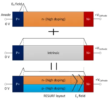
3.4. RESURF technologies ... 37
3.4.1.1-D model ... 38
3.4.2.2-D model ... 39
3.4.2.1 Bulk Si ... 42
3.4.2.2 SOI ... 45
3.5. On-resistance & Saturation current ... 48
Chapter 4
TCAD models verification and discussion ... 50
4.1. Introduction ... 50
4.2. TCAD software ... 50
4.3. Model benchmarking ... 51
4.3.1.The first benchmark structures (600 V) ... 53
4.3.1.1 Off-state characteristics ... 55
4.3.1.2 On-state characteristics ... 61
4.3.2.The second benchmark structure (~200 V) ... 62
4.3.3.Conclusion ... 64
Chapter 5
RESURF Si/SiC LDMOS designs and simulation setups... 66
5.1. Introduction ... 66
5.2. Si/SiC non-RESURF PiN diodes ... 66
5.2.1.Thermal simulation of the substrates ... 67
5.2.2.Electro-thermal modelling of PiN diodes ... 70
5.2.2.1 Simulated structures ... 70
5.2.2.2 Simulation setup ... 71
5.2.2.3 Simulation results ... 71
iv
5.3.1.600 V Si/SiC LDMOS with SOI RESURF ... 76
5.3.2.600 V Si/SiC LDMOS with PN RESURF ... 82
5.3.3.190 V Si/SiC LDMOS with SOI RESURF ... 85
5.4. Simulation setups ... 87
5.4.1.Application of the physical-based models ... 87
5.4.2.Simulated switching circuits ... 87
5.4.2.1 Clamped inductive switching (600 V) ... 88
5.4.2.2 Rectangular Power Pulse (600 V) ... 92
5.4.2.3 Capacitive load switching and Zener-diode-clamped inductive switching (190 V) ... 93
Chapter 6
TCAD study on the 600 V Si/SiC LDMOSFETs ... 97
6.1. Introduction ... 97
6.2. DC characteristics ... 97
6.2.1.Si/SiC LDMOS in SOI RESURF technology VS SOI ... 97
6.2.1.1 Off-state behaviour ... 98
6.2.1.2 On-state behaviour ... 99
6.2.2.Si/SiC LDMOS in PN RESURF technology VS Bulk Si ... 104
6.2.3.Temperature effects on the Si/SiC, SOI and Bulk Si LDMOS ... 105
6.3. Dynamic characteristics ... 110
6.3.1.Philips SOI vs Si/SiC on inductive switching ... 110
6.3.1.1 Overview of switching characteristics ... 111
6.3.1.2 Analysis of transient currents and power ... 113
6.3.2.Si/SiC, Philips SOI vs Bulk Si LDMOS on RPP circuit ... 119
6.3.2.1 Simulation results ... 119
Chapter 7
TCAD study on the 190 V Si/SiC LDMOSFETs ... 121
7.1. Introduction ... 121
7.2. DC characteristics ... 122
7.2.1.Off and on-state behaviour ... 122
7.3. Dynamic characteristics ... 123
7.3.1.Capacitive load switching ... 123
7.3.2.Zener-diode-clamped inductive switching ... 125
7.3.3.Conclusion ... 126
v
8.1. Conclusions ... 128
8.2. Future work ... 133
8.2.1.Experimental results ... 133
8.2.2.Physical-based TCAD models ... 133
8.2.3.RESURF design ... 134
8.2.4.Switching circuits ... 135
8.2.5.LIGBTs ... 136
Appendix… ... 137
A Thermal models ... 137
A.1 Methodology ... 137
A.2 Thermal conductivity and heat capacitance ... 138
B 3D RESURF for Si/SiC ... 141
C Experimental Si/SiC issues affecting TCAD simulation ... 144
C.1 The quality of Si on SiC ... 144
C.2 The (SI) SiC substrate ... 149
C.3 The Si/SiC interface ... 151
vi
List of figures
Figure 1.1. The basic features of the SOI (left) and the Si/SiC substrate (right) ... 3 Figure 2.1. Current applications of Si power electronics, taken from [18] ... 8 Figure 2.2. Current applications of Si power electronics, with the new frontiers enabled by SiC and GaN, taken from [18] ... 9 Figure 2.3. Two simple diagrams for a power diode (left) and a power MOSFET (right) ... 10 Figure 2.4. A simplified side view of a power module (left) and a 1-D thermal circuit consisting of multiple RC sections to represent the thermal properties of different materials (right). Thermal radiation and advection are not considered ... 12 Figure 2.5. Direct and indirect band structures for intrinsic semiconductors, with plus sign (+) and minus sign (-) indicating holes and electrons ... 17 Figure 2.6. The simplified bandgap structure of an intrinsic, P-type and N-type semiconductor ... 18 Figure 2.7. The band diagrams of a PN junction (left) and Metal-insulator-semiconductor (MIS) structure (right) ... 19 Figure 2.8. The simplified AlGaN/GaN HEMT structure and the band diagram at the gate region... 20 Figure 2.9. Intrinsic carrier density vs Temperature for different materials, namely Ge, Si, GaAs, InN, 6H-SiC, GaN and AlN [41] ... 21 Figure 2.10. The specific on-resistance vs breakdown voltage in [43] (left) and [44] (right), for vertical power MOSFETs made from Si, SiC and GaN ... 23 Figure 2.11. The specific on-resistance and breakdown voltage for LDMOSFETs at 25
⁰C (left) and 125 ⁰C (right), designed with different RESURF technologies [45] ... 23 Figure 3.1. I-V characteristics of a n-type LDMOSFET ... 31 Figure 3.2. A triangle relationship among BVDSS, Rsp and safe operation area (SOA) for
vii
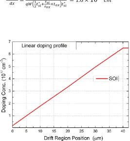
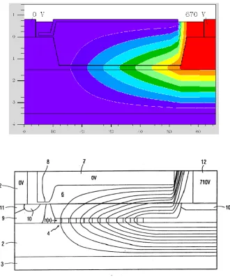
Figure 3.5. A simple demonstration of the RESURF concept by using three PiN diodes differing in the settings of the drift region ... 37 Figure 3.6. A reverse-biased PiN diode (left) and its corresponding electrical field distribution (right) ... 38 Figure 3.7. A HV LDMOSFET with stars indicating possible breakdown locations. AA’, BB’ and CC’ are the cutlines for analysing the E field along the surface, at the midpoint of drift region and under the N+ drain in vertical direction, respectively ... 40 Figure 3.8. The electric field distribution along AA’ (left) and BB’ (right), for the 1st order RESURF LDMOSFET ... 41 Figure 3.9. The electric field distribution along cutline AA’ (left) and BB’ (right), when the avalanche breakdown point is tend to be reached. ... 43 Figure 3.10. Double RESURF Layout (left) and the corresponding electric field along BB’ when the drift region is fully depleted (right) ... 44 Figure 3.11. Triple RESURF layout (left) and the corresponding electric field along BB’ when the drift region is fully depleted (right) ... 44 Figure 3.12. A 2-D SOI diode with the optimal RESURF condition under a reverse voltage of V, having an electric field Ex in x direction throughout a lateral depletion distance of about W (left), and a electric field distribution at location x highlighted in the device (right) ... 47 Figure 3.13. The relationship between the breakdown voltage and thicknesses of the Si and BOX layer in SOI devices, taken from [100] ... 48 Figure 3.14. A half bridge circuit consisting of a HV gate drive block, a low-side and high-side N channel LDMOSFET ... 49 Figure 4.1. One of the Philips SOI transistors [46] used in SILVACO for benchmarking, where the key parameters are indicated ... 53 Figure 4.2. The linear doping profile of the simulated SOI LDMOSFET ... 54 Figure 4.3. The potential contours of the benchmark LDMOS (top), and the Philips SOI (bottom) [121], on the verge of avalanche breakdown. (axes units: µm) ... 56 Figure 4.4. The potential and electric field at the middle of the N drift region, at the onset of avalanche breakdown ... 57 Figure 4.5. Off-state characteristics of the simulation SOI (Left) and the Philips SOI (right) [46], at room temperature and 200 ⁰C. The bottom graph from [110] is more similar to the simulation result ... 58 Figure 4.6. The temperature dependency of leakage current at VDS = 300 V for the
viii
Figure 4.8. The low-side resistance vs temperature for the simulated structure (left) and the Philips SOI (right) [46] ... 62 Figure 4.9. The second benchmark structure based upon [129], with a blocking voltage of 190 V ... 63 Figure 4.10. The off-state I-V curve (left) and potential distribution (right) at the onset of avalanche breakdown and 300 K, for the simulated structure (axes unit: μm) ... 64 Figure 4.11. The VGS-IDS curve at VDS = 0.1 V (left) and the on-state characteristics at
ix
Figure 5.15. 190 V LDMOSFETs using different substrates, namely Si/SiC, SOI, PSOSIC and PSOI ... 85 Figure 5.16. A flyback topology for AC/DC conversion [137] (left) and a half bridge circuit with an inductive load (right) ... 89 Figure 5.17. The lateral MOSFETs in the JI technology optimised for fully integrated AC/DC Power ICs [137] ... 89 Figure 5.18. A diode-clamped inductive switching circuit in the Mixed-Mode simulation ... 91 Figure 5.19. The rectangle power pulse circuit used in the Mixed-mode simulation for the 600 V LDMOSFETs ... 93 Figure 5.20. The simulated capacitive discharge circuit based upon [62], for the 190 V LDMOSFETs in Si/SiC, SOI, PSOI and PSOSiC technology ... 95 Figure 5.21. The clamped inductive switching setup with a Zener diode, for the 190 V LDMOSFETs ... 96 Figure 6.1. OFF-state I–V characteristics of the Philips SOI (left) and Si/SiC LDMOS (right)... 98 Figure 6.2. Off-state characteristics of the Si/SiC (black) and the SOI without the field plate extension (blue) ... 99 Figure 6.3. On-state characteristics of the Philips SOI (left) and Si/SiC LDMOSFETs (right), under isothermal conditions at 300 K ... 99 Figure 6.4. the ohmic regions of the I-V curves for the Philips SOI and Si/SiC at 300 K ... 100 Figure 6.5. The steady-state effect of self-heating on forward characteristics of SOI (left) and Si/SiC LDMOS (right), as well as their junction temperature (bottom) ... 101 Figure 6.6. Temperature contours of (left) SOI and (right) Si/SiC under VDS = 15 V, VGS
= 10 V conditions (axes units: μm) ... 102 Figure 6.7. On-state characteristics of the Si/SiC (black) and SOI without the field plate extension (blue), under isothermal conditions. ... 103 Figure 6.8. Off-state characteristics of the Si/SiC (dark blue) and the Bulk Si counterpart (green), at 300 and 573 K ... 104 Figure 6.9. On-state characteristics of the thick-film Si/SiC (left) and bulk Si LDMOSFETs (right), under isothermal conditions (300 K) ... 105 Figure 6.10. Temperature dependence of leakage current for the SOI, Bulk-Si, SOI Si/SiC and Bulk-Si Si/SiC LDMOS at a drain voltage of 300 V, along with two lines (∝ni &
x
thickness, namely 0.2 and 0.1 µm. The dotted line is derived from halving the curve for the SOI Si/SiC LDMOS with a 0.1-µm-thick Si film ... 107 Figure 6.12. Relationships between specific on-resistance and substrate bias for the simulated LDMOSFETs at 300 K and 573 K, excluding the one for the Bulk-Si at 573 K ... 109 Figure 6.13. Drain–source voltage and inductor current for the two transistors during VGS
= 10 V, 200 kHz switching nonisothermal simulations. The inductor and current-limiting resistor are 2 mH and 1800 Ω in Case 1 (Top) and 1 mH and 600 Ω in Case 2 (Bottom) ... 111 Figure 6.14. Dynamic temperature response of the two transistors in the nonisothermal switching for Case 1 (top) and Case 2 (bottom) ... 112 Figure 6.15. The current waveforms of the first switching cycle for the 600 V Philips SOI (top), 600 V Si/SiC (middle) and the 200 V SOI LDMOSFET in [152] (bottom) ... 114 Figure 6.16. The SOI and Si/SiC transient currents during the turn-on and off, in Case 1 ... 116 Figure 6.17. Power disspations calculated by ID × VDS and IG × VGS (top), and by IS×
VDS and ISUB× VDS (bottom) for the Philip SOI and Si/SiC in one cycle ... 117
Figure 6.18. The power pulses (top) and temperature responses (bottom) for the simulated 600 V structures ... 119 Figure 7.1. On (top) and off-state I-V curves (bottom) for the simulated 190 V devices under isothermal conditions at 300 K ... 122 Figure 7.2. The I-V switching behaviour during the turn-on for the four LDMOSFETs (top) and their drain and source currents (bottom)... 123 Figure 7.3. The instantaneous power and temperature responses during the capacitive discharge for the simulated LDMOSFETs ... 124 Figure 7.4. The Vds and Id curves under the conditions of Vpulse = 12 V, Vdd = 50 V, L =
5 mH, BVZener = 150 V, R1 = 3 kΩ and a ramp-up time of 10 µs, for the four simulated
xi
Figure C.1. Atomic force microscopy for the Si/SiC heterojunction layer by molecular beam epitaxy (MBE), designed to be 100 nm thick (left) and 1 µm thick (right) [38] . 145 Figure C.2. The 3 inch Si/SiC bonded samples before and after annealing (left & right). The Si seed wafer is treated with Smart CutTM process. ... 145 Figure C.3. SEM images of the Si/SiC samples in high angle (top), of top view (middle) and side view (bottom) ... 147 Figure C.4. (a) 100mm Si/SiC bonded wafers with a (1) 1-μm, (2) 2-μm or (3) 5-μm-thick Si film, as well as TEM views of the Si/SiC interfaces, showing (1) no interfacial layer, (2)&(3) presence of an amorphous layer and (4) an island-like defect, respectively [156] ... 148 Figure C.5. A cross-sectional view of a 4H-SiC lateral JFET on a (SI) SiC substrate, able to block voltage up to 3500 V [170] ... 150
List of tables
xii
Acknowledgements
I would like to first thank Peter Gammon, who has been supervising me and offering academic support throughout my PhD. You are a true professional, enthusiastic about research with an ambition to achieve the best, and more importantly always having an optimistic ‘aura’ around. No matter how negative I am to one question, you never show a sense of gloomy view but look on the bright side. Without this, I would have published fewer papers than I did, gotten stuck at one point and struggled to move forwards. Not to mention how many Chinglish you spot in my writing, all these let me know how to be competent, confident and self-motivated.
To my second supervisor Phil Mawby, I thank you for your enlightenment and encouragement for my first journal paper. Also the Chinese dinner you and your wife host each year is truly impressive, and I really appreciate your hospitality.
I would like to express my acknowledgements to my family, who have been supporting me during my PhD study. Without doubt, this contributes significantly to my work and continues to be one of important factors to push me forwards.
A special thank goes to Mark Crouch and Corinne Maltby, who are the technicians working at Science City cleanroom. Your experience, expertise and patience in teaching helped me gain some helpful skills about semiconductor processes. It is a priceless memory to be guided by someone with industrial backgrounds, and indeed will be quite useful in my upcoming career. I also appreciate the instructions on the MBE machine from one of our legends: Vishal Shah, though I never had a chance to operate it during my PhD.
xiii
xiv
Declaration
This thesis is submitted in partial fulfilment for the degree of Doctor of Philosophy under the regulations set out by the Graduate School at the University of Warwick. I certify that this thesis does not incorporate any material without acknowledgement previously submitted to any institution for a higher degree or previously published. The work is this thesis is my own except where stated, under the supervision of Dr Peter M. Gammon and Prof. Philip Mawby.
xv
List of publications
Patent
1. P. M. Gammon and C. W. Chan, (WO2016132089) Power Semiconductor Device, 2015. Filed, USA and UK, International Application No.: PCT/GB2015/050467. Link: https://patentscope.wipo.int/search/en/detail.jsf?docId=WO2016132089
Journal articles
1. C. W. Chan, F. Li, A. Sanchez, P. A. Mawby and P. M. Gammon, "Comparative Study of RESURF Si/SiC LDMOSFETs for High-Temperature Applications Using TCAD Modelling," in IEEE Transactions on Electron Devices, vol. 64, no. 9, pp. 3713-3718, Sept. 2017.
2. C. W. Chan, P. A. Mawby and P. M. Gammon, "Analysis of Linear-Doped Si/SiC Power LDMOSFETs Based on Device Simulation," in IEEE Transactions on Electron Devices, vol. 63, no. 6, pp. 2442-2448, June 2016.
Conference papers
1. C. W. Chan, F. Li, P. A. Mawby and P. M. Gammon, "Numerical study of energy capability of Si/SiC LDMOSFETs," 2016 European Conference on Silicon Carbide & Related Materials (ECSCRM), Halkidiki, Greece, Vol. 897, pp. 751-754, 2017.
2. C.W. Chan, Y. Bonyadi, P. A. Mawby, P. M. Gammon, "Si/SiC Substrates for the Implementation of Linear-Doped Power LDMOS Studied with Device Simulation", Materials Science Forum, Vol. 858, pp. 844-847, 2016.
xvi
Abstract
….
It is necessary for power laterally diffused MOSFETs (LDMOSFETs) to operate efficiently and reliably in high temperature (<300 ⁰C), hostile environments such as those found in downhole, space, automotive and aerospace applications. Currently, silicon-on-insulator (SOI) technology is a dominant method to achieve this goal due to low leakage current and complete electrical isolation. However, the buried oxide (BOX) layer causes self-heating, which can impact device performance, cause thermal runaway and shorten device lifetime. To address this issue, one solution is to combine a silicon thin film with a semi-insulating (SI) SiC substrate, forming the Si/SiC architecture. LDMOSFETs built on this substrate are expected to deliver much better thermal performance, with electrical isolation comparable to the SOI case. However, the Si/SiC LDMOSFETs do not have a strong substrate assisted depletion effect, which can result in poorer electrical performance than those of the Reduced Surface Field (RESURF) bulk-Si and SOI LDMOSFETs. This thesis investigates the PN and SOI RESURF layouts and uses them to optimise 190 V and 600 V Si/SiC LDMOSFETs. DC and transient modelling will be conducted on the optimised Si/SiC and their SOI and bulk-Si equivalents. Based upon this, several comparative studies are conducted on their simulation results to see the effects of the Si/SiC architecture on the LDMOS designs.
The comparative studies are made on the 600 V Si/SiC LDMOSFETs and their bulk Si and SOI equivalents. It is shown that the Si/SiC devices have the potential to operate with an off-state leakage current as low as the SOI device. However, the low-side resistance of the SOI LDMOSFET is smaller in value and less sensitive to temperature, outperforming both Si/SiC devices. Conversely, under high-side configurations, the Si/SiC transistors have resistances lower than that of the SOI at high substrate bias, and invariable with substrate potential up to −200 V, which behaves similar to the bulk-Si LDMOS at 300 K. A clamped-inductive switching circuit is simulated for the Philips SOI and the Si/SiC equivalent. It is shown that even though the SOI has a smaller chip area and suffered from strong substrate effects during the transient state, the two devices had similar currents and power dissipations at the gate, drain and source. The turn-on losses are higher than that of the turn-off losses due to the presence of parasitic capacitors. However, these similarities do not lead to similar thermal responses in both devices and the SOI is heated up at a much faster rate. By contrast, the SiC substrate in the Si/SiC behaves like an embedded heat sink regulating device temperature close to that of the ambient environment (423 K). In the high current condition, the peak temperature in the Si/SiC is 425 K, lower than 463 K in the SOI, thereby increasing reliability.
xvii
List of symbols and abbreviations
Ea Thermal Activation Energy
𝐶𝑃 Specific Heat at constant pressure
𝐸𝑔 Band Gap
𝑁𝐴 Acceptor Doping
𝑁𝐶 Effective Density Of States For Electron
𝑁𝑉 Effective Density Of States For Hole
𝑁𝑏 Base Doping
𝑄𝑒𝑓𝑓 Effective Dose
𝑇𝐿 Lattice Temperature
𝑉𝑑𝑒𝑝 Depletion Volume
𝑡𝑜𝑥 Oxide Thickness
𝑡𝑠𝑖∗ Effective Si Layer Thickness
𝜀𝑜𝑥 Oxide Dielectric Constant
𝜅|| Thermal Conductivity In Parallel To The C Axis
𝜅⊥ Thermal Conductivity In Normal To The C Axis
BVDSS Breakdown Voltage
EC Conduction Band
ECri Critical Electric Field
EF Fermi Level
ƐM Maximum Electric Field
Esurface Surface Electric Field
EV Valance Band
Ex Horizontal Electric Field
xviii
H Heat Generation
ℎ𝑐. 𝑎 Coefficient For Calculating Heat Capacitance
ℎ𝑐. 𝑏 Coefficient For Calculating Heat Capacitance
ℎ𝑐. 𝑐 Coefficient For Calculating Heat Capacitance
ℎ𝑐. 𝑑 Coefficient For Calculating Heat Capacitance
j Current Density
k Boltzmann Constant
L Device Length
Nd Doping Of The Drift Region
ni Intrinsic Carrier Density
Qd/q Drift Region Dose
RDS On Resistance
Rsp Specific On Resistance
T Temperature
Ta Ambient Temperature
Tj Junction Temperature
tsi Si Layer Thickness
U Recombination Rate
w
Lateral Depletion Distance Or Device Widthε
si Si Dielectric Constant𝐶 Heat Capacitance Per Unit Volume
𝑉 Voltage
q Elementary Charge
𝜇 Carrier Mobility
𝜌 Density Of The Material
xix
2DEG 2-D Electron Gas
2DHG 2-D Hole Gas
CDM Charge Device Model
BOX Buried Oxide
DI Dielectric Isolation
DRIE Deep Reactive Ion Etch
DUT Device Under Test
ESD Electrostatic Discharge
eSOA Electrical Safe Operation Area
FEM Finite Element Method
FET Field Effect Transistor / Field Emission Triode
FOX Field Oxide
GTO Gate Turn-Off
HBM Human Body Model
HCI Hot Carrier Injection
HEMT High Electron Mobility Transistor
HHMT High Hole Mobility Transistor
HTGB High Temperature Gate Bias
HTRB High Temperature Reverse Bias
HV High Voltage
IGBT Insulated Gate Bipolar Transistor
IOS Insulator On Silicon
JFET Junction Field Effect Transistor
JI Junction Isolation
xx
MIS Metal-Insulator-Semiconductor
MM Machine Model
MOSFET Metal–Oxide–Semiconductor Field-Effect Transistor
MTTF Mean Time To Failure
PCSS Photoconductive Semiconductor Switch
PSiP Power Supply In Package
PSoC Power Supply On Chip
PSOI Partial SOI
PSOSIC Partial Si/SiO2/SiC
RESURF Reduced Surface Field
RPP Rectangular Power Pulse
RTA Rapid Thermal Annealing
SEM Scanning Electron Microscopy
SI Semi-Insulating
Si/SiC Silicon On Silicon Carbide SiOSiC Silicon/Oxide/Silicon Carbide
SOA Safe Operation Area
SOD Si-On-Diamond
SODI Silicon On Double Insulator
SOI Silicon On Insulator
SON Silicon On Nothing
SOS Silicon-SiO2-Silicon / Silicon On Sapphire
SOTI Silicon On Thick Insulator
TCAD Technology Computer-Aided Design
TRIAC Bilateral Triode Thyristor
tSOA Thermal Safe Operation Area
xxi
1
Chapter 1
Introduction
Semiconductor devices are key elements in the development of compact, reliable and highly efficient power systems. Other than being used as passive components (e.g. resistors and capacitors), these fundamental devices can be deployed as switches that perform logic control or handle power flows, in the form of either diodes or transistors. Over past decades, the performance of power management modules has been improved significantly, due to the increase in system integration enabled by the advancement of semiconductor and packaging technologies. Examples of such integration are power supply in package (PSiP) and Power supply on chip (PSoC) [1], which feature smaller space, fewer components and reduced parasitic effect.
High voltage (HV) lateral transistors, for instance LDMOSFETs and LIGBTs, can be found in many integrated power systems, such as AC/DC power conversion, HV gate drivers and HV half-bridge stages [2]. Different from their vertical counterparts, their electrical contacts are on a single side of a semiconductor wafer, with the backside potential the same as that of an IC chip. Therefore, they can either be part of an IC chip where the CMOS components are made, or be a discrete unit sharing the same lead frame with the chip in a package [3]. Bulk-Si wafer is widely used for HV power devices, due to the cost-effectiveness of this substrate. The Silicon-on-insulator (SOI) solution is selected if high temperatures and a high degree of isolation is required. Self-heating may cause some problems in this structure, depending on the device area and pulse duration [4]. Considerable effort has been put into substrate engineering to achieve a better trade-off between electrical isolation and heat conduction, leading to structures like partial SOI (PSOI) [5], Silicon-on-sapphire (SOS) [6] and compound buried layers [7] [8].
2
survivability in the long term. Exposure to cosmic radiation, high temperature (200 ⁰C+) and high humidity can cause device malfunctions, which needs to be counteracted by a degree of protection. This could mean a larger area, more circuit elements and higher cost for an integrated system. In this respect, the implementation of SOD and Si/SiC in harsh environments seems more promising, as diamond and SiC are chemically inactive and highly thermal conductive, forming very reliable heat sinks. They are also free from a buried oxide (BOX) layer, which is one source of radiation-induced problems in the SOI layout.
Despite having higher heat transfer than SiC in theory, diamond used in practice is often synthesised and has electrical and thermal properties poorer than one in nature. High cost is one factor preventing diamond from being used in mass production currently, unless technological breakthroughs for this material emerge. Alternatively, semi-insulating (SI) SiC wafers are commercially available and has been employed in next generation electronics, such as AlGaN/GaN-on-(SI) SiC transistors at 500 ⁰C [9], 3510 V lateral SiC-on-(SI) SIC JFETs [10] and 50 kV (SI) SiC photoconductive switches [11]. It is worth noting that GaN and SiC-based devices can outperform their Si counterparts and revolutionise the integrated power systems. However, currently, SiC MOSFETs have a poor channel mobility, which prevents these devices being used in low voltage applications. In order to minimise the parasitic effects, GaN CMOS is being developed and was first reported in 2016 [12] as a stepping-stone for fully integrated GaN power systems. This can be a strong candidate in the harsh environment market, but requires a time period during which the associated technologies are developed, leading to the reduction of bulk/interfacial defects, cost and manufacturing difficulties. It takes time for the industry to manufacture these devices as well, for example, converting the conventional fabrication line to that suitable for such materials. As a result, the complete replacement of Si with wide band gap materials for electronics is a long-term process and more likely, both will co-exist and complement each other in some applications.
3
This nature determines that the Si/SiC devices are still bound by the Si limits, such as the critical breakdown field and maximum junction temperature (300 ˚C). However, this also indicates that these devices can be produced with the traditional Si technologies and manufacturing foundry, with the SiC being the only new aspect. Wafer bonding, which binds materials with atomic bonds, can treat this new aspect as a purely SOI case and minimise the problems encountered in the hetero-epitaxy growth [13]. In addition, it has been proven experimentally [14, 15] that the Si fabrication processes can engineer the Si layer of the Si/SiC structure, resulting in electrical characteristics similar to those extracted from the equivalent bulk-Si and SOI devices.
Figure 1.1. The basic features of the SOI (left) and the Si/SiC substrate (right)
1.1.
Background
This thesis summarises the initial development of Si/SiC power LDMOSFETs which comprises the theoretical study of the RESURF technologies, TCAD models verification and discussion, design of RESURF Si/SiC LDMOSFETs and numerical analysis of the Si/SiC LDMOSFETs by TCAD simulation. The effect of such architecture on the electrical and thermal characteristics was reported and evaluated, by using bulk-Si and SOI devices as references for comparison.
4
was that the top Si film could be fully oxidised to form a SiO2 layer on top of SiC.
Alternatively, it was proposed as a low-resistance ohmic contact to p-type SiC [13]. Both have the potential to significantly improve the SiC-based devices, yet with some difficulties being introduced, such as the precise control of the thermal oxidation and the reduction of carrier scattering at the Si/SiC hetero-junction [13]. No subsequent work has been carried out to address these issues and therefore, this architecture has not been implemented for SiC products so far. Nevertheless, it is the success in establishing Si/SiC substrates with wafer bonding, as demonstrated in those studies [13, 16] that laid a foundation for the this project, where the Si/SiC hetero-structure is designed to behave like SOI with better thermal conductivity, thereby minimising self-heating effect.
This Si/SiC concept was not without problems. One concern was the presence of disordered layers at the bonded Si/SiC interface, which can negatively affect the device performance. Secondly is whether the SiC can be treated as a dielectric material, by which the active region is confined and leakage current reduced. These were not answered until Shinohara et al. demonstrated experimentally the first functional Si/SiC MOSFETs, with the electrical characteristics comparable to a bulk-Si equivalent [14]. Soon after this, Lotfi et al. showed that even the poly-SiC was capable of offering decent electrical isolation, and that the resulting Si/SiC LDMOSFET performed in a way similar to their fabricated SOI devices [15]. Supported by this evidence, the Si/SiC structure appeared suitable for use in Si-based lateral power electronics.
5
1.2.
Thesis outlines
The following chapter first introduces the applications of power electronics and the challenges of harsh environment operation. Next, the high temperature effects on the semiconductor devices are presented before moving on to the approaches to manage the junction temperature and the stress tests to qualify the device’s reliability at high temperature. Following this, the high temperature potential of different semiconductors are discussed based on their physical properties and technologies. Finally, two solutions to high temperature operation are discussed, namely semi-insulator and vacuum electronics. This chapter is aimed to offer a general view of how competitive Si-based RESURF LDMOSFETs are to be used for high temperature power ICs (<300 ⁰C), compared with power switches made from wide/ultra-wide bandgap materials. This device type will be incorporated into the Si/SiC architecture in the following chapters.
Chapter 3 presents some background knowledge required to understand the results chapters. The first to be introduced is the LDMOSFET I-V behaviour, followed by an introduction of different substrates for the LDMOSFET. After this, the LDMOS structure will be described prior to the investigation on the SOI and PN RESURF technologies. The last section talks about the on-state resistance and saturation current of the LDMOS, in terms of low and high-side configuration as well as their temperature dependencies.
In Chapter 4, a 600 V and a 190 V SOI LDMOSFET were constructed in the simulator to verify the TCAD models against the references over the temperature range of 27-300
⁰C. In Appendix C, the transferability of these models to the Si/SiC architecture are discussed with the literature. These two procedures are aimed to ensure the credibility of the simulation results.
6
setups are detailed, with emphasis on the four switching circuits for the aforementioned LDMOSFETs. They are a clamped-inductive circuit, a rectangular power pulse circuit, a capacitive and an inductive circuit with a Zener diode. The first two are for the 600 V devices and the other two for the 190 V transistors.
Chapter 6 provides a TCAD study on the static and dynamic characteristics of the 600 V Si/SiC LDMOSFETs. The DC analysis first compares the Si/SiC device in the SOI RESURF technology with its SOI equivalents. Secondly, the Si/SiC LDMOSFET in the PN RESURF technology is compared with its bulk-Si counterpart. The last part compares all the aforementioned 600 V transistors, in terms of the leakage current, low and high-side resistance. The study on the transient characteristics are split into two parts and based upon the switching circuits described in Chapter 5. The first section compares the dynamic behaviour of the Philips SOI and its Si/SiC equivalent in the inductive switching circuit mentioned in Chapter 5. Next, comparison is made among the Philips SOI, bulk Si and the two Si/SiC LDMOSFETs, of the heating effects in the RPP circuit introduced in Chapter 5.
Chapter 7 presents a TCAD study on the energy capability of 190 V LDMOSFETs in Si/SiC, SOI, PSOI and PSOSiC technology, using the capacitive and inductive switching circuit mentioned in Chapter 5. The first section of this chapter analyses the on/off I-V behaviour of the four transistors under isothermal condition at 300 K (27 ⁰C). Secondly, a comparison is made between the four transistors on their switching performances during the capacitive turn-on and inductive turn-off events.
7
Chapter 2
High temperature
power electronics
2.1.
Introduction of power electronics
Semiconductor devices have already penetrated every single aspect of human life, from food production, trading and transportation, to education, entertainment and medical treatment. All these activities depend on power generation and distribution systems, which employ a large number of electronics as well. Power electronics is a term to describe semiconductor devices that control or convert electrical power, instead of sensing or processing signals and data.
With the advance of semiconductor technologies, many forms of Si power electronics have been invented for a specific function, to achieve a better compromise between cost, efficiency, complexity and robustness. As can be seen in Fig. 2.1, the capacity (VA) and operation frequency (Hz) is one trade-off that determines the selection of different Si power electronics. The thyristor family, namely Gate turn-off (GTO), bilateral triode thyristor (TRIAC) and normal thyristors, are capable of handling very high power, but perform poorly in medium-to-high frequency operations. Insulated gate bipolar transistors (IGBTs) exhibit a better switching behaviour than thyristors, at the expense of a lower power handling ability. Metal–oxide–semiconductor field-effect transistor (MOSFETs) modules are better options than IGBTs for applications where high frequencies are involved, though the capacity level is reduced even further. High voltage and power integrated circuits (HVICs & PICs) are compact solutions specific for very high frequency operations, albeit its power capability is the least among the power electronics illustrated in Fig. 2.1.
8
Figure 2.1. Current applications of Si power electronics, taken from [18]
9
Figure 2.2. Current applications of Si power electronics, with the new frontiers enabled by SiC and GaN, taken from [18]
10
Figure 2.3. Two simple diagrams for a power diode (left) and a power MOSFET (right)
2.2.
Harsh environment operations
One challenge in power electronics is the exposure to harsh environment which includes but not limited to shock, high vibration, high radiation and high/low temperature. These extreme conditions can occur simultaneously or/and successively, depending on different applications. In automotive and aerospace, there is an increasing demand in the replacement of traditional mechanical, hydraulic and pneumatic units with electronics for higher reliability and lower life-cycle cost [19, 20]. In this case, semiconductor components will be placed close to the engine and experience vibration and high temperature (125~150 ⁰C) [20]. Electronics solutions in well-logging will suffer even more severe conditions, for example shock, extreme vibration and very high temperature (225 ⁰C), which surpass some military specifications [21]. Nuclear plant and waste storage is one area in need of radiation-hard power electronics, for achieving more reliable fuel usage and recycling [22].
11
2.2.1.
High temperature environment
Among all the extreme ambient conditions, high temperature is of paramount importance in power electronics as it appears in most harsh-environment applications and can induce various side effects, such as chemical reactions, dopant diffusion, performance degradation, electromigration and mechanical stress [22]. Some of these phenomena can cause irreversible damage to semiconductor devices, resulting in system breakdown and a short lifetime. Additionally, the solutions to these failure mechanisms can increase complexity and cost, perhaps with some parameters being compromised. One typical example is the mean time to failure (MTTF) due to electromigration, described by Black’s equation (see below) [22]:
𝑀𝑇𝑇𝐹 = 𝐴𝑗−𝑛𝑒𝐸𝑎⁄𝑘𝑇 (2.1) Where A is a metal process specific coefficient, j is current density, n is a factor (typically 2 or 3 [22]) T is temperature and Ea is a thermal activation energy. It can be
found in Equation 2.1 that MTTF is less sensitive to current density (j), than Ea and T
which form the exponent with the Boltzmann constant (k). Even so, it is much easier to reduce the current density for a longer lifetime as this can be done by just adjusting the bias conditions, whereas the variation of Ea involves the change of recipe for contact
metals [20, 22] and the reduction of temperature depends on the design of cooling equipment which is more challenging in a hot environment.
2.2.2.
Self-heating effects
It should be noted that the temperature in equation 2.1 is not always equal to ambient temperature. The device will generate power losses in operation, which will mean the local junction temperature (Tj) is greater than the ambient temperature (Ta) by an amount
dependent on the thermal properties of the system. This will contribute to a decrease of the MTTF according to Equation 2.1, while a variation of Tj within a device can also exist,
12
One way to regulate temperatures of a power module is to improve heat transfer by using techniques such as air flow cooling, liquid cooling, microchannel cooling, and electrical-thermal cooling [26]. Common to those methods is the presence of a heat exchanger, which can be a heat sink, liquid-cooled cold plate or P/N type pellets [26]. A heat sink is made from metals with good thermal conductivity (e.g. Al & Cu), and can achieve enhanced heat conduction with fins and flip-chip layout [26]. The implementation of liquid-cooled cold plates and circulation of fluid flows in a package can lead to thermal convection, thereby reducing heating effects. By biasing P/N type pellets, the heat can be pumped from the device and directed to an external heat sink, yet with poor thermal efficiency [27].
Figure 2.4. A simplified side view of a power module (left) and a 1-D thermal circuit consisting of multiple RC sections to represent the thermal properties of different
materials (right). Thermal radiation and advection are not considered
Fig. 2.4 depicts a simple layout for a power component where a heat sink is used for heat extraction from a die. Between the die and heat sink are a copper lead frame and thermal interface materials for adhesion. Also illustrated is a Cauer thermal network formed by a series of RC sections, each of which represents the unique thermal properties of different substances along the vertical heat transfer path. In this circuit, a source is employed to simplify the power dissipation of a device, and thermal radiation and convection are not taken into account. If the source outputs a DC power signal, all the thermal capacitors are open-circuited and the junction temperature can be obtained by Equation 2.2:
13
also be cooled down by lateral heat transfer and thermal radiation, neither of which are considered in the 1-D Cauer network. On the other hand, the switching mode will lead to dynamic losses, which can be significant if a device is driving inductive loads or working at high frequencies. Complicating matters further, thermal impedance is not constant and increases with increasing temperature. When all these issues are factored in, Equation 2.2 appears to be unreliable and a much more detailed model of junction temperature must be derived from finite element methods (FEM).
Another approach to avoid overheating is the application of sensors in a device. This enables the power electronics to be ‘self-aware’ of the danger that can happen, and respond to it by entering the off-mode. For instance, once the voltage, current or temperature exceed the maximum allowable value, the sensing units will take over the gate control of a transistor and shut it down forcibly [28]. During this idle state, power dissipation significantly drops and temperature is reduced to a safety level, after which device functionality is restored. For achieving an uninterrupted operation, it is necessary to add some redundancies into the system, such as a backup unit that delivers the same function as the device under thermal cut-off. Such protection will make the power module more reliable, but features a complex logic that gives rise to cost and longer development time.
2.2.3.
High junction temperature operation
14
2.2.4.
High temperature reliability tests
Before being launched onto the market, semiconductor products will undergo a series of tests to define their lifetime, safe operation area, degradation and fail mechanisms. The tests often stress the products with high humidity, high temperature and high voltage, which makes them degenerate at a fast rate and eventually leads to device breakdown [31]. These tests can not only show the reliability and robustness of devices working in harsh environments but also indicate the period over which the electronics will operate under normal conditions prior to malfunctioning. There are many stressing tests for different applications [32] [31], among which high temperature reverse bias (HTRB) test, high temperature gate bias (HTGB) test and electrostatic discharge (ESD) test are essential to power transistors designed to work at high temperature.
In the HTRB tests, a power IGBT/MOSFET will be configured in a static mode at 150
15
2.3.
Semiconductor materials and technologies
16
2H
-AlN 6.2 D ~10
-34
8.5 300 12 1.7 2.85
Ta ble 2 .1 P hysi ca l prope rtie
s of se
mi
conduc
tor m
ater
ials a
t 300 K
[22 ] [36 ] [37] Dia mond 5.45 I 1.6 × 10 -27
5.5 2800 10 2.7 22
Ga 2 O3 4.5 -4.9 D 2.6 × 10 -19 -1.2 × 10 -22
10 300 8 —
0.13 -0.21 4H -S iC 3.26 I 8.2 × 10 -9
10 900 3 2.0 4.5
2H -Ga N 3.39 D 1.9 × 10 -10 9.9 900
-2000 3.5 2.5
1.3 [38] AlGa As (a ll oy)
1.9 D — — 3000 0.5 1.0 0.1
Ga As 1.42 D 1.8 × 10 6
13.1 8500 0.4 1.2 0.55
Si 1.12 I
1.5
×
10
10
11.8 1350 0.25 1.0 1.5
Ma ter ial Eg ( ev) Dire ct/ Indir ec t ni (c m -3 ) εr μn (c m 2 /V·s) Ec (MV /cm) Vsat (10
7 c
17
Table 2.1 lists several material parameters associated with power devices, for Si, GaAs and AlGaAs, wide band-gap 2H-GaN and 4H-SiC as well as ultra-wide band-gap Ga2O3,
Diamond and 2H-AlN [36]. Every semiconductor has its unique band structure, which is responsible for their distinct characteristics. The differences in the band structure can be simply described by the band gap and whether the band is direct or indirect. As shown in Fig. 2.5 for an intrinsic semiconductor, the band gap is defined as the difference between the minimal energy state of the conduction band (EC) and the maximal energy state of the
valance band (EV). If these two states occur at the same momentum, the band structure is
direct, otherwise it is indirect (see Table 2.1). The band gap indicates the minimum energy required by an electron to move from the valance band, which is almost filled by electrons, to the conduction band, which is nearly empty. In the valance band, voids are created after the electron displacement and are termed holes. The generated electron-hole pairs will increase the conductivity of an intrinsic semiconductor, with the few electrons freely traveling in the conduction band, and the holes representing the massive movement of electrons in the valence band. Within the bandgap of an intrinsic semiconductor, there are no other electron states that contributes to the current conduction. The higher the lattice temperature is, the more electron-hole pairs that will be produced, as greater thermal energy is available for the electron transition. However, a wider bandgap leads to a lower intrinsic carrier density (ni) (see Table 2.1), thereby reducing the off-state current
and enabling high temperature applications.
18
It can also be found in Table 2.1 that a wider bandgap gives rise to a higher critical electric field (ECri). The critical electric field is the limit beyond which the semiconductor
loses its intrinsic property and becomes a low resistance short, the result of avalanche breakdown [39]. Avalanche occurs when highly energised carriers collide with the lattice freeing more electrons which are then also energised, producing electron-hole pairs. However, the electrons cannot be set free from the lattice if the energy they possess is less than that of the bandgap. This is similar to the previous case where the electron-hole pairs are thermally produced, albeit the cause here is the electric potential energy.
Within a bandgap, the position of the Fermi level (EF) with respect to the band edges
(EC or Ev) determines the electrical conductivity of a material. In an intrinsic
semiconductor, the Fermi level is close to neither EC nor Ev, resulting in the least amount
of carriers for current conduction (see Fig. 2.6). By introducing dopants in the intrinsic semiconductor, the Fermi level will be shifted towards EC or Ev according to the dopant
type and density. Assuming that all the dopants are ionised, the Fermi level near EV
induces a great number of holes with very few electrons. This extrinsic semiconductor is referred to as P-type material with holes as majority carriers. The opposite case is N-type materials whose majority carriers are electrons.
Figure 2.6. The simplified bandgap structure of an intrinsic, P-type and N-type semiconductor
19
(ƐM) which is proportional to the square roots of applied voltage and doping concentration
[39]. This means that if the PN junction is reverse-biased and doping level is high, the ƐM
can reach the avalanche breakdown limit of a material with a relatively low applied voltage. This relationship is of paramount importance in the design of power electronics. Another way to alter an extrinsic material is by using a metal-insulator-semiconductor (MIS) structure (see Fig. 2.7 right). By applying a positive voltage at the gate, the surface area of the semiconductor will be depleted and exhibit intrinsic property. However, if the bias is large enough, the Fermi level will approach EC and an inversion layer formed,
which is responsible for the current conduction in n-channel enhancement mode MOSFETs [39].
Figure 2.7. The band diagrams of a PN junction (left) and Metal-insulator-semiconductor (MIS) structure (right)
In High Electron Mobility Transistors (HEMTs), the electrical conductivity depends more on the surface band bending than the doping level. This is explained in Fig. 2.8 where a band diagram of AlGaN/GaN heterojunction is illustrated. The bandgap of GaN is smaller than that of AlGaN. Due to the discontinuity in the polarisation field at the junction [37], positive interfacial charges are generated and pull the band downwards at both sides. In this case, the Fermi level is above EC near the junction in the GaN, which
20
thereby minimising the effect of impurity scattering on mobility [37]. GaAs is another III-V group material for HEMTs, albeit no polarisation effect is involved. This mechanism can also be implemented in the Al2O3/Diamond heterojunctions with the
C-H surface treatment, though the conduction relies on holes and the resulting devices are termed High Hole Mobility Transistors (HHMTs) [40].
Figure 2.8. The simplified AlGaN/GaN HEMT structure and the band diagram at the gate region
2.3.1.
Semiconductors of choice for high-temperature power
applications
At sufficiently high temperature, the intrinsic carrier density (ni) will dominate the
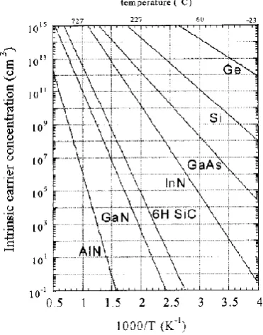
electrical properties of semiconductors, instead of the manufacturing processes performed on them. When this occurs, the device is non-functional as there is little difference between the on and off-state current. Therefore, the intrinsic carrier density can be used to predict the maximum operating temperature for a semiconductor. Fig. 2.9 shows the relationship between the ni and temperature for different materials [41]. Ge and InN are
not relevant here. Although 4H-SiC, Ga2O3 and Diamond are not shown in the plot, the
21
[image:43.595.226.412.269.506.2]power systems made from wide/ultra-wide-bandgap materials, due to the lack of packaging and cabling able to work reliably beyond 300 ⁰C [22]. Therefore, 300 ⁰C is the upper limit of the ‘high temperature’ described in this work. In the range of 27-300 ⁰C, other factors can be as important as temperature for the leakage current in wide/ultra-wide-bandgap materials. For example, Lee et al. found that at room temperature, the leakage of their HV SiC LDMOSFETs was measured to be a value three order of magnitude higher than that obtained from the simulation [42]. This is because the modelling only considered the effect of intrinsic carrier density on the leakage but in reality, material defects can dominate the off-state characteristics [42].
Figure 2.9. Intrinsic carrier density vs Temperature for different materials, namely Ge, Si, GaAs, InN, 6H-SiC, GaN and AlN [41]
2.3.1.1
Silicon
Si is the most widely-used and commercialised material in the semiconductor industries due to its low cost, very high integration level and processing maturity [22]. In spite of having a mediocre thermal conductivity, the smallest bandgap and critical field in Table 2.1, Si is still a strong candidate for power electronics if the targeted voltage and temperature are less than 1200 V and 300 ⁰C. Furthermore, the native oxide layer (SiO2)
22
23
Figure 2.10. The specific on-resistance vs breakdown voltage in [43] (left) and [44] (right), for vertical power MOSFETs made from Si, SiC and GaN
Figure 2.11. The specific on-resistance and breakdown voltage for LDMOSFETs at 25 ⁰C (left) and 125 ⁰C (right), designed with different RESURF technologies [45]
2.3.1.2
GaAs
24
to about 0.15 Wcm-1K-1 at 573 K [47], which makes heat extraction more difficult than the Si in elevated temperature operation.
2.3.1.3
GaN
GaN is very similar to GaAs in some aspects, for example the fabrication steps and device layout (HEMTs). However, this semiconductor has a much wider bandgap and higher thermal conductivity, which are favourable to high temperature power applications. In addition, this material can be grown on (SI) SiC substrates for enhanced thermal performance [9], but a much higher cost will be incurred. Theoretical speaking, GaN is more advantageous than Si and SiC for HV power transistors, regardless of the implementation of RESURF concept (see Fig. 2.10 right) [44]. However, the research to approach the GaN limit is in progress and more investigations need to be done to ascertain the surface, bulk quality and defect density of this material [36]. Recently, functional GaN CMOS devices have been demonstrated, which lays a foundation for the GaN power ICs [12]. However, the electron mobility (300 cm2V-1S-1) was found to be much lower than that of the discrete GaN transistors (1000 cm2V-1S-1), and the hole mobility is only 20 cm2V-1S-1 [12]. To sum up, more research needs to be done to achieve the full potential of GaN in power transistors.
2.3.1.4
SiC
25
voltage up to 3000 V [52] [42]. It can be seen that none of the state-of-art SiC devices aforementioned is designed for low-medium (≤ 600 V) power applications. This is because SiC MOS channel has a very poor mobility, which substantially raises the on-resistance if the rated voltage is not very high. As can be seen in Fig. 2.10 left, the theoretical SiC limit is only able to correctly describe the practical devices above 4000 V, with a substantial deviation below 1000 V. Furthermore, there are many traps at the SiO2/SiC interface and its quality has not yet matched the SiO2/Si in the Si MOS channel
[36].
2.3.1.5
Ga
2O
3β-Ga2O3 is found to be the most stable form of this compound material for device
fabrication and has a bandgap wider than those of GaN and SiC [36]. The availability of melt-growth techniques for this semiconductor enables large volume and low cost production, which is similar to the Si case [36]. It has been experimentally shown that to block 230 V, the Ga2O3 MOSFETs require a gate-to-drain spacing of only 0.6 µm,
meaning that the average and breakdown field are up to 3 and 5.8 MV/cm respectively [36]. Wong et al. reported a 750 V Ga2O3 MOSFET, built into a (UID) Ga2O3 buffer layer
on a (SI) Ga2O3 substrate [53]. This layout provides a very good electrical isolation at
high temperature and stable performance is observed up to 300 ⁰C, without irreversible thermal damage [53]. Nonetheless, Ga2O3 is a very powerful thermal insulator (0.13-0.21
W/cmK) and the electrical isolation achieved by this material alone will worsen the self-heating effect. To address this problem, (SI) 4H-SiC can be used as a platform for cooling the Ga2O3 transistors, as proposed by Russell et al. [54]. Another issue facing Ga2O3 is
the lack of p-type dopants. As a consequence, the reported Ga2O3 transistors are all
depletion-mode N-channel devices and normally-on at zero gate-source voltage [36]. Furthermore, p-type conduction can be hindered by self-trapping of holes in the bulk Ga2O3, as predicted in [36] [55].
2.3.1.6
Diamond
26
to GaAs and GaN [36]. Diamond devices in both technologies exhibit very high breakdown fields in the range of 2 to 10 MV/cm, and high blocking voltages up to 2000 V [36]. It is shown that at room temperature, the diamond HEMTs have a leakage current 2-3 orders of magnitude lower than those of AlGaN/GaN HEMTs [40]. With the improved deposition process for the Al2O3 cap layer, the sheet resistivity and hole density
of 2DHG were found to be almost constant at temperatures between 27 to 500 ⁰C, which is more desirable than boron-doped diamond FET for high temperature applications [56]. The formation of a partial C-O channel enables normally-off behaviour in the diamond HEMTs, a valuable feature for safe operation [40]. However, the absence of effective n-type dopants restricts the device n-types that can be made from this material [36].
2.3.1.7
AlN
AlN is a very good thermal conductor with a bandgap even wider than that of diamond. Therefore, this material can be used as a heat sink with a remarkable insulating property. Research on this nitride for HV electronics is still at early stage but the preliminary results by Fu et al. are encouraging [57]. Their lateral 1 kV Schottky diode has an n-type AlN layer as the active region, on an unintentional doped (UID) AlN for electrical isolation [57]. The breakdown mechanism is believed to be associated with the electric field crowding at the edge of Schottky contact, rather than the AlN layers [57]. A noticeable rectifying I-V relationship is demonstrated at room temperature, featuring a turn-on voltage of 1.2 V, an on/off current ratio of 105 and a reverse current below 1 nA [57]. All these indicate the potential of AlN to be used for high temperature and power IC applications.
2.3.2.
Conclusions
27
2.4.
Others technologies for high-temperature devices
Having introduced different semiconductors and their technologies, presented here are another two solutions that can realise high-temperature power electronics, namely semi-insulator and vacuum technologies.
2.4.1.
Semi-insulator technologies
Semi-insulating (SI) semiconductors are gaining interest for use in the harsh environment, specifically given recent interest in photoconductive semiconductor switches (PCSS). SI semiconductors no longer rely on foreign elements to increase its electrical conductivity. Instead, in order to raise the resistivity of the material, it will either remain unintentionally doped, or will be electrically neutralised by implanting deep-level dopants. This intrinsic behaviour can be disrupted by exposing the material to laser pulses, which deliver significant optical energy. This allows the SI semiconductor to be populated with carriers, resulting in current conduction. This phenomenon is similar to the effect of temperature and electric field on the electron-hole pairs aforementioned, however this laser excitement is deliberate and controllable. The more laser energy the semiconductor absorbs, the lower the on-state resistivity will be. Devices exploiting this optical mechanism are termed photoconductive semiconductor switches (PCSS). Such devices can demonstrate a very high on/off ratio and its electric field distribution can be quite even, thereby increasing the breakdown voltage. Furthermore, the semiconductor is not heavily engineered—only metal contacts are compulsory—which can avoid the damage introduced during the fabrication in semiconductor technologies.
28
measured to be 27 MW and 50 kA/cm2, respectively [11]. Even though no results have been reported on their high temperature operation, it can be expected that devices of this kind resemble the SiC-based electronics in semiconductor technologies to some degree, in terms of the electrical characteristics in hot environment. More specifically, in the off-state where the optical source is turned off, the SiC PCSS can be regarded purely as a semiconductor device and the leakage will go up with increasing temperature like its traditional counterpart. In the on-state, the resistance is related to the device geometry and inversely proportional to the carrier mobility and density [11]. Therefore, the two device types share the same principle for current conduction, which can lead to a similar temperature dependency in the on-state if the optical carrier generation in the PCSS is not strongly sensitive to temperature. One can infer that carrier lifetime is one reason for the temperature sensitivity of the optical process but this is not formulated in the equations in [11], where the process is demonstrated to be temperature-independent.
2.4.2.
Vacuum technologies
After being usurped by semiconductor devices and replaced in the majority of applications, vacuum electronics were not completely eliminated and are still used in a few areas. One example is the traveling-wave-tube amplifier used for satellite communication [60]. Over more than half a century, there has not been a semiconductor device that can challenge its position [60]. High temperature operation is another field where an intense competition between vacuum and semiconductor technologies can happen. Even though both device types suffer thermal degradation caused by chemical reaction, metal diffusion and packaging [22], the carrier transport in vacuum electronics is temperature-independent [22], which is different from the semiconductor counterparts. It has been demonstrated that miniature thermionic vacuum circuits can work with little or no loss of functionality in 13000 h test at 500 ⁰C [22].
29
30
Chapter 3
Theory
In this Chapter, the principle of LDMOSFET and its figure-of-merits are first stated to offer background information for this work. Prior to the discussion of RESURF technologies, different types of substrates are introduced and compared, with their pros and cons detailed. The last section briefly talks about the on-state resistance and saturation current of the LDMOS, in terms of low and high-side configuration as well as their temperature dependencies.
3.1.
Introduction of LDMOSFET
By convention, LDMOSFET is a unipolar device whose on-state current conduction relies on only one type of charge carrier, namely electrons or holes. The LDMOSFETs that employ these two carriers are termed nLDMOS and pLDMOS, respectively. They have the same operation but differ in the polarity of the doped regions and bias conditions for the terminals. Unless stated otherwise, the LDMOSFET described in this section is n-channel, with electrons constituting the main current flow.
Similar to a MOSFET, the operating modes of a LDMOSFET are determined by the voltages applied to its four electrodes, namely source, drain, gate and substrate. Normally speaking, the substrate is connected to ground and its potential can be equal to or lower than that of the source. To turn on the device, the gate-to-source potential (VGS) has to
exceed the threshold voltage (Vth), with the drain more positively biased than the source.
In this case, the transistor will be operated either in the linear region if the drain-to-source voltage (VDS) is small, or in the saturation region if VDS is large (see Fig. 3.1). The
drain-to-source current (IDS) is increased with higher VDS and VGS in the linear region, whereas
in the saturation region it is only a function of VGS. If self-heating effects are considered,
the saturation current will be reduced and negative resistance occurs (see the dashed lines in Fig. 3.1). This is due to the increased power dissipation as VDS goes up, raising the
temperature and therefore lowering the carrier mobility.
With VGS equal to zero, the device is in the off-state mode and only shows considerable
31
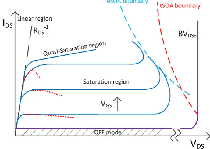
Increasing VGS leads to a reduction in BVDSS because the number of mobile charges is
increased, which causes high electric field at the drain side [62]. This is called the Kirk effect and the resulting avalanche process will generate holes which drift to the source [63, 64]. If this hole current is large enough, the parasitic npn transistor will be triggered and the LDMOSFET loses control [63, 64]. This forward breakdown voltage at each VGS
[image:53.595.151.496.359.603.2]outlines the boundary of the electrical safe operation area (eSOA). Likewise, the thermal safe operation area (tSOA) defines the conditions under which the transistor starts to show thermal instability. The parasitic npn structure also plays an important role in this case but the device malfunction is initiated by junction temperature [64]. In practice, the safe zone of a device will be influenced by combined electro-thermal actions and changes with bias conditions and ambient environment. At high temperature, increasing the device area and choosing high thermally conductive materials can effectively enlarge the SOA, as the faulty operation is more easily activated by the thermal effects than the electrical.
Figure 3.1. I-V characteristics of a n-type LDMOSFET
The high BVDSS is one aspect that differentiates LDMOSFETs from its low-voltage
counterparts. This is enabled by introducing a lightly-doped (drift) region between the gate (channel) and drain contact region. This voltage-sustaining region reduces the sensitivity of current to the gate bias at high VGS, creating a quasi-saturation region (see
32
screening [66]. The drift region also requires a larger chip area (A) and will increase the on resistance (RDS). The product of RDS and A is termed specific on resistance (Rsp), and
widely used to benchmark the on-state performance of various LDMOSFETs. Rsp and
BVDSS are a pair of trade-off factors and have been studied for many years, which
eventually led to the Reduced Surface Field (RESURF) principle, which will be discussed in depth later. Using this concept, a better compromise between BVDSS and Rsp can be
realised in a power transistor, which translates into a smaller chip area and lower cost. In practice, the device area can be larger than that determined by the RESURF principle so that a better ruggedness and energy capability can be achieved in the LDMOSFET [63]. Therefore, the final product is more likely to be conceived by seeking the balance among BVDSS, Rsp and safe operation area (SOA) (see Fig. 3.2 [64])
Figure 3.2. A triangle relationship among BVDSS, Rsp and safe operation area (SOA)
for LDMOS design, taken from [64]
![Figure 2.1. Current applications of Si power electronics, taken from [18]](https://thumb-us.123doks.com/thumbv2/123dok_us/9433784.449868/30.595.138.507.80.346/figure-current-applications-si-power-electronics-taken.webp)
![Figure 4.1. One of the Philips SOI transistors [46] used in SILVACO for](https://thumb-us.123doks.com/thumbv2/123dok_us/9433784.449868/75.595.175.472.128.329/figure-philips-soi-transistors-used-silvaco.webp)