Abstract—In this paper, we implement a circuit topology for the gold standard ATX80+.The total output power is 255 watts under full load operation. An active-clamping ZVS forward converter is adopted to provide main power and in secondary side, the BUCK circuit technology is adopted to provide 3 sets power +12V, +5V and +3.3V. To eliminate the current harmonics and to achieve high power factor, an active power factor corrector is added to the implemented power supply. And a two-step follower boost circuit is used to decrease PFCs output voltage which will reduce power losses of the switching loss and conduction loss during loads of light load and typical load. During high load, in active clamp circuit, output diode will be converted into MOSFET, and a current transformer both are used to reduce total power consumption in order to comfort the EPA regulation.
Index Terms—active clamp, forward converter, quasi resonant, boost PFC
I. INTRODUCTION
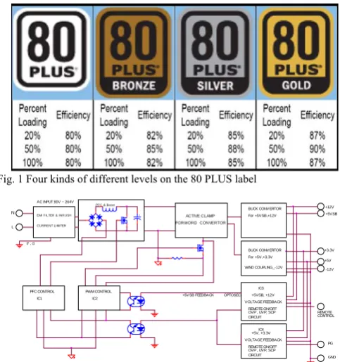
The EPA (Environmental Protection Agency) regulation was implemented in California of U.S.A. since 2003. It specifically indicated that the multiple output power supply in 20%, 50% and 100% specified load used by work stations, PC’s, and servers need to be 80% or higher energy efficiency, besides, the power factor must be greater than 0.9. In addition, to distinguish the efficiency, there were four kinds of different levels on the 80 PLUS label from 2008, as Fig. 1. Therefore, low price with high efficiency becomes the goal of every power supply manufacturer at present.
In various voltage converters, only the circuit scheme that has soft switching technology could meet the demands. As for medium-high exportation output power, the Active Clamp Forward Converter needs only two switch components to meet the economic benefits relatively. Therefore, according to this special circuit scheme, I make one direct-current power supply with characteristic of zero voltage switching that performs high efficiency and high power density.
The circuit block diagram of the power module discussed in this paper is as following Fig. 2. The output voltages are regulated via two secondary control IC’s, the IC3 and the IC4.
Chia-Sheng Tsai is with Dept. of CSE, Tatung University, Taipei, Taiwan (R.O.C.) (corresponding author, phone: +886-2-2182-2928 ext. 6552; e-mail: [email protected]).
Ming-Yang Tsai, was graduated from Tatung University. He is now with LITE-ON Technology Corp. and going to study in Virginia Polytechnic Institute and State University, USA.
Ming-Chieh Tsai is with the Electrical Engineering Department, Tatung University, Taipei, Taiwan (R.O.C.).
The ideal secondary bi-directional switches are realized by two external MOSFETs in anti-series. The bi-directional switches of 3V3 and 5V outputs are partly shared.
The bi-directional switch of the standby output consists of a diode in series with a FET instead of two MOSFETS in anti-series. All control IC’s have integrated drivers, therefore the external MOSFETS can directly be connected to the control IC’s.
[image:1.595.307.549.506.764.2]The IC3 is the master of the system and defines the mode of operation. Depending on the PS_ON# signal and input voltage (via the EN_NM pin) the system is either in standby or normal operation. In case of a fault condition, OCP, OVP or OTP, the system will switch to standby mode independently of the PS_ON# signal. By toggling the PS_ON# signal the system will switch to normal mode again, of course under the requirement of a minimum input voltage. Via the enable signal the mode of operation is communicated from the IC3 to the IC4. A possible fault on the 3V3 or 5V output is communicated from the IC4 to the IC3 via the same wire. Via a photo-coupler mode of operation is communicated to the primary side. Each output has OCP and OVP protection [1]. And also using Power Factor Correct (PFC) circuit reduces Total Harmonic Distortion (THD) of the power module and improves the Power Factor (PF) value. Certainly, in respect of energy efficiency, it must meet the demand of 90%.
Fig. 1 Four kinds of different levels on the 80 PLUS label
. . . IC3 +5VSB, +12V +5VSB
EMI FILTER & INRUSH PFC & Boost
BUCK CONVERTOR AC INPUT 90V ~ 264V
+3.3V PWM CONTROL FORWORD CONVERTOR N +5V, +3.3V L IC4 IC2 GND CURRENT LIMITER IC1 . . . VOLTAGE FEEDBACK ACTIVE CLAMP +12V PG CONTROL REMOTE -12V
+5VSB FEEDBACK OPTOSEC For +5VSB,+12V WIND COUPLING_-12V For +5V,+3.3V BUCK CONVERTOR + REMOTE ON/OFF OVP , UVP, SCP CIRCUIT PFC CONTROL
+5V
OVP , UVP, SCP CIRCUIT REMOTE ON/OFF VOLTAGE FEEDBACK
F.G
Fig. 2 Circuit configuration of active-clamping ZVS forward converter for the standard ATX80+
Design of Clamp Forward Converter Used in
Computing Devices
II. PRINCIPLE OF OPERATION
A. TWO-STEP FOLLOWER PFC
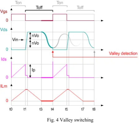
The PFC operates in Quasi Resonant (QR) or Discontinuous Conduction Mode (DCM) with valley detection to minimize switch-on losses. The maximum switching frequency of the PFC is limited to 125 kHz to reduce switching losses. One or more valleys are skipped, when necessary, to keep the frequency below 125 kHz [2].
The PFC is designed as a dual boost converter with two output voltage levels that are dependent on the mains input voltage range. The advantage of such a dual boost is that overall system efficiency at low mains can be improved due to reduced PFC switching losses.
The special built-in green functions provide high efficiency at all power levels. This applies to quasi-resonant operation at high power levels and quasi-resonant operation with valley skipping, model is shown as Fig. 3.
Voutsense
R115 AC INLET
L FG N
PFCsense
GND 1
Vinsense 2
PFCCOMP 3
PFCAUX 4
Vcc 8 PFCDRV 7 PFCSENSE 6 VOsense 5
R2 68K
P
R1
@ 9.9M
- +
2
1
3
[image:2.595.51.286.310.460.2]4 . .
Fig. 3 PFC circuit model
The PFC MOSFET is switched on after the transformer is demagnetized in Fig. 4. Internal circuitry connected to the PFCAUX pin detects- -the end of the secondary stroke. It also detects the voltage across the PFC MOSFET. The next stroke is started if the voltage across the PFC MOSFET is at its minimum in order to reduce switching losses.
voltage. The mains input voltage is measured via the VINSENSE pin. The current is sourced from the VOSENSE pin if the voltage on the VINSENSE pin drops below 2.5V. For low VINSENSE input voltages, the output current is 8μA. This output current, in combination with the resistors on the VOSENSE pin, sets the lower PFC output voltage level at low mains voltages, as in (1). At high mains input voltages the current is switched to zero. The PFC output voltage will than be at its maximum. As this current is zero in this situation, it does not affect the accuracy of the PFC output voltage and show in table 1.
) 8 ( 2
2
1 uA
ref ref
boost I
R V R V
V ⎟⎟ −
⎠ ⎞ ⎜⎜
⎝ ⎛ +
= (1)
Table 1 Dual boost voltage PFC Boost Voltage Input VAC 230 VAC 115 VAC
Vosense-R1 10000K 10000K OHM
Vosense-R2 67K 67K OHM
I 0 8 u A
Vref 2.5 2.5 V
Boost Voltage 380 296 V
The PFC efficiency is better than 95% and the power factor also can higher than 0.9, show in table 2.
Table 2 PFC efficiency PFC Efficiency @ output load 255w
Input Voltage 20% 50% 100%
100 95.60% 95.60% 94.50%
115 95.90% 96.10% 95.40%
230 95.90% 97.00% 97.30%
B. ACTIVE-CLAMPING ZVS FORWARD CONVERTER
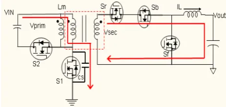
Fig. 2 shows the circuit configuration of the adopted active-clamping ZVS forward converter. The Green Chip PC controlled switch concept integrates the standby supply into the main converter, reducing the overall costs. By replacing the secondary rectifying diodes (DR) with (bi-directional) switches the standby voltage can be realized by adding an extra winding on the main transformer, show as Fig. 5. As these switches have to withstand and be able to block positive and negative voltages, these are called bi-directional switches. In standby mode the main output (3V3, 5V and 12V) are disabled by these bi-directional switches. To increase overall efficiency, the diodes (DF) are replaced by rectifying MOSFETS [3]-[6].
[image:2.595.60.285.569.767.2]Fig. 5 Schematic of the green chip PC concept
Shown in the Figure of Fig. 5 to Fig. 13, the “ideal” bi-directional switch described in the “Theory of Operation” is in practice build up by two standard FETs in anti-series. Two FETs are required because of their back-gate diode. As the output current of a PC power supply is of such a high value that switching off switch SB, while it is conducting this high current, causes enormous voltage spikes. These spikes, mainly caused by the leakage inductance of the transformer, can be hundreds of voltage and will therefore harm the application. The paragraph describes a procedure of switching the secondary switches in such a way that voltage spikes are prevented under all circumstances. And therefore the breakdown voltage of the applied switches can be minimized [8]-[12].
The primary switch S1, SR and SB are closed. Switches SF and S2 are open. As switch S1 is closed, the secondary voltage equals Vin/N whereas N is np/ns (number of primary win- dings / number of secondary windings). Cause of the positive voltage across the output inductor, its current is increasing at a rate equal to (Vin/N – Vout).
Fig. 6 The ideal bi-directional switch control
[image:3.595.312.548.162.268.2]The primary switch S1 is turned off. The parasitic capacitance of S1, Cs, will be charged by the reflected output current (Iout / N) and the magnetizing inductance current ILM. The secondary switches stay unchanged.
Fig. 7 The ideal bi-directional switch control
[image:3.595.313.547.384.490.2]Once the voltage across S1 reaches the input voltage, the voltage at the transformer (Vprim and Vsec) is zero. At this time SR is turned off and the output current commutates from SR / SB to SF. Because of parasitic inductances, the output current flows for a certain time through both output switches. During this time the voltage at the secondary side of the transformer stays zero. The primary side magnetizing current will start to charge the reset capacitor.
Fig. 8 The ideal bi-directional switch control
The output current entirely flows through SF and the secondary transformer voltage will be negative. At this time SF is turned on and SB is turned off. Switch SR was already turned off. Cause of the negative voltage across the output inductor, its current will decrease at a rate equal to –Vout / L. A certain time after the current starts to flow through the parallel diode of S2, this switch is turned on.
Fig. 9 The ideal bi-directional switch control
At a certain time, the charge current to the reset capacitor reaches zero. Because the reset capacitor is charge to a VRESET voltage and S2 is on, the current will change polarity.
Fig. 10 The ideal bi-directional switch control
[image:3.595.55.288.495.599.2] [image:3.595.313.548.569.676.2] [image:3.595.56.288.679.789.2]Fig. 11 The ideal bi-directional switch control
When the voltage across S1 becomes zero, the primary switch is turned on again.
Fig. 12 The ideal bi-directional switch control
[image:4.595.309.549.55.362.2]When the bidirectional switch SB is switched on (and SF is switched off (switching of SF is the inverse of SB)), the transformer is short circuited and the output current commutates from the freewheel switch SF to the bidirectional switches (SR and SB). As the switches SR and SF are off, the current will flow via its back gate diode. The commutation time depends on the leakage inductance and the value of the output current. Remark: After commutation the leakage inductance resonates with the parasitic capacitances (of SF and of the transformer). Because of the limited breakdown voltage of the secondary switches, this resonance needs to be clamped.
Fig. 13 The ideal bi-directional switch control
After the commutation period the secondary side transformer voltage will equal Vin/N again. SR is turned on after this commutation period, detected by a positive VHB voltage (half bridge voltage is the voltage at the drain of Sf).In this way the output voltage depends on the duty cycle of secondary switch SB and not on the duty cycle of the primary main switch S1. Switches SR and SF actually act like a diode, but are switches to reduce the conduction losses.
[image:4.595.55.289.214.320.2]III. THE MEASUREMENT RESULTSUS
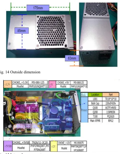
Fig. 14 Outside dimension
Fig. 15 Internal components
To verify the feasibility of the proposed energy-saving, active-clamping ZVS forward converter with two-step follower boost MOSFETS, following specifications are implemented and tested. The testing results are shown in Table 3 and Table 4. The finally modified board was implemented, as Fig. 15.
z Universal input voltage range: 90VAC ~ 264 VAC z Input Frequency range: 47 Hz ~ 63 Hz
z Output voltages: 12VO/18A, 5VO/15a,
3.3VO/10A, -12VO/0.5A, 5VSB/4A z Mains Harmonics: ACC. To EN61000-3-2
[image:4.595.303.533.458.778.2]z Overall Efficiency: Better than 87% TABLE 3 Part count
Converter Part Count
Active Clamp Forward Converter 277 Pcs
LLC Converter 422 Pcs
TABLE 4 Efficiency performance
Load (%) VAC PF Efficiency (%) SPEC
(%)
115 0.95 88.48 87
20
230 0.875 87.79 87
115 0.98 90.83 90
50
230 0.915 91.76 90
115 0.99 88.14 87
[image:4.595.56.287.494.599.2]IV. CONCLUSION
This paper has proposed several circuits for converters to achieve the gold standard ATX80+. A two-step follower boost MOSFETS performs higher power factor and, higher efficiency during input VAC of low and high line. The design procedures are also formulated and justified. The experimental results of a 255 watts power supply are implemented. The average efficiency is 89.6%, and the maximum efficiency is 91.76%. For universal AC input, active-clamping ZVS forward converter perform the maximum duty is over 50%, and limit the voltage stress of the switches. For designer engineers, the proposed new technologies might be adopted to original power module, in which to be easier to meet the EPA regulation.
REFERENCES
[1] P. LARO, Green chip PC introduction NXP Semiconductors. http://www.nxp.com/#/homepage/cb
[2] NXP semiconductors, TEA1742 PFC controller, Data sheet. http://www.nxp.com/search/?query=tea1742
[3] NXP semiconductors, TEA1771 PFC controller, Data sheet. http://www.nxp.com/search/?query=tea1771B
[4] H. K. Ji and H. J. Kim, “Active clamp forward converter MOSFET synchronous rectification”in Proc. IEEE Int. Conf. Power Electronics Specialists, vo1. 2, pp. 895 – 901, June 1994
[5] J. A. Cobos, O. Garcia,J. Sebastian, J. Uceda, “Active clamp PWM orward converter with self driven synchronous rectification” in Proc. IEEE Int. Conf. Telecommunications Energy, vol. 2, pp. 200-206 , Sept. 1993.
[6] Q. M. Li, F. C. Lee, M. M. Jovanovic, “Large-signal transient analysis of forward converter with active-clamp reset”, in Proc. IEEE Int. Conf. Power Electronics, Vol.17,1993, pp.15-24.
[7] A. Acik and I. Cadirci, “Active clamped ZVS forward converter with soft-switched synchronous rectifier for maximum efficiency operation”, in Proc. IEEE Int. Conf. Power Electronics, Vol. 2,pp. 1237 – 1242, May 1998.
[8] C. H. Wu, Stability Study of Active-Clamp Forward Converters, Master Thesis, Department of Electrical Engineering, I-Shou University, Taiwan, 2003.
[9] K. Y. Liu, Utilization of an active-clamp circuit to achieve soft switching in back converters, Master Thesis, Department of Electrical Engineering, Tatung University, Taiwan, 2000.
[10] H. C. Chang, Analysis and Implementation of Active- Clamp Forward Converters with Synchronous Rectification, Master Thesis, Department of Electrical Engineering, Kun Shan University, Taiwan, 2007.
[11] NXP semiconductors, TEA1781/82 PFC controller, Data sheet. http://www.nxp.com/search/?query=tea1781