c
A HIERARCHICAL ADAPTIVELY BOOSTED IN-MEMORY CLASSIFIER IN 6T SRAM
BY SUNGMIN LIM
THESIS
Submitted in partial fulfillment of the requirements
for the degree of Master of Science in Electrical and Computer Engineering in the Graduate College of the
University of Illinois at Urbana-Champaign, 2019
Urbana, Illinois Adviser:
ABSTRACT
Recent emerging machine learning applications such as Internet-of-Things and medical devices require to be operated in a battery-powered platform. As the machine learning algorithms involve heavy data-intensive computa-tions, interest in energy-efficient and low-delay machine learning accelerators is growing. Because there is a trade-off between energy and accuracy in ma-chine learning applications, it is a reasonable direction to provide scalable architecture which has diverse operating points.
This thesis presents a high-accuracy in-memory realization of the Ad-aBoost machine learning classifier. The proposed classifier employs a deep in-memory architecture (DIMA), and employs foreground calibration to com-pensate for PVT variations and improve task-level accuracy. The proposed architecture switches between a high accuracy/high power (HA) mode and a low power/low accuracy (LP) mode via soft decision thresholding to pro-vide an elegant energy-accuracy trade-off. The proposed realization achieves an EDP reduction of 43X over a digital architecture at an iso-accuracy of 95% for the MNIST dataset, which is an improvement of 5% over a previous in-memory implementation of AdaBoost.
ACKNOWLEDGMENTS
I sincerely feel gratitude toward my adviser, Prof. Naresh R. Shanbhag, for his support and guidance. I would also like to extend my gratitude to Sujan Gonugondla, Ameya Patil, and Charbel Sakr for helpful discussions. I would like to give special thanks to Mingu Kang and Yongjune Kim for strong support in various aspects. I was lucky to join a research group in which I could experience active discussions in group meetings and have healthy interactions with group members for my individual growth. This work was supported by Systems On Nanoscale Information Fabrics (SONIC), one of the six SRC STARnet Centers, sponsored by SRC and DARPA.
TABLE OF CONTENTS
LIST OF FIGURES . . . vi
LIST OF ABBREVIATIONS . . . viii
CHAPTER 1 INTRODUCTION . . . 1
1.1 Motivation . . . 1
1.2 Related Work . . . 2
1.3 Thesis Contributions and Organization . . . 3
CHAPTER 2 BACKGROUND . . . 5
2.1 Deep In-memory Architecture (DIMA) . . . 5
2.2 Adaptive Boosting (AdaBoost) . . . 8
CHAPTER 3 DIMA-BASED ADABOOST ARCHITECTURE . . . . 10
3.1 Implementation Challenges . . . 10
3.2 Proposed In-memory Architecture . . . 10
3.3 Circuit Design . . . 13
3.4 Retraining with Foreground Calibration . . . 17
CHAPTER 4 MEASUREMENT RESULTS . . . 18
4.1 Component-level Accuracy . . . 18
4.2 Task-level Accuracy and Energy . . . 21
CHAPTER 5 CONCLUSION AND FUTURE WORK . . . 25
5.1 Conclusion . . . 25
5.2 Future Work . . . 25
LIST OF FIGURES
1.1 Simplified von Neumann machine-based inference. . . 2 2.1 DIMA and data-flow. . . 6 2.2 Conventional digital hardware: (a) Conventional digital
ar-chitecture, and (b) data-flow. . . 6 2.3 DIMA multi-row functional read (B = 4). . . 7 2.4 10-class classifier with 45 strong classifiers. . . 9 3.1 Multi-class AdaBoost classifier: top-level architecture with
M = 256 weak classifiers per strong classifier and N = 45
strong classifiers. . . 11 3.2 Proposed AdaBoost modes: the low-power (LP), high
ac-curacy (HA), and hybrid modes in a strong classifier. . . 11 3.3 Proposed in-memory AdaBoost hardware architecture with
HA and LP modes. . . 14 3.4 In-memory comparison with analog comparator and timing
diagram. . . 15 3.5 Replica bit-cell circuit configuration. . . 16 3.6 The foreground calibration process to compensate for
bit-cell variations. . . 17 4.1 Chip micrograph and measurement setup. . . 19 4.2 Measured results (◦: q = 0, •: q = 1) of the first and
second weak classifiers at: (a) ∆Vlsb = 25 mV, and (b)
∆Vlsb = 15 mV, where each dot corresponds to one of the
MNIST test images for the number 3 and 5. . . 20 4.3 Measured results with (without) foreground calibration:
comparator error rate vs. misclassification rate w.r.t. ∆Vlsb
for MNIST dataset. . . 21 4.4 Measurement results: error rate vs. ∆Vlsb for HA mode
and LP mode. . . 22 4.5 Misclassification rate vs. energy in HA mode and LP mode. . 23 4.6 Error rate vs. average energy in hybrid mode in two
config-urations: C1=[∆Vlsb(LP) = 15 mV; ∆Vlsb(HP) = 30 mV]
4.7 Accuracy vs. EDP for 10-class MNIST dataset.
LIST OF ABBREVIATIONS
AdaBoost Adaptive Boosting BCA Bit-cell array
BL Bit-line
BLB Bit-line bar
BLP Bit-line processing CBLP Cross bit-line processing DIMA Deep in-memory architecture
ML Machine learning
SNR Signal-to-noise ratio
SRAM Static random-access memory
CHAPTER 1
INTRODUCTION
1.1
Motivation
The high energy and delay costs of current day machine learning (ML) algo-rithms inhibit their deployment for real-time always-on inference on sensor-rich platforms such as wearables, UAVs, personal biomedical devices, Internet of Things (IoT), and many others. In such systems, the data movement dom-inates the high energy and latency cost [1]. As a result, energy-efficient and low-latency machine-learning hardware is required to sustain the always-on functionality (e.g. face detection) amid resource constraints such as limited form factor for mobility, processing time for real-time streamed-in input data, and energy for battery-powered platform (Fig. 1.1). However, the current ML platforms (e.g. CPU, GPU, and FPGA) based on von Neumann architec-ture [2] are not suitable in the battery-powered hardware due to their high data movement cost [3].
A number of machine learning accelerators [4–10] to reduce the data move-ment cost using data reuse methods have been proposed, but these target the server platform and are limited by the memory-processor interface. There-fore, overcoming von Neumann structure should be the first step to build a data-intensive computing architecture for the emerging applications. Ad-ditionally, there is a fundamental trade-off between energy and accuracy in most ML applications. Therefore, it is a reasonable direction to implement scalable architecture with a wide spectrum of operating points because all the applications do not necessarily require highly accurate networks with large energy consumption.
Inference
Engine
Memory
WeightsDog, Cat
Input stream
Output streamFigure 1.1: Simplified von Neumann machine-based inference.
1.2
Related Work
Recently, in-memory architectures [1, 11–14] were proposed to address the data movement cost. Such architectures embed low-swing analog computa-tions in the periphery of the SRAM bit-cell array (BCA) to minimize memory access rates, substantially reducing the energy-delay product (EDP) of in-ference, but can lead to degradation in task-level accuracy due to circuit non-idealities such as Vt variations in the bitcell array (BCA). Nevertheless,
IC prototypes have realized up to 100×reduction in the energy-delay product (EDP) [12] at iso-accuracy with digital architectures.
The multi-functional in-memory inference processor [1] and the random forest accelerator [11] achieve significant gains in the energy efficiency (10×) and throughput (5.3×) over a conventional digital architecture by exploiting the inherent error tolerance of machine learning algorithms. In contrast, [12] shows that training with chip-in-the-loop can improve DIMA’s accuracy but at the expense of a large retraining overhead, e.g., requiring 6400 images for binary classification. On the other hand, [11] implemented the random forest algorithm on DIMA using an embedded crossbar for feature extraction to achieve high accuracy in an 8-class traffic sign recognition task. However, the crossbar can be too complex to be employed in always-on applications.
For the always-on IoT applications, the AdaBoost [15] algorithm is attrac-tive due to its low computational complexity and good accuracy. In spite of its simplicity, not much work has been done on realizing the AdaBoost algorithm using in-memory architectures except for [13]. In [13], a 10-class in-memory AdaBoost classifier [13] achieved an energy efficiency of 630 pJ per decision. However, the achievable accuracy was limited to 90% for the MNIST dataset, which was improved to 91% via the use of four in-memory ICs [16] indicating the challenge of improving the task-level accuracy of Ad-aBoost using in-memory architectures. Also, 25% of SRAM bit-cells had to be allocated to compensate for comparator offsets, compromising the memory density [13, 16].
As another approach for an efficient architecture, there are a number of at-tempts to build the scalable hardware which have a trade-off between energy, delay and accuracy. Dynamic Voltage-Accuracy Scaling (DVAS) [17] exploits shorter critical paths combined with lower precision for scaled voltage. As a next version, Dynamic Voltage-Accuracy-Frequency Scaling (DVAFS) [7] made additional frequency scaling possible. Precision scaling [6, 7, 17] is widely used with masking input or weight bits. Lastly, hierarchical recogni-tion by [7] provides increasing numbers of classes as it goes to last recognirecogni-tion stage with growing complexity. As an orthogonal way of scaling, this thesis proposes hybrid mode using soft decision value to determine an operating point.
1.3
Thesis Contributions and Organization
This thesis proposes a hierarchical architecture to realize in-memory Ad-aBoost with improved accuracy for always-on applications using decision tree-based weak classifiers. The proposed architecture computes a soft deci-sion margin in its low-power/low-accuracy model (LP mode), and switches to a high-accuracy/high-power mode (HA mode) only when the confidence level indicated by the soft decision margin in the LP mode is low. The pro-posed architecture is experimentally validated via test configurations of a previously reported IC [11] using 8-b precision for both weights and input pixels. The proposed in-memory AdaBoost realization achieves a 43× re-duction in EDP at an iso-accuracy of 95% over a digital neural network [18].
This is a 5% improvement in accuracy over the previous in-memory AdaBoost implementation [13] though at a higher EDP.
This remainder of thesis is organized as follows. Chapter 2 explains back-ground for DIMA and AdaBoost. Implementing the AdaBoost algorithm on DIMA, the proposed architecture, and foreground calibration techniques are described in Chapter 3. The measurement results including energy, through-put, and accuracy from both component-level and task-level are described in Chapter 4. Finally, Chapter 5 concludes the thesis.
CHAPTER 2
BACKGROUND
2.1
Deep In-memory Architecture (DIMA)
2.1.1
DIMA Overview
This thesis employs the DIMA platform to implement an energy-efficient and low-latency AdaBoost algorithm accelerator. DIMA reads multiple rows of a standard 6T SRAM bitcell array (BCA) per precharge via pulse width modulated (PWM) wordline (WL) pulses to read word-level information. This stage is called multi-row functional read [1]. It processes the consequent bitline (BL) voltage drops ∆VBL via column pith-matched bitline processor
(BLP) in the periphery of the BCA (Fig. 2.1).
The BLP computes scalar distances such as multiplication and scalar com-parison. Following BLP output is aggregated in the cross bitline processing stage for dimension reduction operation (e.g. sum). This work uses BLP as scalar comparison for thresholding.
While the conventional SRAM architecture requires a L : 1 column mux ratio (typically L = 4 to 32) due to large area of sense amplifiers (SA) as shown in Fig. 2.2, DIMA does not require SAs to read memory because it directly uses ∆VBLwithout massive data transfer [1, 11]. Column mux limits
the number of bits per access to NCOL/L in standard SRAM compared to NCOL×4 in DIMA with multi-row read as shown in Fig. 2.1. As a result,
DIMA reduces dominant memory access cost in computations [3] compared to the conventional digital architecture. Comparing data-flow conventional digital architecture (Fig. 2.2) and DIMA (Fig. 2.1), it is clear that DIMA has fewer intermediate steps than the digital architecture. This implies that DIMA has strong benefits in terms of energy and delay.
word row (4 rows) word MSB T LSB
SRAM array (NROW x NCOL)
Input BLP output Analog Computation B LP BLP BLP BLP BLP LPB BLP BLP BLP BLP BLP
Bit-cell Array
(BCA)
Analog
Processor
Analog
(a)
(b)
Figure 2.1: Proposed in-memory computing hardware: (a) DIMA [1, 11], and (b) data-flow.
On-chip
SRAM array (NROW x NCOL)
L:1 L:1 L:1 SA SA SA 1 0 1 e.g. 1-bit digital
(NCOL / L) bits fetched per access T VBL: 1-bit analog Word 1 Word 2 Word 3 Word 4 Word 5 Word 6 Word 7 Word 8 data bus P ro c e s s in g e le m e n t Digital Computation Buffer
Bit-cell array (BCA)
Data BUS Processor buffer Processing element Digital L:1 MUX
Sense amplifier (A2D)
Analog
(a)
(b)
Figure 2.2: Conventional digital hardware: (a) Conventional digital architecture, and (b) data-flow.
BLB
BL
...
...
d
0d
1d
2d
3 P u ls e-W id th M o d u la ti o n ΔVBLBWL
0WL
1WL
2WL
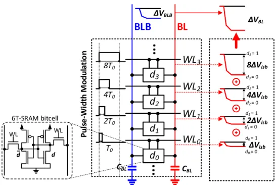
3 T0 2T0 4T0 8T0 6T-SRAM bitcell WL WL d d 8ΔVlsb 4ΔVlsb 2ΔVlsb ΔVlsb ΔVBL d3 = 0 d3 = 1 d2 = 0 d2 = 1 d1 = 0 d1 = 1 d0 = 0 d0 = 1 CBL CBLFigure 2.3: DIMA multi-row functional read (B = 4).
2.1.2
Multi-row Functional Read
The multi-row functional read (Fig. 2.3) creates voltage drop ∆VBL which is
proportional to B-bit word data D(= PB−1
i=0 2
id
i) stored in column-major.
The ∆VBL(D) can be fomulated as:
∆VBL(D) = VP RE RBLCBL T0 B−1 X i=0 2i−1di = ∆VlsbD,
where VP RE is BL precharge voltage, RBL is resistance of the BL discharge
path via the access and pull-down NMOS transistors, CBL is BL parasitic
capacitance, and T0 is minimum pulse width enabled on WL. Here, Dis the
integer number of one’s complement ofD. The unit BL voltage drop ∆Vlsb = VP RE
RBLCBL is a function of WL voltage VW L asRBL depends on VW L. As ∆VBL
is closely related to energy consumption, VW L can be used to implement
2.2
Adaptive Boosting (AdaBoost)
The ensemble classifier is one of the machine learning classification algo-rithms. The ensemble methods create a strong classifier by combining weak classifiers which are inaccurate with around 50% detection failure rate. An analog circuit can exploit this property because the analog computations are usually faster and lower energy, but less accurate, than digital implemen-tations. Therefore, designing a weak classifier in analog domain can take advantage of ensemble classification.
AdaBoost, as an ensemble method, adds the weak learners iteratively to build a highly accurate network by training the weak learners on differ-ent distributions over the example dataset. Let us say training examples h(I1, y1), (I2, y2), ..., (Im, ym)i are given, where Ii ∈I is an image sample in
the training setIandyi ∈ {−1,+1}is a label. In the first step, a distribution D1 on the training set is initialized as:
D1(i) = 1/m, ∀i= 1, ..., m.
The distribution Dis used to give different weighting distributions on exam-ples at each training sequence. In the t-th iteration, a current weak learner focuses on misclassified input images in the previous iteration in order to re-duce the same errors at a subsequent learner by weighting the failed images, namely adaptively boosting. Given an input set, the t-th weak classifier qt
is trained to minimize the weighted error t, which is a sum of the product
of the i-th weak hypothesisqt(Ii)∈ {−1, +1} error and thei-th distribution Dt(i) in thet-th iteration: t = m X i=1 Dt(i)·1[qt(Ii)6=yi].
Once the t is determined, AdaBoost chooses a parameter αt as follows: αt= 1 2ln( 1−t t ).
The higher value of αt means that the t-th weak classifier is more reliable,
having high impact on a final (strong) classification. In the next iteration, AdaBoost updates the distribution Dt toDt+1 for i= 1, ..., m as follows:
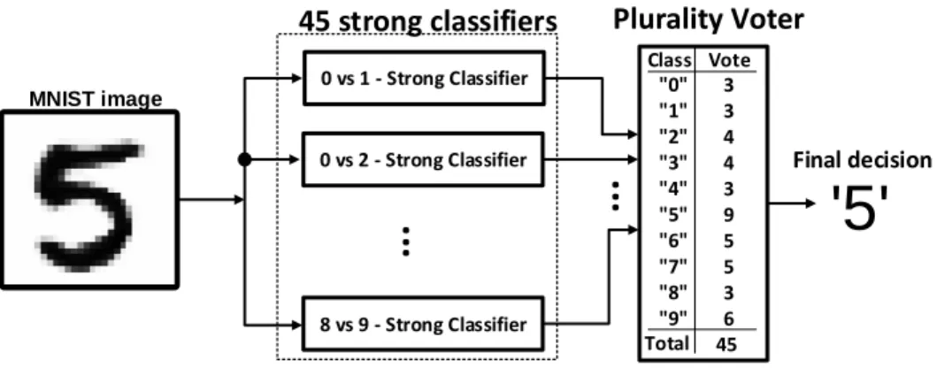
0 vs 2 - Strong Classifier 8 vs 9 - Strong Classifier
...
Plurality Voter...
MNIST image'5'
Final decision 0 vs 1 - Strong Classifier 45 strong classifiers Class "0" "1" "2" "3" "4" "5" "6" "7" "8" "9" Vote 3 3 4 4 3 9 5 5 3 6 Total 45Figure 2.4: 10-class classifier with 45 strong classifiers.
Dt+1(i) =
Dt(i)exp(−αtyiqt(Ii))
Zt
,
where Zt is a normalization factor: Zt =
m
X
i
Dt(i)exp(−αtyiqt(Ii)).
Finally, during inference, a test image Ij is classified as:
ˆ y(Ij) = sign( M X t=1 αtqt(Ij)),
where M is a total number of weak classifiers.
This thesis employs a simple comparison between a pixel value and a trained threshold as a single weak classifier in AdaBoost inference, result-ing in binary output qt. In order to build a 10-class classifier, the C210 = 45
strong binary classification results are computed using the one-vs.-one strat-egy. Note that the one-vs.-one strategy only distinguishes two classes (binary decision). As shown in Fig. 2.4, the strong binary decisions from the 45 one-vs.-one classifiers are fed into a plurality voter and the final decision (e.g., 5) is made.
CHAPTER 3
DIMA-BASED ADABOOST
ARCHITECTURE
3.1
Implementation Challenges
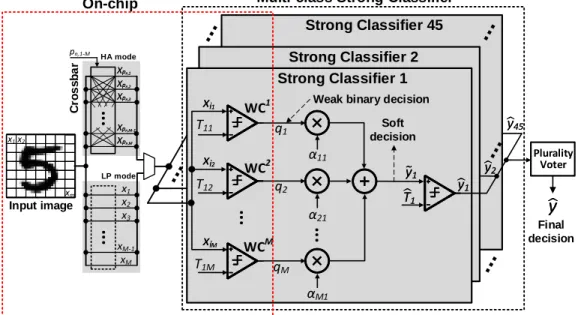
Implementing a multi-class inference system in-memory using AdaBoost with decision trees presents the following challenges: (1) Crossbar cost: Each strong classifier (Fig. 3.1) needs to use a different subset of features necessitat-ing a crossbar whose complexity increases with feature dimension. (2)Circuit non-idealities: DIMA is vulnerable to various circuit non-idealities such as PVT variations and non-linearity due to low-voltage analog operations. (3) Retraining complexity: Retraining to overcome circuit non-idealities incurs significant complexity overhead, e.g., 25% of memory capacity [13] devoted to offset calibration, and massive retraining dataset [12]. By implementing Ad-aBoost on the in-memory architecture IC [11], this work demonstrates the benefits of exploiting the intrinsic error-tolerance of an ensemble classifier and the energy-efficiency of a mixed-signal implementation.
3.2
Proposed In-memory Architecture
The proposed architecture in Fig. 3.1 realizes a 10-class classifier output ˆy by plurality voting the outputs ˆyn(n = 1, . . . , N = 45) ofN =C210 = 45 boosted
(strong) binary classifiers. The n-th strong classifier’s output obtained is ˆ
Strong Classifier 45 T11 T12 T1M α11 α21 αM1
..
.
WC1 WC2 WCM..
.
Input image Final decision Weak binary decisionStrong Classifier 1 x1x2 xm xi1 xi1 xi2 xi2 xiM xiM C ro s s b a r pn,1-M
..
.
pn,1 Xpn,1 X pn,2 Xpn,2 X pn,3 Xpn,3 X pn,M-1 Xpn,M-1 X pn,M Xpn,M X..
.
x2 x3 xM-1 xM x1 HA mode LP mode Soft decision q1 q2 qM T1 T1 y45 y45 y1 y1 Strong Classifier 2 Plurality Voter y2 y2 y1 y1y
y
Multi-class Strong Classifier On-chip
Figure 3.1: Multi-class AdaBoost classifier: top-level architecture with
M = 256 weak classifiers per strong classifier and N = 45 strong classifiers.
LP mode
Crossbar Input XHA mode
hybrid mode
y n yn yn yn 1 0 SDM > Th SDM = |yn – Tn| 1 0
margin
thresholding
Strong ClassifierFigure 3.2: Proposed AdaBoost modes: the low-power (LP), high accuracy (HA), and hybrid modes in a strong classifier.
where Tbn is the strong classifier threshold, and the soft decision y˜n is com-puted as ˜ yn = 256 X m=1 αnmqnm. (3.2)
Here, αnm’s are the trained strong classifier parameters, and qnm (n =
1, . . . ,45;m= 1, ...,256) are the weak classifier decisions obtained as:
qnm = 1 if Tnm > Xi 0 otherwise, (3.3)
where Tnm is the trained pixel threshold of the m-th weak-classifier within
the n-th strong classifier, and Xi is a pixel with index i ∈[1,256]. Though
each weak classifier has low accuracy, e.g., slightly greater than 50%, each strong classifier generates a > 90% accuracy. Plurality voting of 45 such strong binary classifiers generates the final 10-class prediction. Each weak classifier is a scalar comparator that compares pixelXiwith a pixel threshold Tnm via in-memory computations in [11], thereby addressing challenges (2)
and (3) in section 3.1. Using scalar comparators as weak classifiers enables simple foreground calibration, where the threshold and all possible pixel val-ues are compared in-memory to retrain the thresholds. In this manner, the comparator offset and bit-cell variation are compensated for without requir-ing complex gradient descent based approaches [12,13] with massive trainrequir-ing datasets.
Challenge (1) is addressed by introducing three strong classifier modes (Fig. 3.2): (a) a high-accuracy (HA) mode by realizing a many-to-one map-ping of pixels to a threshold via a crossbar, (b) a low-power (LP) mode by realizing a one-to-one mapping of pixels to a threshold bypassing the cross-bar to achieve energy and delay efficiency at the cost of accuracy, and (c) a hybrid mode to obtain the energy-efficiency of the LP mode and accuracy of the HA mode by selectively enabling crossbar using soft decision margin (SDM =|y˜n−Tbn|) of the LP mode (Fig. 3.2). Here, the LP mode works as analways-on early detector to filter binary decisions of the strong classifiers which have SDM < Th (low-confidence decisions), where Th is the margin
soft decision margin in the LP mode is low. Challenge (1) in the HA mode is further addressed by deterministic sub-sampling (DSS) [11], where four groups of weak classifiers are constrained to use a dedicated one-of-four 4:1 sub-sampled input images. Therefore, a single 256:1 crossbar can be re-placed by four 64:1 crossbars achieving significant complexity reduction with less than 0.2% accuracy degradation.
3.3
Circuit Design
The proposed 10-class classifier (Fig. 3.3) includes a SRAM BCA to store pretrained 8-b thresholds THA
nm, TnmLP and 6-b pixel index pn,m, multi-row
wordline (WL) drivers, 64-b I/O with a 4:1 column mux, DSS input buffer to store streamed-in 256 8-b pixels Xi, four 64:1 crossbars, and peripherals
for standard read/write operations. The LP and HA modes use TnmHA and
TnmLP, respectively, to classify an image. The crossbar is enabled only in the HA mode and routes pixels to replica bit-cell array via the pixel index pn,m
which is stored in the BCA at the start of in-memory comparison [11]. In-memory comparison (Fig. 3.4) [11] begins by storing the 128 pixels ofX
into the replica BCA, which is designed to write the 8-b pixels Xi efficiently
by having additional write BL with access transistors. Storing the X in the replica BCA (Fig. 3.5) allows fast writing through a separate write BL (WBL) and wordline (WWL) by eliminating the overheads of slow write operation into normal BCA. The multi-row WL driver applies binary pulse-width mod-ulated pulses simultaneously toW L3−0 andRW L3−0 to discharge BL (BLB)
creating voltage swing ∆VBL(∆VBLB) proportional to X−T(T −X). Here,
linearity of the multi-row read is improved by reading 4-b MSBs and LSBs separately from adjacent columns followed by a capacitively weighted charge sharing that assigns 16× greater weight to the MSBs. The WL voltage is reduced (e.g. 0.65 V) to prevent destructive read and further improve the linearity.
Finally, in-memory comparison phase generates 128 binary weak decisions
qn1∼128, requiring two such cycles to compute one strong classifier decision ˆyn.
After 90 such in-memory cycles, the final multi-class decision ˆy is generated via plurality voting the 45 binary strong decisions ˆyn. The computation of
˜
Mu lt i-ro w W L dr iv e r w / ro w d ec . Mu lt i-ro w W L dr iv e r w / ro w d ec . Plurality Voter αmn q[1:128] D O ff -c hi p po st p ro ce ss in g
4×256 SRAM Replica bit-cell array 4×256 SRAM Replica bit-cell array
Normal read/write circuitry Normal read/write circuitry 6-T SRAM bit-cell array
"0" vs "1" Input buffer (X) X1,5,…,253 BLs BLs BLs BLs "0" vs "2" "8" vs "9" CB 64x 32 64x 32CB 64x 32CB 64x 32CB C ro ss b ar s w it ch x(pn,m) 128 Comparators x(pn,m) x(pn,m) x(pn,m) X2,6,…,254 X3,7,…,255 X4,8,…,256 (n: 1-45, m: 1-256) @ HA mode @ LP mode 64-b 64-b 64-b64-b 64-b64-b 64-b64-b
y
y
p45,1-256 THA45,1-256 TLP45,1-256 64-b p2,1-256 THA2,1-256 TLP2,1-256 p1,1-256 THA1,1-256 TLP1,1-256 HA mode LP modey
ny
ny
ny
nCB: crossbar
Figure 3.3: Proposed in-memory AdaBoost hardware architecture with HA and LP modes.
x7 x4 x5 x6
...
...
t4 t5 t6 t7 BLM BLBM R ep lica b it -ce lls 6 -T S R A M b it -ce lls ΔVBL∝ X − T ΔVBLB∝ T − X q (0/1) WL0 WL1 WL2 WL3 RWL0 RWL1 RWL2 RWL3 x3 x0 x1 x2...
...
t0 t1 t2 t3 Weighted charge-sharing BLL BLBL...
...
ΔVBLM ΔVBLM: ΔΔVBLVBLLL = 16 : 1 ΔVBLBM ΔVBLBM: ΔΔVVBLBBLBLL = 16 : 1 CS_EN RWL0 RWL1 RWL2 RWL3 CS_EN WL0 WL1 WL2 WL3 q CB_EN Crossbar operation Charge-sharing HA mode LP mode Replica BCA writing COMP_EN BL BLB COMP_ENFigure 3.4: In-memory comparison with analog comparator and timing diagram.
RWL x3 x3 RWL WWL3 WWL3 W BL BL BLB
a
3a
3a
0a
0a
1a
1a
2a
2BL
BLB
Re
p
lic
a b
it-ce
lls
6-T SRAM bit-cells
RWL
0RWL
1RWL
2RWL
3WBL
WWL
0WWL
1WWL
2WWL
36 -T S R A M B C A R e p li c a B C A
T
nmX
q
m...
...
..
.
...
...
...
...
R
k Ramp signal Calibration & Update threshold Update thresholds:- R
k: test ramp signal to
characterize
Δ
T
nmat k
thstep
- T
nm:
R
k(=
T
nm+
Δ
T
nm) when
q
flips
T
nmT
nm−
Δ
T
nmT
nmT
nm−
Δ
T
nmRk
..
.
TnmR
kk
T
nmq
= 0
offset ΔTnmq
= 1
T
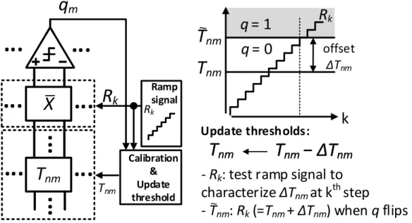
~nm ~Figure 3.6: The foreground calibration process to compensate for bit-cell variations.
3.4
Retraining with Foreground Calibration
Figure 3.6 shows the foreground calibration process to reduce weak classifier errors due to process variations. The foreground calibration uses in-memory comparisons to estimate the offset ∆Tnm between ideal Tnm and realized
˜
Tnm caused by PVT variations in bit-cells and comparators. By comparing
ramp signal Rk and off-chip trained thresholds (Tnm), the update Tnm ← Tnm + ∆Tnm is performed and stored in the BCA to compensate for the
variations. By doing so, foreground calibration achieves 1.3×better memory density than [13] without requiring dedicated offset cancellation bit-cells and 25× lower retraining dataset complexity than [12].
CHAPTER 4
MEASUREMENT RESULTS
This chapter provides the measured results from the prototype IC [11] includ-ing energy, delay, and accuracy. By comparinclud-ing component- and task-level accuracy, DIMA-based AdaBoost architecture demonstrates its robustness to circuit non-idealities and its trade-off between energy and accuracy. The prototype IC from [11] with measurement setup is shown in Fig. 4.1 and its summary is presented in Table 4.1.
4.1
Component-level Accuracy
Figure 4.2 shows the distribution of measured classification results using first and second weak classifiers in 3 vs. 5 strong classifier with different bit-line voltage swing ∆VBL per-LSB. Blue and red dots represent the measured
classification results that are positive and negative, respectively. The black vertical and horizontal lines are used to mark individual ideal thresholds for the first and second weak classifiers. In Fig. 4.2, the classification distribu-tion with lower ∆Vlsb = 15 mV shows more imprecise behaviors than the
classification with higher ∆Vlsb = 25 mV because of higher SNR.
Figure 4.3 shows the measured comparator error rate induced by circuit non-idealities at different BL voltage swings per-LSB for two configurations:
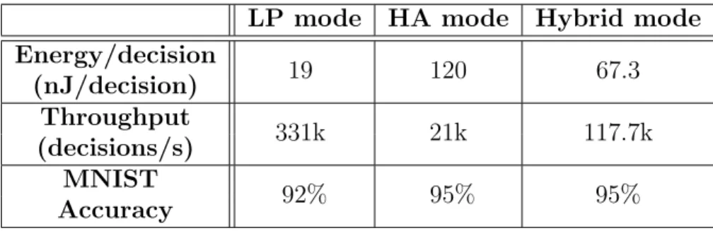
Table 4.1: Measurement summary (∆Vlsb = 30 mV)
LP mode HA mode Hybrid mode
Energy/decision 19 120 67.3 (nJ/decision) Throughput 331k 21k 117.7k (decisions/s) MNIST 92% 95% 95% Accuracy
1. 2 mm 1.2 mm q Bit-cell Array MR -W L d ri ve r& P u ls e ge n . Bit-cell Array MR -W L d ri ver & P u ls e g en . MR -W L d ri ver & P u ls e g en . Normal Read/Write 64 -b b u s
Replica bitcell array Analog comparators
Input buffer &
Cross bar
D ig it al C TRL Test block Base station (Host PC) Prototype PCB Microcontroller module board q[1:128] Technology 65nmCMOS Die size 1.2mm 1.2mm SRAM capacity 16kB Bit-cell dimension 2.11 2.11 CTRL Frequency 1GHz Supply voltage 1V
(a)
(b)
Figure 4.2: Measured results (◦: q = 0, •: q = 1) of the first and second weak classifiers at: (a) ∆Vlsb = 25 mV, and (b) ∆Vlsb = 15 mV, where each
Comparator without calibration Comparator with calibration HA mode without calibration HA mode with calibration
2.7x↓
Figure 4.3: Measured results with (without) foreground calibration: comparator error rate vs. misclassification rate w.r.t. ∆Vlsb for MNIST
dataset.
with and without foreground calibration. The comparison-level errors are measured at each ∆Vlsb [1] by counting the errors during the classification
with MNIST dataset. As the ∆Vlsb increases, the comparator errors reduce
from 50% (53%) to 0.7% (2.5%) with (without) foreground calibration. As shown in Fig. 4.3, the foreground calibration dramatically improves task-level misclassification rate by 21% at ∆Vlsb= 15 mV. In other words, the optimal
operating point can be pushed to the limit where energy efficiency increases at the same level of misclassification rate.
4.2
Task-level Accuracy and Energy
Figure 4.4 shows the misclassification rate for the 10-class MNIST hand-written digit recognition task [19]. As benchmark, we compare with a digital architecture with an identically sized SRAM array and a synthesized digital processor. The energy of the conventional architecture is obtained by mea-suring the SRAM read energy from the prototype IC [11] and the energy
2.6% LP mode with foreground calibration
HA mode with foreground calibration HA mode
LP mode
Figure 4.4: Measurement results: error rate vs. ∆Vlsb for HA mode and LP
mode.
of the digital processor from post-layout simulations. The energy and delay costs of off-chip processing in our architecture are estimated from post-layout simulations. The robustness of classification accuracy to circuit nonidealities is observed as the BL swing ∆Vlsb is reduced. Measurements (Fig. 4.5) show
92% (95%) accuracy in the LP (HA) mode at throughput of 331k (21k) de-cisions/s and energy-efficiency of 19 (120) nJ/decision. This corresponds to 14.7× (7.3×) lower EDP in the LP (HA) mode compared to a conventional digital implementation. In the hybrid mode (Fig. 4.6), 9.70×EDP reduction at accuracy of 95%, energy consumption of 67.3 nJ/decision, and through-put of 117.7K are achieved at Th = 2. In addition, the hybrid mode enables
roughly 26× EDP scalability. Figure 4.7 provides a comparison with recent works that use the MNIST dataset. The proposed in-memory AdaBoost
re-floating point (92%)
LP mode
HA mode
floating point (95%)
LP mode with foreground calibration HA mode with foreground calibration HA mode
LP mode
Figure 4.5: Misclassification rate vs. energy in HA mode and LP mode. alization achieves a 43× reduction in EDP at an iso-accuracy of 95% over a digital neural network [18]. This is a 5% improvement in accuracy over the previous in-memory AdaBoost implementation [13] though at a higher EDP. The higher EDP of our implementation is primarily due to the lower row-parallelism in [11] which reduces the throughput. Furthermore, the proposed architecture can provide energy vs. accuracy scalability by simply adjusting the margin threshold Th as shown in Fig. 4.7. Note that one of the
mea-surement points in [18] is used for iso-accuracy comparison. The comparison graph (Fig. 4.7) also indicates that hybrid mode provides a better EDP point (Th = 2.0) than HA mode at the same accuracy.
C1: (energy), (accuracy) C2: (energy), (accuracy)
Figure 4.6: Error rate vs. average energy in hybrid mode in two configurations: C1=[∆Vlsb(LP) = 15 mV; ∆Vlsb(HP) = 30 mV] and C2=[∆Vlsb(LP) = 30 mV; ∆Vlsb(HP) = 30 mV]. HA mode (8b, 8b) (1-6b, 3-4b) Hybrid mode (5b, 1b)
(input precision, weight precision)
(8b, 8b) (8b, 4-14b) (2b, 3-4b) 43X 5% LP mode Th = 2.0 Th = 0.3 Th = 0.05
Figure 4.7: Accuracy vs. EDP for 10-class MNIST dataset. Throughput and energy scaled to a 65 nm process [13, 17, 18, 20, 21].
CHAPTER 5
CONCLUSION AND FUTURE WORK
5.1
Conclusion
This work presents a hierarchical AdaBoost in-memory classifier to provide scalable architecture in the trade-off between energy and accuracy. As a result, the prototype IC demonstrates that the hybrid mode shows EDP re-duction of 9.70× (95% accuracy) at energy consumption of 67.3 nJ/decision, compared to a conventional digital architecture for MNIST dataset. Also, this work shows 43×reduction of EDP in the same accuracy and 5% improve-ment of accuracy at a similar level of EDP. Foreground calibration compen-sates for the circuit non-idealities of DIMA, achieving task-level accuracy improvement of 21%.
To summarize, there are two crucial points based on the prototype IC mea-surements. First, a scalable architecture by cascading two different modes achieves high accuracy of the HA mode (95%) and low energy consumption (67.3 nJ/decision) that lies between that of the HA and LP modes. Second, foreground calibration helps maximally utilize benefits of mixed-signal com-putations in terms of delay and energy without accuracy loss at low retraining cost, showing EDP reduction of 43×compared to the state-of-the-art digital architecture.
5.2
Future Work
Alternative high-density memory technologies such as NAND flash and MRAM can replace SRAM in this work. As the proposed AdaBoost architecture has a simple structure, resource-constrained applications like IoT devices can employ the proposed design to sustain the always-on functionality. Another
extension to on-chip foreground calibration IC can also be considered to achieve higher robustness under severe resource constraints.
REFERENCES
[1] M. Kang, S. K. Gonugondla, A. Patil, and N. R. Shanbhag, “A multi-functional in-memory inference processor using a standard 6T SRAM array,” IEEE Journal of Solid-State Circuits, vol. 53, no. 2, pp. 642– 655, 2018.
[2] J. Von Neumann, “Probabilistic logics and the synthesis of reliable or-ganisms from unreliable components,” Automata Studies, vol. 34, pp. 43–98, 1956.
[3] M. Horowitz, “Computing’s energy problem (and what we can do about it),” inSolid-State Circuits Conference Digest of Technical Papers (ISSCC), 2014 IEEE International. IEEE, 2014, pp. 10–14.
[4] Y.-H. Chen, T. Krishna, J. S. Emer, and V. Sze, “Eyeriss: An energy-efficient reconfigurable accelerator for deep convolutional neural net-works,”IEEE Journal of Solid-State Circuits, vol. 52, no. 1, pp. 127–138, 2017.
[5] T. Chen, Z. Du, N. Sun, J. Wang, C. Wu, Y. Chen, and O. Temam, “Diannao: A small-footprint high-throughput accelerator for ubiquitous machine-learning,” in ACM Sigplan Notices, vol. 49, no. 4. ACM, 2014, pp. 269–284.
[6] D. Shin, J. Lee, J. Lee, and H.-J. Yoo, “DNPU: An 8.1 TOPS/W re-configurable CNN-RNN processor for general-purpose deep neural net-works,” in Solid-State Circuits Conference (ISSCC), 2017 IEEE Inter-national. IEEE, 2017, pp. 240–241.
[7] B. Moons, R. Uytterhoeven, W. Dehaene, and M. Verhelst, “EN-VISION: A 0.26-to-10 TOPS/W subword-parallel dynamic-voltage-accuracy-frequency-scalable convolutional neural network processor in 28nm FDSOI,” in 2017 IEEE International Solid-State Circuits Conference-(ISSCC) Digest of Technical Papers, 2017, pp. 246–247.
[8] F. Akopyan, J. Sawada, A. Cassidy, R. Alvarez-Icaza, J. Arthur, P. Merolla, N. Imam, Y. Nakamura, P. Datta, G.-J. Nam et al., “Truenorth: Design and tool flow of a 65 mW 1 million neuron programmable neurosynaptic chip,” IEEE Transactions on Computer-Aided Design of Integrated Circuits and Systems, vol. 34, no. 10, pp. 1537–1557, 2015.
[9] N. P. Jouppi, C. Young, N. Patil, D. Patterson, G. Agrawal, R. Bajwa, S. Bates, S. Bhatia, N. Boden, A. Borchers et al., “In-datacenter perfor-mance analysis of a tensor processing unit,” in Computer Architecture (ISCA), 2017 ACM/IEEE 44th Annual International Symposium on. IEEE, 2017, pp. 1–12.
[10] H. Kaul, M. A. Anders, S. K. Mathew, G. Chen, S. K. Satpathy, S. K. Hsu, A. Agarwal, and R. K. Krishnamurthy, “A 21.5 M-query-vectors/s 3.37 nJ/vector reconfigurable k-nearest-neighbor accelerator with adap-tive precision in 14nm tri-gate CMOS,” in IEEE International Solid-State Circuits Conference-(ISSCC) Digest of Technical Papers, 2016, pp. 260–261.
[11] M. Kang, S. K. Gonugondla, S. Lim, and N. R. Shanbhag, “A 19.4 nJ/decision, 364K decisions/s, memory random forest multi-class in-ference accelerator,” IEEE Journal of Solid-State Circuits, no. 99, pp. 1–10, 2018.
[12] S. K. Gonugondla, M. Kang, and N. R. Shanbhag, “A variation-tolerant in-memory machine learning classifier via on-chip training,”IEEE Jour-nal of Solid-State Circuits, no. 99, pp. 1–11, 2018.
[13] J. Zhang, Z. Wang, and N. Verma, “In-memory computation of a machine-learning classifier in a standard 6T SRAM array,” IEEE Jour-nal of Solid-State Circuits, vol. 52, no. 4, pp. 915–924, 2017.
[14] A. Biswas and A. P. Chandrakasan, “Conv-RAM: An energy-efficient SRAM with embedded convolution computation for low-power CNN-based machine learning applications,” in Solid-State Circuits Conference-(ISSCC), 2018 IEEE International. IEEE, 2018, pp. 488– 490.
[15] R. E. Schapire and Y. Freund, Boosting: Foundations and Algorithms. MIT Press, 2012.
[16] Y. Tang, J. Zhang, and N. Verma, “Scaling up in-memory-computing classifiers via boosted feature subsets in banked architectures,” IEEE Transactions on Circuits and Systems II: Express Briefs, 2018.
[17] B. Moons and M. Verhelst, “A 0.3–2.6 TOPS/W precision-scalable pro-cessor for real-time large-scale ConvNets,” in VLSI Circuits (VLSI-Circuits), 2016 IEEE Symposium on. IEEE, 2016, pp. 1–2.
[18] P. N. Whatmough, S. K. Lee, H. Lee, S. Rama, D. Brooks, and G.-Y. Wei, “A 28nm SoC with a 1.2GHz 568nJ/prediction sparse deep-neural-network engine with >0.1 timing error rate tolerance for IoT applications,” in Solid-State Circuits Conference (ISSCC), 2017 IEEE International. IEEE, 2017, pp. 242–243.
[19] Y. LeCun and C. Cortes, “MNIST handwritten digit database,” 2010, AT&T Labs. [Online]. Available: http://yann.lecun.com/exdb/mnist [20] J. K. Kim, P. Knag, T. Chen, and Z. Zhang, “A 640m pixel/s 3.65 mW
sparse event-driven neuromorphic object recognition processor with on-chip learning,” in VLSI Circuits (VLSI Circuits), 2015 Symposium on. IEEE, 2015, pp. C50–C51.
[21] F. N. Buhler, P. Brown, J. Li, T. Chen, Z. Zhang, and M. P. Flynn, “A 3.43 TOPS/W 48.9 pJ/pixel 50.1 nJ/classification 512 analog neuron sparse coding neural network with on-chip learning and classification in 40nm CMOS,” in VLSI Circuits, 2017 Symposium on. IEEE, 2017, pp. C30–C31.

![Figure 2.1: Proposed in-memory computing hardware: (a) DIMA [1, 11], and (b) data-flow.](https://thumb-us.123doks.com/thumbv2/123dok_us/9724974.2854049/15.918.165.679.192.432/figure-proposed-memory-computing-hardware-dima-data-flow.webp)