Ahmed, K.H. and Adam, G.P. and Abdelsalam, I. and Aboushady, A.A.
(2018) Modular multilevel converter with modified half-bridge submodule
and arm filter for DC transmission systems with DC fault blocking
capability. IET Power Electronics. ISSN 1755-4535 (In Press) ,
This version is available at
https://strathprints.strath.ac.uk/65088/
Strathprints is designed to allow users to access the research output of the University of Strathclyde. Unless otherwise explicitly stated on the manuscript, Copyright © and Moral Rights for the papers on this site are retained by the individual authors and/or other copyright owners. Please check the manuscript for details of any other licences that may have been applied. You may not engage in further distribution of the material for any profitmaking activities or any commercial gain. You may freely distribute both the url (https://strathprints.strath.ac.uk/) and the content of this paper for research or private study, educational, or not-for-profit purposes without prior permission or charge.
Any correspondence concerning this service should be sent to the Strathprints administrator: [email protected]
The Strathprints institutional repository (https://strathprints.strath.ac.uk) is a digital archive of University of Strathclyde research outputs. It has been developed to disseminate open access research outputs, expose data about those outputs, and enable the
1
Modular Multilevel Converter with Modified Half-Bridge Submodule and Arm
Filter for DC Transmission Systems with DC Fault Blocking Capability
K.H. Ahmed
1, G.P. Adam
1, I. Abdelsalam
2, A.A. Aboushady31 Department of Electronics and Electrical Engineering, Faculty of Engineering, University of Strathclyde, 204 George Street, Glasgow, UK
2 Electrical and Control Department, College of Engineering and Technology, Arab Academy for Science, Technology and Maritime Transport, Cairo, Egypt
3 School of Engineering and Built Environment, Glasgow Caledonian University, 70 Cowcaddens Road, Glasgow, UK
*corresponding author: [email protected]
Abstract:Although a modular multilevel converter (MMC) is universally accepted as a suitable converter topology for the high voltage dc transmission systems, its dc fault ride performance requires substantial improvement in order to be used in critical infrastructures such as transnational multi-terminal dc (MTDC) networks. Therefore, this paper proposes a modified submodule circuit for modular multilevel converter that offers an improved dc fault ride through performance with reduced semiconductor losses and enhanced control flexibility compared to that achievable with full-bridge submodules. The use of the proposed submodules allows MMC to retain its modularity; with semiconductor loss similar to that of the mixed submodules MMC, but higher than that of the half-bridge submodules. Besides dc fault blocking, the proposed submodule offers the possibility of controlling ac current in-feed during pole-to-pole dc short circuit fault, and this makes such submodule increasingly attractive and useful for continued operation of MTDC networks during dc faults. The aforesaid attributes are validated using simulations performed in MATLAB/SIMULINK, and substantiated experimentally using the proposed submodule topology on a 4-level small-scale MMC prototype.
1. Introduction
At present the voltage source converter high voltage direct current (VSC-HVDC) transmission system offers a number of attractive features, which are well suited for multi-terminal dc grids [1-2]. Some of its attractive features for generic dc grids are: active or dc power reversal being achieved without change of DC link voltage polarity; resilience to ac side network faults without risk of commutation failure as with the line commutating counterpart. However, vulnerability of VSC-HVDC transmission systems to dc faults and absence of cost-effective fast acting dc circuit breakers capable of operating at high voltage restrict their applications to point-to-point connection [3-7].
With emergence of modular multilevel converter (MMC) in early 2000s as an attractive alternative to conventional two-level and active neutral-point clamped converters for high voltage applications [8-10], voltage source converters have drawn significant research interests from industry and academia. Modular multilevel converter provides a viable way to construct a high quality stepped approximation of sinusoidal ac voltage from large number of discrete voltage levels provided by submodule capacitors. Full-scale MMC with hundreds of submodules per arm presents a nearly perfect sinusoidal ac voltage to interfacing transformer, with approximately zero total harmonic distortion and extremely low-voltage gradient (dv/dt) [10]. However, the MMC, compared to conventional two-level converter, has some weaknesses such as its large semiconductor footprint and its energy storage which is nearly tenfold of the two-level converter of similar rating. This results in slow dynamic response compared to two-level converter. Since its conception, half-bridge (HB) and
full-bridge (FB) submodules have received significant attention as they allow maximum modularity of the MMC
power circuit, internal fault management, mass
manufacturing, maintenance and ease of transportation. Half-bridge modular multilevel converter (HB-MMC) presents lower number of semiconductor switches in conduction path compared to the full-bridge modular multilevel converter (FB-MMC); thus, it has lower semiconductor losses [12]. Both HB-MMC and FB-MMC can operate continuously under unbalanced conditions and survive symmetrical and asymmetrical ac network faults (ac fault ride-through). Although the use of distributed submodule capacitors in HB-MMC improves its response to dc fault, its freewheeling diodes remain vulnerable to excessive current stresses and high di/dt during dc short circuit fault. FB-MMC offers dc fault blocking capability plus additional features such as operation with reduced dc voltage, which is critical for dc pole voltage restraining during pole-to-ground dc fault; and operation with positive and negative dc link voltages, which is vital in generic dc grids [11-12]. Unfortunately, all such attributes are superseded by the high cost of the HVDC converters and high switching/conduction losses. Therefore, major manufacturers have found difficulties in convincing utilities to adopt typical FB-MMC. In recent years, mixed submodule MMC (also known as optimised full-bridge MMC) has been presented as an alternative to typical FB-MMC, with even split between the HB and FB submodules. This corresponds to the minimum number of FB submodules needed to offer dc fault blocking, without exposing submodule capacitors and switching devices to excessive voltage stresses [13]. Generally, the number of HB and FB submodules in mixed submodule MMC could be selected to deliver custom features [14]. However, the use of
2 two types of submodules may lead to limited compromise to
modularity of the power circuit and increase the complexity of the modulation and control.
Apart from HB and FB submodules, there are several submodule configurations presented in [15-18] such as double clamped and three-level submodules that offer no additional benefits beyond that of the FB-MMC or mixed submodule MMC. Therefore, they are less likely to be adopted in practical systems due to the entanglements of these submodules, which have wider implications on the modularity of the power circuit, and in facilitation of continued operation during internal faults.
Other converter topologies that offer dc fault blocking are an alternative arm modular multilevel converter and a hybrid cascaded two-level converter with ac-side or dc-side full-bridge submodules [13, 19-20]. These types of converters are developed intentionally to optimise or lower converter footprint and conversion losses compared to the FB-MMC, but their modularity are compromised by the use of series connected IGBTs in the main power stage. At the present time, there are two competing approaches for multi-terminal dc grids and for clearing dc faults. The first approach is to use HB-MMC with fast acting dc circuit breakers to isolate dc faults within few milliseconds from fault initiation. But development of such fast dc circuit breaker is still in its early stages. A prototype of hybrid dc circuit breaker that can break dc current of up to 9kA within 2ms was tested at 80-kVdc [21], and this is far from today’s VSC-HVDC transmission systems dc operating voltage, which is up to 640 kV pole to pole, and with power handling capacity of 1 GW. The second approach is to use reverse blocking converters that can extinguish the fault current in semiconductor switches instantly [22-27], allowing the fault current in the dc side to decay; thus, the fault can be cleared using low-cost disconnectors. Some converters such FB-MMC and mixed submodule FB-MMC offer an additional feature of extinguishing the fault current in the dc side instantly by providing counter voltage (brief reverse of dc link voltage). However, the main weakness of the latter approach is that it relies on complete collapse of the dc voltage, and this means the power exchange between converters connected to the affected dc grid would drop to zero during converter blocking and fault clearance period. Both of the above approaches for fault clearance are valid but the choice between them must be made on case by case, considering the merits and demerits of each approach.
This paper presents a modified submodule for the MMC that operates in similar manner to conventional HB submodule during normal operation and offers complete dc fault blocking. The proposed submodule offers dc fault blocking at a similar level of semiconductor losses as the minimum possible from mixed submodules MMC, but with much lower semiconductor footprint. Operational and control principles of the proposed submodule are explained in detail. It is also demonstrated that the MMC employing the proposed submodules can operate with reduced dc link voltage and survive dc fault without converter blocking and risk of damage. This is because the proposed submodule allows some level of controllability over ac current in-feed during dc fault. Such feature is attractive for continued operation of multi-terminal HVDC networks. The viability of this promising submodule is confirmed using simulations performed in MATLAB/SIMULINK and corroborated
experimentally on scaled down prototype of 4-level MMC with 3 submodules per arm.
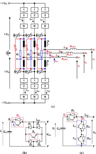
2. System configuration
Fig. 1 (a) shows a generic MMC. Submodules in the upper and lower arms of generic MMC can be replaced by any of the proposed configurations in Fig. 1 parts (b) and (c) for dc fault blocking capability. Notice that type 1 (Fig. 1 (b)) and type 2 (Fig. 1(c)) topologies use similar structure as the conventional HB submodule, except that the lead switch Sa is replaced by a composite switch with a bidirectional blocking capability. Types 1 and 2 topologies generate two
voltage levels between ‘X’ and ‘Y’, Vsm=0 and Vsm=VC;
where VC represents submodule capacitor voltage. They
generate voltage level Vsm=0 when their composite lead
switches Sa are turned on and auxiliary switches Sx are turned off. When the current direction for the proposed submodule is assumed to be positive, the current conduction paths for type 1 and 2 topologies are summarised in Table 1 and Table 2, respectively. The main advantage of type 1 is using one gate driver per lead switch instead of two compared to type 2. However, Table I shows that the type 1 submodule inserts two diodes and one IGBT in conduction path when synthesizing voltage level Vsm=0; thus, increases
the semiconductor losses of the MMC that employs type 1 submodule. For this reason, type 1 submodule will be abandoned in favour of type 2 submodule which more efficient as it inserts one diode and one IGBT in conduction path for both arm current polarity when the submodule capacitor is being bypassed. Therefore, type 1 submodule will not be investigated further in this paper; instead, the focus will be only on type 2 submodule. Type 2 submodule inserts only one semiconductor switch (diode or IGBT) into conduction path when generating voltage level Vsm=VC as in
conventional HB submodule. From the above discussions, it can be concluded that the MMC that uses type 2 topology presents the same number of semiconductor switches in conduction path per phase as mixed submodules MMC when 50% of its submodules are of FB type.
Table 1 Summary of current conduction paths of type 1 submodule and their influence on the capacitor voltage
Voltage level
Polarity of arm
current ( Iarm) Current path
Capacitor voltage (Vc) Vsm= 0 IIarm> 0 D1SaD4 Unchanged arm< 0 D2SaD3 Vsm= Vc Iarm> 0 Freewheeling diode of composite switch Sx(Dx) Charge Iarm< 0 IGBT of composite switch S
x(Tx) Discharge
Table 2 Summary of current conduction paths of type 2 submodule and their influence on the capacitor voltage
Voltage level
Polarity of arm
current ( Iarm) Current path
Capacitor voltage (Vc) Vsm= 0 IIarm> 0 Ta1Da2 Unchanged arm< 0 Ta2Da1 Vsm= Vc Iarm> 0 Freewheeling diode of composite switch Sx(Dx) Charge Iarm< 0 IGBT of composite switch S
3
(a)
(b) (c)
Fig. 1. (a) Modular multilevel converter with proposed submodules (b) Proposed Type 1 submodule (c) Proposed Type 2 submodule.
3. Proposed protection against overvoltage
As in FB submodules, the proposed submodule achieves dc fault blocking (stops ac grid contribution to dc fault) by inhibiting the gating signals to the converter switches. However, the main drawback of the proposed submodule is that there are no conduction paths when arm currents are negative at the instant of converter blocking. This may create significant overvoltage in converter arms, which may destroy semiconductor switches [28]. The main countermeasure adopted in this paper is the use of high-pass RC filters across the arm inductors to provide path for the upper and lower arm currents at instant of converter blocking. Fig. 2 parts a and b present illustration of conduction paths in MMCs with FB submodule and proposed type 2 submodule when gating signals are inhibited, using one phase leg, with red arm currents refer to positive direction and blue arm currents refer to negative
direction. When phase ‘a’ upper arm current (ia1) is negative,
the arm current cannot flow through any of the proposed submodules as each submodule inserts at least one revered biased diode in conduction path. Therefore, the only viable conduction path will be through the high impedance path being provided by the high-pass RC filter that intends to dissipate the stored energy in the arm inductors in the resistance of the RC filter and with any excessive energy due to overvoltage will be absorbed by the surge arrestor. To
minimize the loss in the RC branch at power frequency range, the parameters of the high-pass filter (HPF) must be selected such that the RC branch presents high impedance at frequencies below 200Hz, while allowing high frequency currents at the instant of blocking to be diverted to the RC branch, see frequency response in Fig. 3. Recall that the
HPF cut-off frequency ( c) is , where, RF and
CF are filter resistance and capacitance. The impendence at
fundamental frequency is 2 2 2
0 F 1 0 F
Z R C , and when the
filter cut-off frequency is expressed as multiple fundamental frequency as cn0, the filter impedance at fundamental
frequency could be approximated by 2
0 F 1
Z R n . The
maximum current flow through the RC filter depends on the clamping voltage (Vclamp) of the surge arrester (50kV is
assumed in this paper), and dominant frequency of the oscillatory arm current that would be diverted to the RC branch at the instant of the IGBT blocking. For example, with RF=1.6kΩ and CF=285nF, n= c/ 0≈7, which indicates
Z0≈11.3kΩ (high enough to suppress fundamental current in
the HPF to near zero; hence minimizes the steady-state losses). The maximum current in the RC branch
is 2
1
2clamp F res F
V R C , where res is the frequency of the
resonance that may arise during converter blocking.
(a) (b)
Fig. 2. Illustration of blocking state (a) full-bridge MMC (b) MMC with type 2 submodule.
0 50 100 150 200 250 300 350 400 0 10 20 30 40 50 f(Hz) Z (K il o O hm )
Fig. 3. Frequency response of the RC branch
4. Modulation and control strategies
In this paper, the nearest level modulation is used and
Marquardt’s capacitor voltage balancing technique is
4 Fig. 4. Generic control system employed to control the proposed MMC
4.1. Control Structure
The proposed control allows regulation of the submodule capacitor voltages to be coupled to the input dc link voltage by maintaining the dc component of the insertion function (
m
d
1
N V V
dc c , Vdc is the dc linkvoltage,
V
c is the average submodule capacitor voltage)fixed at unity (md= 1) as shown in Fig. 4. From the basic
definition of md, this makes the submodule capacitor
voltages to follow the input dc link voltage as it varies
according to 1
c dc
V NV . The main attribute of this method is that it does not expose converter switching devices to extra current stresses as long as the minimum dc link voltage remains above the peak line-to-line voltage imposed by the interfacing transformer at the converter terminals. However, the main drawback of this method is that the converter active and reactive powers exchanges with the ac network become increasingly coupled to the dc link voltage.
4.2. System Equations
Based on phase ‘a’ current polarities in Fig. 1(a), the differential-mode current represents converter output phase ac current (ia) and is given by:
a a1 a 2
i
i
i
(1)where ia1 andia2 are the currents flowing in the upper and
lower arms respectively.
Similarly, the common-mode current that represents the shared or circulating current component between the upper and lower arms is:
1
cir 2 a1 a 2
i
( i
i )
(2)The instantaneous voltages developed across the submodule of the upper (positive) and lower (negative) arms of phase
‘a’ va1(t), and va2(t) are:
1
( )
( ) ,
2( )
( )
a a a u c a l cv t
t V v t
t V
(3) where 12(
sin(
))
a uN m m
dt
, 12(
sin(
))
a lN m m
dt
Using KVL, the MMC internal dynamics due to fundamental and circulating currents can be expressed as:
1 1 1 2 2 2
(
)
cir d d cir dc a adi
L
R i
V
v
v
dt
(4) 1 1 1 1 2 2 2 2(
)
a d d a a a aodi
L
R i
v
v
v
dt
(5)After transforming three-phase version of (4 and 5) into d-q synchronous reference frame, where the d-axis aligned with
phase ‘a’ of the grid voltage, the following equations are obtained: 1 1 1 1 2 2 2 2 1 1 1 1 2 2 2 2 ( ) ( ) ( ) cos ( ) ( ) ( ) sin d T d T d d T d q c q T d T d q T d d c di L L R R i L L i mV dt di L L R R i L L i mV dt (6) Based on (6), the inner current controller that regulates the fundamental current in synchronous reference frame is designed using similar procedures as described in [27, 30]; while the circulating current controller is designed using similar procedures described in [11].
5. Performance evaluation
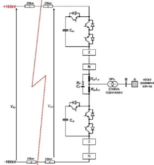
This section utilises MMC that employs 22 proposed submodules per arm to illustrate its steady-state and transient response to reduced dc voltage operation and dc network faults as shown in Fig. 5. The system parameters are listed in Table 3.
5.1. Reduced dc Voltage Operation
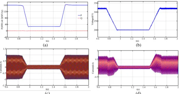
This subsection aims to demonstrate a reduced dc voltage operation of the MMC that employs the proposed submodule. The dc link voltage (Vdc) is initially set at rated
(320kV) and converter is commanded to inject 160 MW at unity power factor into the ac grid (G) at the point of common coupling B. At time t=0.75s; the dc link voltage is reduced gradually from 320kV to 200kV, then at t=1.5s, the dc link voltage is returned back gradually to 320kV. Fig 6(a) shows that although the active power command is constant, the injected active power into the ac grid reduces with the dc link voltage (Fig. 6(b)). Notice that any reduction in
5 converter dc link voltage will be associated with reduction
of fundamental converter voltage (Vcm= ½mVdc) at converter
terminal; therefore, converter control would act immediately to increase modulation index in attempt to keep constant output active power by increasing Id. In the case of large
reduction in dc link voltage, converter control system would increase the modulation index to its upper limit, and control over active power will be temporary lost, leading to noticeable reduction in converter active power output as depicted in Fig. 6(a). Fig. 6 parts (c) and (d) show converter three-phase output currents and sample of phase ‘a’ upper and lower arm currents. Fig. 7(a) shows that the submodule capacitor voltages follow the dc link voltage when dc component of the modulation functions is kept fixed at 1. When comparing the plots for the voltage developed across the upper and lower arms of phase (va1 and va2) during
steady-state operation at rated dc link voltage (320kV) to that at reduced dc link voltage (200kV) as shown in Fig. 7 parts (b) and (c), it can be noticed that the (va1 and va2) in the
latter case are clamped due to modulation index saturation. Line-to-line ac voltage waveform in Fig. 7(d) shows that the converter output voltage is not significantly distorted when its residual dc link voltage remains above the critical voltage (peak of line-to-line voltage), even though its modulation index available for voltage control is saturated to maximum limit. Additional scenario (reduction of dc link voltage to 25% of the rated voltage) is simulated to present that the proposed MMC would not result in large and uncontrolled ac current in-feed from the ac grid as in the HB-MMC. In this case, reduction of the dc link voltage is initiated at t=0.75s and command for dc voltage restoration to rated dc voltage is given at t=1.8s, and the rest of system operating conditions remain as in the previous case. Fig. 8 shows that although the dc link voltage falls below the peak line voltage, the proposed submodule allows the converter to retain some degree of controllability over active and reactive powers. This is because the lead switches in the proposed submodules remain fully controllable despite the fall of the converter dc link voltage to lower than the peak of the line-to-line ac voltages at converter terminal. Notice that the loss of controllability over the active power as the converter is unable to synthesize the interfacing transformer fundamental voltage at its terminals when the modulation index is saturated. This results in limited over-current in the ac side and in the converter upper and lower arms as shown in Fig. 8 parts (c) and (d). The plot for the submodule capacitor voltages displayed in Fig. 9(a) shows that the capacitor voltages follow the dc link voltage. Fig. 9 parts (b) and (c)
show voltage developed across phase ‘a’ upper and lower
arm voltages and their zoomed version during reduced dc link operation. The above discussions show that the proposed MMC experience limited overcurrent during collapse of dc link voltage, and this feature is attractive for continued operation of multi-terminal HVDC networks using low cost mechanical dc circuit breakers and small size dc decoupling inductors compared to that in [31].
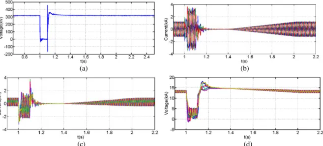
5.2. Response to dc Network fault 5.2.1. Without Converter Blocking
This subsection examines the proposed MMC ride through dc fault capability, without converter blocking (pre-fault conditions remains the same as in previous subsection). The test network in Fig. 5 is subjected to solid pole-to-pole
dc fault at t= 1s, with 100ms duration. When the fault is detected, converter output active power is reduced to zero immediately and the power transfer is resumed gradually by ramping up converter output active power at t=1.4s (300ms from the fault clearance). Fig. 10 parts (a), (b) and (c) show converter dc link voltage, three-phase output currents and upper and lower arm currents. Observe that although the dc link voltage has collapsed compared to peak of the phase voltage, the current stresses in the converter switches remain within acceptable limits. The submodule capacitor voltages are shown in Fig. 10(d).
5.2.2. With Converter Blocking
This subsection illustrates the dc reverse blocking of the MMC with the proposed type 2 submodules, assuming the same pre-fault operating conditions as previous subsections.
Fig. 5. Proposed test system of HVDC link that employs MMC with the proposed submodules.
Table 3 Test system parameters
Converter rated parameters Values
DC link voltage 320kV
Active power rating 200 MW
Reactive power rating 60MVAr
submodule capacitance 1.25mF (43.6ms)
Arm inductor 25mH
Number of submodule per arm 22
Nominal submodule capacitor voltage 14.55kV
AC System Parameters
AC grid voltage 400kV
AC grid three-phase short circuit level 20000MVA
AC grid X/R 16
AC grid frequency 50 Hz
Interfacing transformer rated parameters
Interfacing transformer rated power 210MVA Interfacing transformer voltage ratio 400kV/132kV Interfacing transformer leakage reactance 20%
DC line parameters
DC cable length 50km
DC cable resistance 1.27mΩ/km
DC cable inductance 0.93mH/km
DC cable capacitance 0.095µF/km
High-pass filter resistance (RF) 1.6kΩ
6 A temporary solid pole-to-pole dc short circuit is applied at
t=1s, converter blocking is activated after 50µs from fault inception, fault is cleared at t=1.1s, converter is de-blocked at t=1.2s, and power transfer is resumed at t=1.4s by ramping the converter output power gradually from zero to pre-fault condition (160MW at unity power factor). Fig. 11 parts (a), (b) and (c) show converter dc link voltage, three-phase output currents and upper and lower arm currents. Observe that converter blocking is sufficient to force the currents in the converter switches to zero; thus, eliminating the risk of switches failure due to grid contribution. The plots of the submodule capacitor voltages are in Fig. 11(e). It is obvious that the proposed MMC is able to block dc fault, without exposing converter arms to excessive voltage stresses. Fig. 12(a) shows the RC branch current. It can be seen that the RC branch draws negligible current during steady-state operation and provides path for the current at
converter blocking. Fig. 12(b) shows with snubber resistance and capacitance in Table 3, the worst-case transient power loss per RC branch at fault inception and clearance, which it is about 150kW per phase leg.
6. System comparison
Results of analytical semiconductor loss comparison for MMCs with half-bridge, full-bridge, double submodules and the proposed submodules are shown in Table 4, considering two operating points, and assuming 4.5kV IGBTs (T1800GB45A) and 50% device utilization (2.25kV per device). The analytical loss estimations of the MMCs that employ the proposed submodules are verified using simulation results. See that the MMC with type 2 submodule has similar semiconductor loss as that of the MMCs with mixed submodules or three-level double clamped submodules. Additionally, the costs comparison presented in (a) (b)
(c) (d)
Fig. 6. Simulation results at reduced dc link voltage operation; (a) Active and reactive power converter exchanges, (b) DC link voltage, (c) Converter three-phase output currents, and (d) Sample of the upper and lower arm currents (phase a).
(a) (b)
(c) (d)
Fig. 7. Simulation results at reduced dc link voltage operation; (a) Submodule capacitor voltages, (b) Snapshot of voltages va1 and va2, when dc link voltage is reduced to 200kV, (c) Snapshot of the voltages va1 and va2 when dc link voltage is at rated, 320kV, and (d) line-to-line ac voltage at converter terminal superimposed on dc link voltage measured during reduced dc voltage operation.
7 Table 5 is calculated based on the practical approach
described in [32]. Table 5 shows that the approximate semiconductor cost of the MMC with the proposed cell is practically the same as the mixed cell MMC, and with both appear to offer marginally lower costs than that of the MMC with double clamped cell. This is because the double clamped cell uses additional blocking diodes.
It is worth mentioning that during simultaneous energization of the submodule capacitors and dc circuit, a small auxiliary dc power supply should be embedded in each submodule to turn on the switch Ta2 only during start-up then the power
will be supplied via the submodule capacitors as normal.
(a) (b)
(c) (d)
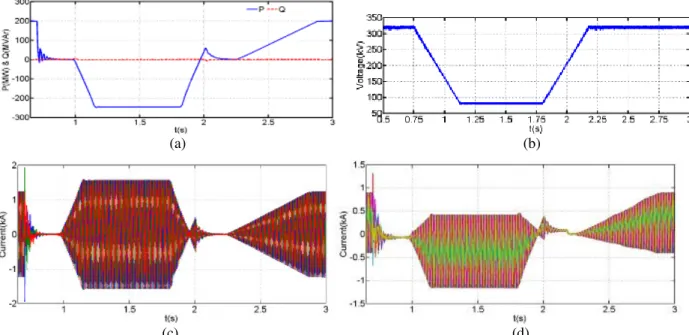
Fig. 8. Simulation results at reduced dc link voltage (to 25% of its rated voltage); (a) Active and reactive power converter exchanges, (b) DC link voltage, (c) Converter three-phase output currents, and(d) Phase ‘a’ upper and lower arm currents.
(a) (b)
(c) (d)
Fig. 9. Simulation results at reduced dc link voltage (to 25% of its rated voltage); (a) Submodule capacitor voltages, (b) Voltage waveforms developed across submodules of the upper and lower arms of phase a, (c) Snapshot of voltage waveforms developed across submodules of the upper and lower arms of phase a, zoomed during reduced dc link voltage, and (d) Converter line-to-line ac terminal voltage superimposed on the its dc link voltage.
8 (a) (b)
(c) (d)
Fig. 10. Simulation results at pole-to-pole dc short circuit fault without converter blocking (a) DC link voltage (b) Converter three-phase output currents, (c) Upper and lower arm currents of the three phases, (d) Submodule capacitor voltages.
(a) (b)
(c) (d)
Fig. 11. Simulation results at dc reverse blocking of the converter; (a) DC link voltage (b) Converter three-phase output currents, (c) Upper and lower arm currents of the three phases, (d) Submodule capacitor voltages.
0.980 1 1.02 1.04 1.06 1.08 1.1 1.12 1.14 1.16 0.05 0.1 0.15 t(s) P (M W ) (a) (b)
Fig. 12. Simulation results at dc reverse blocking of the converter; (a) Current in the RC branch across phase ‘a’ arm reactors, and (b) Power dissipation in the high-pass filter branch across the upper and lower arm inductors.
9 Table 4 Modular multilevel converter topologies
comparison (320kV dc link voltage, 209MVA converter, with rated active and reactive powers of 200MW and ±60MVAr, rated ac voltage interfacing transformer imposes
at converter terminal is 132kV, switching devices’
parameters are: VT0=1.82V, VD0=2.27V, rT=1.2mΩ and
rD=1.07mΩ).
Table 5 Cost comparison with modular multilevel converter topologies (320kV dc link voltage, 209MVA converter, 4.5kV IGBTs (T1800GB45A) and 50% device utilization (2.25kV per device))
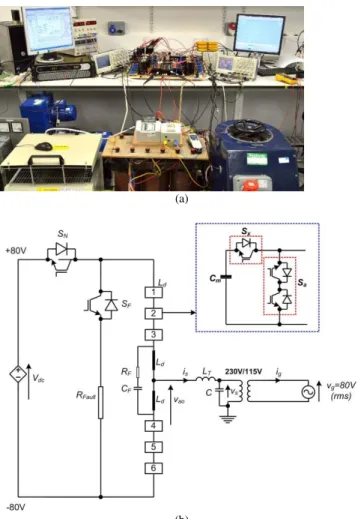
7. Experimental results
This section uses low power rated single-phase prototype of the proposed MMC with three submodules per arm as shown in Fig. 13(a). Modulation, capacitor voltage balancing algorithm and proposed control system were implemented via a 32-bit Cypress microcontroller (CY8CKIT-050 PSoC® 5LP). Due to low number of submodules per arms, a pulse width modulation with relatively high switching frequency of 2kHz is adopted. MMC submodule capacitance and arm inductance are 2.2mF and 3mH, and dc link voltage is fixed at 160V during normal operation and emulated dc faults, with and without converter blocking. Fig. 13(b) displays schematic diagram of the prototype of the proposed converter, where ac side filter inductance LT=1mH and capacitance C=20µF. Two
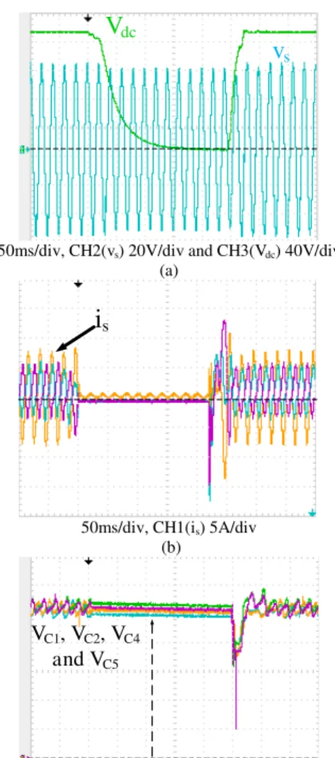
experimental scenarios considered in this section are simulated pole-to-pole dc fault without and with converter blocking. Fig. 14 shows experimental waveforms obtained when the proposed converter is subjected to simulated pole-to-pole dc fault, with duration of 250ms. In pre-fault condition, the converter is fed from a programmable dc power supply, with Vdc= 160V, switches SN and SF are on
and off respectively. The temporary fault is initiated by commanding the dc power supply to reduced its dc output voltage (Vdc) from 160V to 53V ( ×160V), and switch SF is
turned on to connect the bleeding resistance (RFault=12Ω)
across the dc link in order to consume the active power that may flow from the ac grid toward the dc side during the
period when (½Vdc) is lower than the peak of the phase ac
voltage at converter terminal. The fault clearance instant is simulated by disconnection of bleeding resistance (RFault)
and fast increase of the Vdc to 160V. Fig. 14(a) displays the
dc link voltage (Vdc) superimposed on the phase ac voltage
(vs) measured at the low-voltage side of the interfacing
transformer. Fig. 14 parts (b) and (c) present converter output phase current, and its associated upper and lower arm currents respectively. Observe that although the dc link voltage has collapsed compared to peak of the phase voltage (Vm> > ½Vdc), the current stresses in the converter switches
remain within tolerable limits, and the capacitor voltage balancing method is able to keep the submodule capacitor voltages to follow the dc link voltage. These results are in line with the simulation results presented in section V.
(a)
(b)
Fig. 13. Experimental test rig: (a) Prototype of the proposed MMC, and (b) schematic diagram of the prototype. In addition, it can see be seen that during fault ride through without converter blocking, the residual dc link voltage and submodule capacitor voltages become insufficient to synthesize the ac voltage imposed at converter terminal by the interfacing transformer, and these have resulted in noticeable distortions in the converter output voltage. Fig. 15 presents experimental waveforms of the proposed converter during simulated pole-to-pole dc fault and converter blocking is activated. Fig. 15(a) shows dc link voltage (Vdc) superimposed on the phase voltage (vs). Fig. 15
parts (b) and (c) present output phase current (is) measured
at low-voltage side of the interfacing transformer, and superimposed on the upper and lower arm currents. Observe
Converter type On-state losses P=200MW and Q=0 P=200MW and Q=60MVAr MMC with mixed submodules 1.46MW
(0.703%) 1.45MW (0.693%) MMC with half-bridge submodules 0.91MW (0.437%) 0.96MW (0.462%) MMC with full-bridge submodules 1.82MW (0.874%) 1.93MW (0.924%) MMC with 3-level submodules
(double clamped) 1.46MW (0.703%) 1.45MW (0.693%) MMC with type-2 submodules analytical 1.46MW (0.703%) 1.45MW (0.693%) simulation 1.44MW (0.689%) 1.41MW (0.673%)
Converter type Cost (£/kVA)
MMC with mixed submodules 148
MMC with half-bridge submodules 99
MMC with full-bridge submodules 198 MMC with 3-level submodules (double clamped) 173 MMC with proposed type-2 submodules 148
10 that the proposed converter has stopped grid contribution to
dc fault as the arm currents and output phase current drop to zero as converter blocking is activated. The traces for the submodule capacitor voltages displayed in Fig. 15(d) remain unchanged during converter blocking as expected, and exhibit short curation voltage dip due to brief period of mismatch between residual submodule capacitor voltages at the instant of converter blocking and Vdc/N at the instant of
converter de-blocking. These experimental results support the simulation results of the proposed converter.
8. Conclusion
This paper proposed a modified half bridge submodule circuit that could be used to improve dc fault survival of modular multilevel converter. Operating principle of the proposed submodule was explained, including control
structure. The viability of the proposed submodule was verified using simulations performed on MATLAB- SIMULINK environment, considering dc fault ride through of one terminal of the VSC-HVDC that employs MMC with 22 submodules per arm. The validity of the presented simulation results was validated by experimental results obtained from small scale prototype of single-phase MMC that employs 3 submodules per arms. The presented simulation and experimental results indicate that the MMC which uses the proposed submodule can ride through dc faults with and without converter blocking. These are achieved while producing less semiconductor losses than FB-MMC and comparable with mixed submodules MMC, but with lower semiconductor area compared to mixed submodules MMC. Hence the proposed submodule enjoys all favourable features from the other submodule topologies. The particular merit of riding through dc faults without converter blocking makes the MMC that employs the proposed submodule a frontline candidate for cost-effective MTDC networks that employ relative cheap and slow dc
V
dcvs
50ms/div, CH2(vs) 20V/div and CH3(Vdc) 40V/div
(a)
50ms/div, CH1(is) 5A/div, CH2(ia1) 5A/div, and CH3(ia2) 5A/div
(b) VC1, VC2, VC4
and VC5
50ms/div, CH1(VC1) 10V/div, CH2(VC2) 10V/div, CH3(VC4) 10V/div,
and CH4(VC5) 10V/div
(c)
Fig. 14. Experimental waveforms during simulated pole-to-pole dc fault, without considering converter
blocking: (a) Converter dc link voltage (Vdc)
superimposed on output phase voltage (vs) measured at
low-voltage side of the interfacing transformer, (b) Output phase current measured at low-voltage side of the interfacing transformer, and (c) Submodule capacitor voltages.
V
dcvs
50ms/div, CH2(vs) 20V/div and CH3(Vdc) 40V/div
(a)
is
50ms/div, CH1(is) 5A/div
(b)
VC1, VC2, VC4
and VC5
50ms/div, CH1(VC1) 10V/div, CH2(VC2) 10V/div, CH3(VC4) 10V/div,
and CH4(VC5) 10V/div
(c)
Fig. 15. Experimental results at pole-to-pole dc fault (converter blocking): (a) Converter dc link voltage (Vdc)
superimposed on the phase voltage (vs), (b) Output phase
current (is) superimposed on the upper and lower arm
currents (ia1 and ia2), and (c) Samples of submodule
11 circuit breakers (especially as it has been demonstrated that
the converter switches are not exposed to excessive current stresses beyond that can be tolerated by commercial IGBTs).
9. References
[1] G. P. Adam, K. H. Ahmed, S. J. Finney, K. Bell and B. W. Williams, "New Breed of Network Fault-Tolerant Voltage-Source-Converter HVDC Transmission System," Power Systems, IEEE Transactions on, vol. 28, pp. 335-346, 2013. [2] G. P. Adam, I. A. Abdelsalam, K. H. Ahmed and B. W. Williams, "Hybrid Multilevel Converter with Cascaded H-bridge Cells for HVDC Applications: Operating Principle and Scalability," IEEE Transactions on Power Electronics, vol. 30, pp. 65-77, 2015.Applications: Operating Principle and Scalability," IEEE Transactions on Power Electronics, vol. 30, pp. 65-77, 2015.
[3] C. M. Franck, "HVDC Circuit Breakers: A Review Identifying Future Research Needs," IEEE Transactions on Power Delivery, vol. 26, pp. 998-1007, 2011.
[4] W. Yeqi and R. Marquardt, "Future HVDC-grids employing modular multilevel converters and hybrid DC-breakers," in Power Electronics and Applications (EPE), 2013 15th European Conference on, 2013, pp. 1-8.
[5] C. C. Davidson, et al., "A new ultra-fast HVDC Circuit breaker for meshed DC networks," in AC and DC Power Transmission, 11th IET International Conference on, 2015, pp. 1-7.
[6] B. C. Kim, et al., "Development of HVDC circuit breaker with fast interruption speed," in 2015 9th International Conference on Power Electronics and ECCE Asia (ICPE-ECCE Asia), 2015, pp. 2844-2848.
[7] C. Oates, "Modular Multilevel Converter Design for VSC HVDC Applications," IEEE Journal of Emerging and Selected Topics in Power Electronics, vol. 3, pp. 505-515, 2015. [8] E. Solas, G. Abad, J. A. Barrena, S. Aurtenetxea, A. Carcar, and L. Zajac, "Modular Multilevel Converter With Different Submodule Concepts—Part II: Experimental Validation and Comparison for HVDC Application," Industrial Electronics, IEEE Transactions on, vol. 60, pp. 4536-4545, 2013.
[9] Q. Song, W. Liu, X. Li, H. Rao, S. Xu, and L. Li, "A Steady-State Analysis Method for a Modular Multilevel Converter," IEEE Transactions on Power Electronics, vol. 28, pp. 3702-3713, 2013.
[10] G. Minyuan and X. Zheng, "Modeling and Control of a Modular Multilevel Converter-Based HVDC System under Unbalanced Grid Conditions," Power Electronics, IEEE Transactions on, vol. 27, pp. 4858-4867, 2012.
[11] G. P. Adam and I. E. Davidson, "Robust and Generic Control of Full-Bridge Modular Multilevel Converter High-Voltage DC Transmission Systems," Power Delivery, IEEE Transactions on, vol. 30, pp. 2468-2476, 2015.
[12] C. Chao, G. P. Adam, S. Finney, J. Fletcher and B. Williams, "H-bridge modular multi-level converter: control strategy for improved DC fault ride-through capability without converter blocking," Power Electronics, IET, vol. 8, pp. 1996-2008, 2015.
[13] G. P. Adam, K. H. Ahmed and B. W. Williams, "Mixed cells modular multilevel converter," in Industrial Electronics (ISIE), 2014 IEEE 23rd International Symposium on, 2014, pp. 1390-1395.
[14] G. P. Adam, S. J. Finney and B. W. Williams, "Enhanced control strategy of full-bridge modular multilevel converter," in 2015 International Conference on Renewable Energy Research and Applications (ICRERA), 2015, pp. 1432-1436.
[15] V. Dargahi, A. K. Sadigh, M. Abarzadeh, S. Eskandari and K. A. Corzine, "A New Family of Modular Multilevel Converter Based on Modified Flying-Capacitor Multicell Converters," Power Electronics, IEEE Transactions on, vol. 30, pp. 138-147, 2015.
[16] A. Nami, L. Jiaqi, F. Dijkhuizen and G. D. Demetriades, "Modular Multilevel Converters for HVDC Applications: Review on Converter Cells and Functionalities," Power Electronics, IEEE Transactions on, vol. 30, pp. 18-36, 2015. [17] J. Qin, M. Saeedifard, A. Rockhill and R. Zhou, "Hybrid Design of Modular Multilevel Converters for HVDC Systems Based on Various Submodule Circuits," IEEE Transactions on Power Delivery, vol. 30, pp. 385-394, 2015.
[18] J. Zhang and C. Zhao, "The Research of SM Topology with DC Fault Tolerance in MMC-HVDC," IEEE Transactions on Power Delivery, vol. 30, pp. 1561-1568, 2015.
[19] R. Zeng, L. Xu, L. Yao and D. J. Morrow, "Precharging and DC Fault Ride-Through of Hybrid MMC-Based HVDC Systems," IEEE Transactions on Power Delivery, vol. 30, pp. 1298-1306, 2015.
[20] R. Li, J. E. Fletcher, L. Xu, D. Holliday and B. W. Williams, "A Hybrid Modular Multilevel Converter With Novel Three-Level Cells for DC Fault Blocking Capability," IEEE Transactions on Power Delivery, vol. 30, pp. 2017-2026, 2015.
[21] J. HÄFNER; and B. JACOBSON, "Proactive Hybrid HVDC Breakers - A key innovation for reliable HVDC grids," presented at the Cigre 2011, The Electric Power System of the Future-Integrating Supergrids and Microgrids International Symposium, BOLOGNA, 2011.
[22] S. Debnath, Q. Jiangchao, B. Bahrani, M. Saeedifard and P. Barbosa, "Operation, Control, and Applications of the Modular Multilevel Converter: A Review," Power Electronics, IEEE Transactions on, vol. 30, pp. 37-53, 2015.
[23] G. P. Adam, I. A. Gowaid, S. J. Finney, D. Holliday and B. W. Williams, "Review of dc-dc converters for multi-terminal HVDC transmission networks," IET Power Electronics, vol. 9, pp. 281-296, 2016.
[24] S. Cui and S. K. Sul, "A Comprehensive DC Short Circuit Fault Ride Through Strategy of Hybrid Modular Multilevel Converters (MMCs) for Overhead Line Transmission," IEEE Transactions on Power Electronics, vol. PP, pp. 1-1, 2016. [25] F. Deng, Y. Tian, R. Zhu and Z. Chen, "Fault-Tolerant Approach for Modular Multilevel Converters Under Submodule Faults," IEEE Transactions on Industrial Electronics, vol. PP, pp. 1-1, 2016.
[26] G. Liu, F. Xu, Z. Xu, Z. Zhang and G. Tang, "Assembly HVDC Breaker for HVDC Grids with Modular Multilevel Converters," IEEE Transactions on Power Electronics, vol. PP, pp. 1-1, 2016.
[27] R. Oliveira and A. Yazdani, "A Modular Multilevel Converter with DC Fault Handling Capability and Enhanced Efficiency for HVDC System Applications," IEEE Transactions on Power Electronics, vol. PP, pp. 1-1, 2016.
[28] K. H. Ahmed and A. A. Aboushady, "Modified half-bridge modular multilevel converter for HVDC systems with DC fault ride-through capability," in IECON 2014 - 40th Annual Conference of the IEEE Industrial Electronics Society, 2014, pp. 4676-4682.
[29] B. Jacobson, P. Karlsson, G. Asplund, L. Harnnart, and A. T. Jonsson, "VSC-HVDC Transmission with Cascaded Two-level Converters," presented at the CIGRE 2010, 2010.
[30] G. P. Adam and B. W. Williams, "Half- and Full-Bridge Modular Multilevel Converter Models for Simulations of Full-Scale HVDC Links and Multiterminal DC Grids," IEEE Journal
12 of Emerging and Selected Topics in Power Electronics, vol. 2,
pp. 1089-1108, 2014.
[31] G. P. Adam, R. Li, D. Holliday, S. Finney, L. Xu, B. W. Williams, K. T. Uda, M. S. Kuroda, R. Yamamoto, and H. Ito, "Continued Operation of Multi-Terminal HVDC Networks Based on Modular Multilevel Converters," presented at the Cigre, Lund, 2015.
[32] S. P. Engel, M. Stieneker, N. Soltau, S. Rabiee, H. Stagge, and R. W. De Doncker, "Comparison of the modular multilevel dc converter and the dual-active bridge converter for power conversion in hvdc and mvdc grids," IEEE Transactions on Power Electronics, vol. 30, no. 1, pp. 124–137, 2015.