Sn-Ag Based Solders Bonded to Ni-P/Au Plating:
Effects of Interfacial Structure on Joint Strength
Tomoyuki Hiramori
1;*, Mototaka Ito
2, Yoshiharu Tanii
2, Akio Hirose
1and Kojiro F. Kobayashi
11
Department of Manufacturing Science, Graduate School of Engineering, Osaka University, Suita 565-0871, Japan 2Surface Science Labs, Toray Research Center. Inc, Otsu 520-8567, Japan
This study investigates interfacial reaction and joint strength of Sn-Ag and Sn-Ag-Cu solder balls bonded to electroless Ni-P plating with various thicknesses of Au coating (50, 250 and 500 nm). For the Sn-Ag solder joints, a P-rich layer formed after reflow-soldering at the joint interface, regardless of thickness of the Au coating. However, for the Sn-Ag-Cu solder joints, a P-rich layer formed at the joint interface only in those samples with Au coating of 250 and 500 nm. Fractures were found to occur at the interface, and the joint strength degraded at Au thickness
of>250nm for both the Sn-Ag and Sn-Ag-Cu solder joints. An Au thickness of 50 nm resulted in the best joint strength.
(Received July 18, 2003; Accepted September 26, 2003)
Keywords: Lead free solder, electroless Ni-P/Au plating, ball grid array, interfacial reaction, joint strength
1. Introduction
The development of lead-free solders for use in the micro-soldering of electronic devices is important because the eutectic Sn-Pb solder, which is commonly used, is environ-mentally harmful and can potentially affect human health. The most attractive alternatives to the eutectic Sn-Pb solder are the Sn-Ag based solders. However, those solders have disadvantages due to their high melting points and poor wettability compared with the eutectic Sn-Pb solder. In order to lower the melting point and improve the mechanical properties of the Sn-Ag solder, a third element such as Cu or Bi must be added. In addition, to improve wettability, Au-coated electroless Ni-P plating on Cu land can be applied to the soldering. When the Ni-P plating is applied however, the solder joint degrades due to a brittle intermetallic compound layer and/or a P-rich layer that forms on the solder and Ni-P plating interface.1)Moreover, it has been reported that a thick Au coating may decrease joint reliability.2) However, the effect of the thickness of Au coatings has not yet been tested. In this paper, a Sn-Ag solder ball or a Sn-Ag-Cu solder for BGA (Ball Grid Array) was reflow-soldered on the Cu land coated with Au of various thicknesses on electroless Ni-P plating. The metallographic observation of the solder joints after the reflow and subsequent aging treatment were performed using scanning electron microscope (SEM) and auger electron spectroscopy (AES). Joint strength measure-ments were performed using cold and hot bump pull tests. Fracture surfaces were observed using SEM following the tests. Based on the results, the influence of the Au coating thickness on the interfacial structure and on the joint strength was evaluated and discussed.
2. Experimental Procedure
In this study, four types of substrates consisting of Cu pads coated with Ni-P including about 10 mass%P/Au platings with Au thicknesses of 50, 250 and 500 nm were used. The
diameter of the pad was 500mm. A Sn-3.5Ag (mass%) solder ball and a Sn-3.5Ag-0.75Cu (mass%) solder ball of 700mm
diameter were used for BGA.
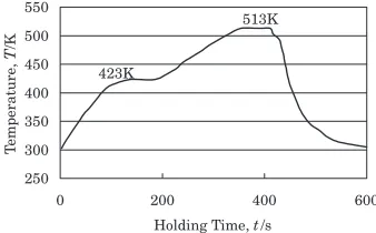
The reflow conditions included a peak reflow temperature of 513 K for 60 s with preheating at 423 K for 60 s as shown in Fig. 1. The solder balls were reflow-soldered onto the Cu pads using a rosin type flux in air. After the reflow-soldering, some of the samples were aged at 423 K for 0.72 to
3:6106s in air.
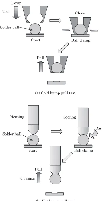
After the reflow-soldering and aging treatments, a cold bump pull test and a hot bump pull test were performed to measure the joint strength of each sample using a bond tester (DAGE Inc., DAGE-SERIES-4000P). Figure 2 schemati-cally illustrates the cold and hot bump pull tests. A speed of 300mm/s was used in both tests. In the hot bump pull test, the probe was coated with Sn-Pb plating to improve wettability of the probe to the solder ball. Prior to the test, it was confirmed that the interface structure was not affected by the dissolution of Pb during the test.
After the reflow-soldering and aging treatments, the cross-sectional microstructure at the interface between the solder and pad was observed using SEM and TEM (Transmission Electron Microscopy). The chemical composition of the reaction products was then analyzed using AES. The reaction products were identified based on AES quantitative analysis. The cross section and the fracture surface of the samples were observed after the cold and hot bump pull tests.
250 300 350 400 450 500 550
0 200 400 600
Holding Time, t/s
T
emperature,
T
/K
513K
423K
Fig. 1 Reflow thermal profile.
*Graduate Student, Osaka University
[image:1.595.341.510.662.767.2]3. Results and Discussion
3.1 Microstructure of interface
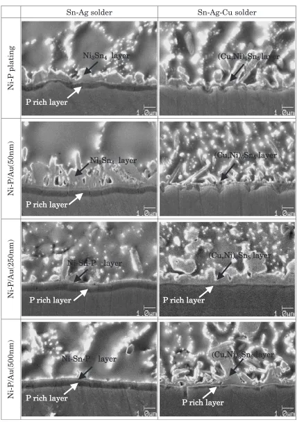
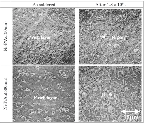
Figure 3 presents SEM images of the interfacial micro-structure of the Sn-Ag solder and Sn-Ag-Cu solder joints following reflow-soldering. In the Sn-Ag solder joints, a Ni3Sn4layer formed on the interface of the samples without
Au coating and those with a 50 nm Au coating. No obvious Ni3Sn4layer formed in the interface of the samples with 250
and 500 nm Au coating. The AES line analysis across the interface of the sample with a 500 nm Au coating was preformed, and the results are shown in Fig. 4. Although Ni3Sn4partly formed at the interface, it was discontinuous. A
thin Ni-Sn-P layer formed continuously on the interface. When Sn-Ag solder was used, regardless of thickness of the Au coating, a P-rich layer formed on the interface.3,4)Figure 5 shows a TEM image of the interfacial microstructure in the Sn-Ag solder joint sample, with 500 nm Au coating. A P-rich layer having a fibrous structure formed of the Ni-P plating and a Ni-Sn-P layer having a polycrystalline structure was seen between the P-rich layer and solder layer. A sequence of micro-voids was clearly observed in the Ni-Sn-P layer. Such structure at the Sn-Ag solder and Ni-P plating interface has been reported also from other researchers. The micro-voids sequence may have an detrimental effect on joint strength at interface.5–7)Difference in the interfacial structures resulting from the thickness of the Au coating was noted in the as reflowed samples, and it was therefore considered that the
thickness of the Au coating may affect the interfacial reaction during the reflow process.8)
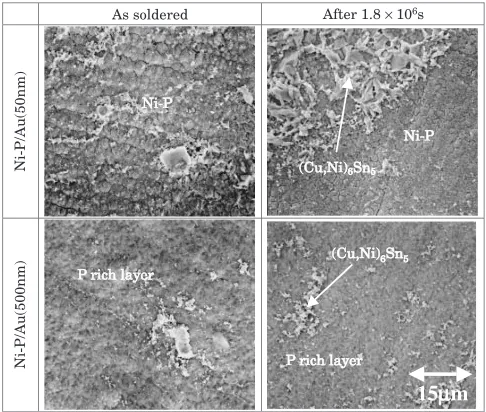
In the Sn-Ag-Cu solder joints, a (Cu,Ni)6Sn5layer formed
on the interface, regardless of thickness of the Au coating. Formation of a obvious P-rich layer on the interface was not observed. In the (Cu,Ni)6Sn5 layer, Ni content is
approx-imately 18%, which is significantly lower than in the Ni3Sn4
layer. Therefore, in the Sn-Ag-Cu solder joints, the amount of Ni diffusion from the Ni-P plating to the solder was significantly lower than in the Sn-Ag solder joints. This is thought to occur because the (Cu,Ni)6Sn5 layer acts as a
barrier layer, suppressing the diffusion of Ni from the electroless Ni-P plating to the solder layer.9)However, in the samples with 250 and 500 nm Au coating, a thin P-rich layer was observed at the interface. This indicates that even using the Sn-Ag-Cu solder, a thick Au coating (>250nm) causes the formation of a P-rich layer on the interface after reflow-soldering.
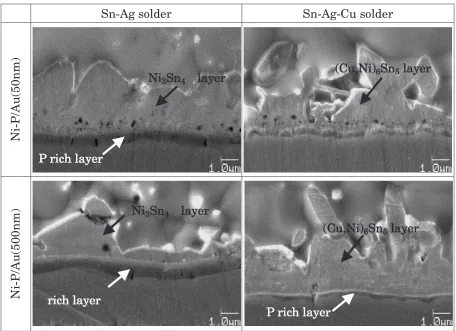
Figure 6 shows SEM images of the interfacial micro-structure in the Sn-Ag solder, and the Sn-Ag-Cu solder joints after aging treatment at 423 K for1:8106s. Following the
aging treatment, a Ni3Sn4layer as well as a P-rich layer grew
on the Sn-Ag solder. This finding suggests that Ni from the electroless Ni-P plating diffused into the solder layer during the aging treatment.
The (Cu,Ni)6Sn5 layer also grew on the Sn-Ag-Cu solder
during the aging treatment. No P-rich layer formed on the interface following the aging treatment for those samples without Au (and those with 50 nm Au coating), that had no P-rich layer in the interface after the reflow-soldering. No apparent growth of the P-rich layer was observed in those samples with 250 and 500 nm Au coatings that had a thin P-rich layer in the interface after the reflow-soldering. These results indicate that the diffusion of Ni from the electroless Ni-P plating to the solder layer was suppressed by the barrier effect of the (Cu,Ni)6Sn5 layer during the aging treatment.
Thus, adding Cu to the Sn-Ag solder effectively suppresses the diffusion of Ni from the electroless Ni-P plating to the solder layer by forming a stable (Cu,Ni)6Sn5 layer at the
interface.
Figure 7 plots the reaction layer thickness and the P-rich layer thickness as a function of the square root of the aging time at 423 K for the Sn-Ag and Sn-Ag-Cu solder joints without Au coating and with 50 and 500 nm Au coating. In the samples without Au coating and with 500 nm Au coating, the Ni3Sn4layer thickness increased exponentially during the
aging treatment. However, in the Sn-Ag solder, the growth of the Ni3Sn4 layer in the sample with 50 nm Au coating was
slower and was not parabolic. As shown in Fig. 3, in the sample with 50 nm Au coating, the Ni3Sn4layer after
reflow-soldering appeared needle-like and skeleton morphology, while that in the sample without Au coating was monolithic layer and the sample with 500 nm Au coating had no obvious Ni3Sn4layer. During the aging treatment, in the sample with
50 nm Au coating, Ni that diffused to the solder layer from the Ni-P plating can react Sn existing in the gaps between the Ni3Sn4 needles to form Ni3Sn4. While this changed the
skeleton Ni3Sn4layer to the monolithic one (Figs. 3 and 6),
the growth of the Ni3Sn4 layer toward the solder layer was
suppressed. Regardless of the Au coating thickness, the
(a) Cold bump pull test
(b) Hot bump pull test Down
Tool
Solder ball
Start
Close
Ball clamp
Pull
Heating
Solder ball
Cooling
Air
Ball clamp
Start
Pull
0.3mm/s
Fig. 2 Schematic illustrations of (a) cold bump pull test and (b) hot bump
[image:2.595.83.252.72.405.2]thickness of the P-rich layer increased up to a holding time of
0:72106s. Thereafter, no changes in the thickness of the P-rich layer were observed. The results indicate that when Sn-Ag solder is used, Au coating thickness affects not only the interface structure after the reflow-soldering but also the growth behavior of the reaction layer during the aging treatment.
When the Sn-Ag-Cu solder was used, the (Cu,Ni)6Sn5
reaction layer thickness increased monotonically during the aging treatment, independent of the Au coating thickness. As a result, it was found that Au coating thickness has little effect on the growth behavior of the (Cu,Ni)6Sn5 reaction
layer during the aging treatment. Moreover, during the aging treatment, no changes were detected in the P-rich layer
Sn-Ag solder
Sn-Ag-Cu solder
Ni-P
plating
Ni-P/Au(50nm)
Ni-P/Au(250nm)
Ni-P/Au(500nm)
Ni
Ni
3Sn
Sn
4layer
layer
P rich layer
P rich layer
Ni
Ni
3Sn
Sn
4layer
layer
P rich layer
P rich layer
Ni-Sn-P
Ni-Sn-P
layer
layer
P rich layer
P rich layer
Ni-Sn-P
Ni-Sn-P
layer
layer
P rich layer
P rich layer
P rich layer
P rich layer
P rich layer
P rich layer
(Cu,Ni)
(Cu,Ni)
6Sn
Sn
5layer
layer
(Cu,Ni)
(Cu,Ni)
6Sn
Sn
5layer
layer
(Cu,Ni)
(Cu,Ni)
6Sn
Sn
5layer
layer
(
Cu,Ni)
Cu,Ni)
6Sn
Sn
5layer
layer
[image:3.595.83.511.65.673.2]0 20 40 60 80 100
0 4
Distance, d/ µm
Atomic concentration (%)
Ni
Ni
3Sn
Sn
4Sn Sn
P P Ni Ni
2 6 8
Fig. 4 SEM image and AES line profile of the interface between the solder
and the Ni-P plating with 500 nm Au coating.
500nm
P-rich layer Ni-Sn-P layer Solder
micro-void sequence
Ni-P plating
Fig. 5 TEM image of the Sn-Ag solder joint with 500 nm Au coating.
Sn-Ag solder
Sn-Ag-Cu solder
Ni-P/Au(50nm)
Ni-P/Au(500nm)
Ni
Ni
3Sn
Sn
4layer
layer
P rich layer
P rich layer
(Cu,Ni)
(Cu,Ni)
6Sn
Sn
5layer
layer
Ni
Ni
3Sn
Sn
4layer
layer
P rich layer
P rich layer
(Cu,Ni)
(Cu,Ni)
6Sn
Sn
5layer
layer
rich layer
rich layer
Fig. 6 SEM images of the Sn-Ag solder and the Sn-Ag-Cu solder using various thicknesses of Au plating after heat treatment for
[image:4.595.50.291.73.365.2] [image:4.595.307.547.167.313.2] [image:4.595.70.526.426.757.2]thickness of the sample with 500 nm Au coating, in which the P-rich layer formed at the interface after the reflow-soldering. In the sample with 50 nm Au coating thickness, a P-rich layer was not observed, even after a holding time of 3:6106s. This suggests that differences in the Au coating thickness in the Sn-Ag-Cu solder joints can affect the interfacial reaction primarily during the reflow-soldering, not in aging treatment.
3.2 Joint strength 3.2.1 Cold bump pull test
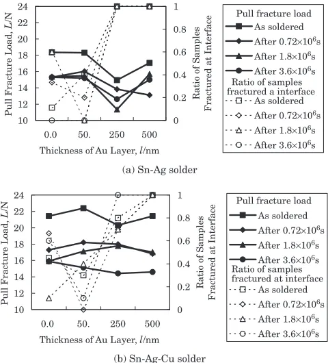
The cold bump pull test was performed on the Sn-Ag and Sn-Ag-Cu solder joints following the aging treatment. Figure 8 presents the test results and ratio of samples that were fractured at the interface. This ratio was calculated as number of samples fractured at the interface region between the solder and the land, divided by the total number of samples measured. Details of the fracture positions in the interfacial region will be discussed in the following section. In the solder joints, strength decreased following the aging treatment, regardless of the Au coating thickness. Fractures
occurred mainly in the solder layer for the samples without Au coating or with 50 nm Au coating. For the samples with 250 and 500 nm Au coating, fractures occurred at the interface. When tensile stress is applied to a component consisting of serially bonded multiple materials, a fracture occurs in a material or at a bonding interface of which strength is the lowest. Since the strength of the interface can be higher than that of the solder layer in the samples that were fractured in the solder layer. Thus the test results suggest that the bonding strength of the interface reduces with increasing Au coating thickness.
The strength of the Sn-Ag-Cu solder joints was found to be higher than that of the Sn-Ag solder joints after both the reflow-soldering and aging treatments. This result might be caused by the solid solution strengthening of Cu in the samples without Au coating (and those with 50 nm Au coating), where fracturing occurred mainly in the solder layer. In the samples with 250 and 500 nm Au coating, where fractures occurred at the interface, the bonding strength of the interface in the Sn-Ag-Cu solder joints would be expected to be higher than that of the Sn-Ag solder joints. Our results suggest that not only the formation of the P-rich layer, but also its thickness affect the bonding strength of the interface.
3.2.2 Hot bump pull test
Figure 9 depicts the results of the hot bump pull test follwoing the aging treatment. Since fractures occurred at the interface for all of the samples, the bonding strength of the interface can be evaluated directly.
In both the Sn-Ag and Sn-Ag-Cu solder joints, the samples with 50 nm Au coatings had greater strength than those without Au coating. However, in the joints with 250 nm Au coating, the joint strength was reduced. For both the Sn-Ag and Sn-Ag-Cu solder joints, we found that 50 nm Au coating (a) Ni3Sn4 layer
(b) (Cu,Ni)6Sn5 layer
(c) P-rich layer 0 0.5 1 1.5 2 2.5 3 3.5
0 500 1000 1500 2000
Holding Time, t/s1/2
Thickness,
l
/
µ
m
No Au coating 50nm Au coating 500nm Au coating
0 0.5 1 1.5 2 2.5 3 3.5
0 500 1000 1500 2000
Holding Time,t/s1/2
Thickness,
l
/
µ
m
No Au coating 50nm Au coating 500nm Au coating
0 0.1 0.2 0.3 0.4 0.5 0.6 0.7 0.8 0.9 1
0 500 1000 1500 2000
Holding Time, t/s1/2
Thickness, l / µ m Sn-Ag solder/non Au coating Sn-Ag solder/Au(50nm) Sn-Ag solder/Au(500nm) Sn-Ag-Cu solder/Au(500nm)
Fig. 7 The thickness of the reaction layer and the P-rich layer as a function
of aging time.
10 12 14 16 18 20 22 24
0.0 50. 250 500
Thickness of Au Layer, l/nm
Pull Fracture Load,
L /N 0 0.2 0.4 0.6 0.8 1
Ratio of Samples
Fractured at Interface
As soldered After 0.72×10⁶s After 1.8×10⁶s After 3.6×10⁶s
As soldered After 0.72×10⁶s After 1.8×10⁶s After 3.6×10⁶s
(a) Sn-Ag solder
10 12 14 16 18 20 22 24
0.0 50. 250 500
Thickness of Au Layer, l/nm
Pull Fracture Load,
L /N 0 0.2 0.4 0.6 0.8 1
Ratio of Samples
Fractured at Interface
As soldered After 0.72×10⁶s After 1.8×10⁶s After 3.6×10⁶s
As soldered After 0.72×10⁶s After 1.8×10⁶s After 3.6×10⁶s
(b) Sn-Ag-Cu solder
Pull fracture load
Ratio of samples fractured a interface
Pull fracture load
Ratio of samples fractured at interface
Fig. 8 Effect of the thickness of the Au layer on the cold bump pull fracture
[image:5.595.52.291.70.502.2] [image:5.595.307.547.73.338.2]is the optimum coating thickness from the viewpoint of the joint strength.10)
[image:6.595.49.292.72.385.2]3.3 Fracture surface observation results 3.3.1 Cold bump pull test
Figure 10 displays SEM images of the fracture surfaces of the Sn-Ag solder and the Sn-Ag-Cu solder joints with 500 nm Au coating that were fractured at the interface in the cold bump pull test following reflow-soldering and the aging treatment for1:8106s.
In the Sn-Ag solder joint, a P-rich layer was exposed on the fracture surface after reflow-soldering. It is thought that this fracture occurred between the P-rich and Ni-Sn-P layers. However, since the Ni3Sn4phase was frequently observed on
the fracture surface of the samples following the aging treatment for 1:8106s, it is possible that the fractures
occurred between the Ni3Sn4and solder layers in the samples
following the aging treatment.
In the Sn-Ag-Cu solder joint, the fracture surface was located on the Ni-P plating layer, and the (Cu,Ni)6Sn5phase
was partly observed on the fracture surface. It is possible that the fracture occurred between both the Ni-P plating layer and the (Cu,Ni)6Sn5 layer after the reflow-soldering and aging
treatments.
3.3.2 Hot bump pull test
Figures 11 and 12 show the SEM images of the fracture surfaces after the hot bump pull test for the Ag and Sn-Ag-Cu solder joints, respectively. Based on the observations of the fracture surface, the interfacial structure correlating with the fracture mode and joint strength of the Sn-Ag and
Sn-Ag-Cu solder joints are summarized in Tables 1 and 2, respectively. In the Sn-Ag solder sample without Au coating, no P-rich layer was observed on the fracture surface on the pad side after reflow-soldering. The fracture was thought to occur at the interface between the P-rich and Ni-P plating layers. With the Sn-Ag solder samples with Au coating, the P-rich layer was exposed on the fracture surface, regardless of Au coating thickness. The fracture was therefore thought to occur between the P-rich layer and the Ni-Sn-P layer. After the aging treatment for1:8106s, regardless of Au coating thickness, the Ni3Sn4 phase was observed on the fracture
surface. Thus, the fracture was thought to occur between the
(a) Sn-Ag solder
(b) Sn-Ag-Cu solder
10 12 14 16 18 20 22 24 26
0 200 400 600
Thickness of Au Layer, l/nm
Pull Fracture Load,
L
/N
As soldered
After 0.72×10⁶s
After 1.8×10⁶s
After 3.6×10⁶s
10 12 14 16 18 20 22 24 26
0 200 400 600
Thickness of Au Layer, l/nm
Pull Fracture Load,
L
/N
As soldered
After 0.72×10⁶s
After 1.8×10⁶s
After 3.6×10⁶s
Fig. 9 Effect of the thickness of the Au layer on the hot bump pull fracture
strength of (a) the Sn-Ag solder and (b) the Sn-Ag-Cu solder.
As soldered After 1.8 × 10⁶s
Sn-Ag solder
Sn-Ag-Cu solder
15
15
µ
m
m
P rich layerP rich layer
Ni Ni3SnSn4
P
P rich layerrich layer (Cu,Ni)
(Cu,Ni)6SnSn5 P rich layer P rich layer
(Cu,Ni) (Cu,Ni)6SnSn5 Solder
[image:6.595.306.548.72.341.2]Solder
Fig. 10 SEM images of the fracture surface of the Ag solder and the
Sn-Ag-Cu solder after cold bump pull test.
As soldered After 1.8 × 10⁶s
Ni-P/Au(50nm)
Ni-P/Au(500nm)
15
µ
m
P rich layerP rich layer
P rich layer P rich layer
Ni Ni3SnSn4
Ni Ni3SnSn4
Fig. 11 SEM images of the fracture surface of the Sn-Ag solder joint after
[image:6.595.306.548.386.593.2]Ni3Sn4 and Ni-Sn-P layers. Moreover, a greater amount of
Ni3Sn4 phase was observed on the fracture surface in the
sample with thicker Au coating. Thus, the fracture position of the joint after the aging treatment was found to differ from that after the reflow-soldering, when the Sn-Ag solder was used. The growth of the Ni3Sn4 layer during the aging
treatment may cause changes in the fracture position. That is,
it is considered that the Ni3Sn4layer formed during the aging
treatment is brittle and has considerable low strength, and this can promote fracture initiation and propagation when tensile stress is applied.
With the Sn-Ag-Cu solder, since the Ni-P plating was predominantly exposed on the fracture surface when the samples without Au coating and with 50 nm Au coating were used, it is thought that the fracture occurred between the Ni-P plating layer and the (Cu,Ni)6Sn5 layer. There was no
difference between the fracture modes before and after the aging treatment. On the other hand, the fracture occurred between either the Ni-P plating layer and the P-rich layer, or between the P-rich layer and the (Cu,Ni)6Sn5 layer in the
samples with 250 and 500 nm Au coating after the reflow-soldering. The fracture position was almost the same as that observed following the aging treatment. Since the samples with thicker Au coating exhibited lower joint strength, the formation of the P-rich layer seems to reduce bonding strength at the interface.
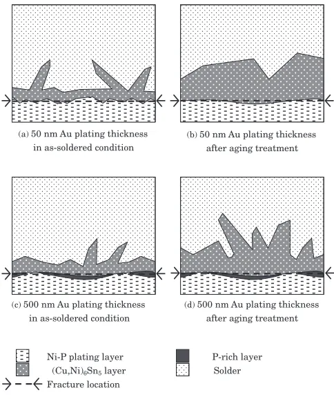
The above considerations are summarized in Fig. 13 and Fig. 14 schematically illustrate the interfacial structures and fracture locations of the Sn-Ag and Sn-Ag-Cu solder joints. With the Sn-Ag solder joints, fractures occurred either between the Ni-P layer and P-rich layer or between the P-rich layer and the Ni-Sn-P layer after the reflow-soldering. Therefore, it is apparent that formation of the P-rich and Ni-Sn-P layers can degrade the joint strength. However, while the fracture location was almost the same regardless of the Au coating thickness, the joint strength of the sample with
As soldered After 1.8 × 10⁶s
Ni-P/Au(50nm)
Ni-P/Au(500nm)
15
µ
m
Ni-PNi-P
P rich layer rich layer
Ni-P Ni-P
(Cu,Ni) (Cu,Ni)6SnSn5
[image:7.595.47.290.73.279.2]P rich layer rich layer (Cu,Ni) (Cu,Ni)6SnSn5
Fig. 12 SEM images of the fracture surface of the Sn-Ag-Cu solder joint
[image:7.595.46.552.450.577.2]after the hot bump pull test.
Table 1 Summary of the interfacial structure and fracture mode of the Sn-Ag solder joint.
Thickness of Au P-rich Interfacial Load
Fracture location
coating (nm) layer reaction layer (N)
0 thick Ni-Sn-P/Ni3Sn4 14.4 Ni-P/P-rich layer
As soldered 50 thick Ni-Sn-P/Ni3Sn4 19.7 P-rich layer/Ni-Sn-P
250 thick Ni-Sn-P 14.0 P-rich layer/Ni-Sn-P
500 thick Ni-Sn-P 14.1 P-rich layer/Ni-Sn-P
0 thick Ni-Sn-P/Ni3Sn4 16.3 Ni-Sn-P/Ni3Sn4
After 50 thick Ni-Sn-P/Ni3Sn4 19.4 Ni-Sn-P/Ni3Sn4
1:8106s 250 thick Ni-Sn-P/Ni
3Sn4 16.1 Ni3Sn4
[image:7.595.48.550.612.786.2]500 thick Ni-Sn-P/Ni3Sn4 15.8 Ni3Sn4
Table 2 Summary of the interfacial structure and fracture mode of the Sn-Ag-Cu solder joint.
Thickness of Au P-rich Interfacial Load
Fracture location
coating (nm) layer reaction layer (N)
0 non (Cu,Ni)6Sn5 18.6 Ni-P/(Cu,Ni)6Sn5
50 non (Cu,Ni)6Sn5 23.8 Ni-P/(Cu,Ni)6Sn5
As soldered 250 thin (Cu,Ni)6Sn5 18.1
P-rich layer
/(Cu,Ni)6Sn5
500 thin (Cu,Ni)6Sn5 17.0
P-rich layer
/(Cu,Ni)6Sn5
0 non (Cu,Ni)6Sn5 10.3 Ni-P/(Cu,Ni)6Sn5
50 non (Cu,Ni)6Sn5 19.2 Ni-P/(Cu,Ni)6Sn5
After
250 thin (Cu,Ni)6Sn5 17.2
P-rich layer
1:8106s /(Cu,Ni)
6Sn5
500 thin (Cu,Ni)6Sn5 16.9
P-rich layer
50 nm Au coating was higher than that of the samples with 250 and 500 nm Au coating. This suggests that formation of the needle-like Ni3Sn4layer at the interface may beneficially
influence the joint strength. After the aging treatment, the fracture position was observed at either the Ni3Sn4 layer or
the interface between the Ni-Sn-P layer and the Ni3Sn4layer
although the joint strength was hardly changed from that in the as-reflowed condition. This suggests that the thick and monolithic Ni3Sn4 layer that formed after the heat treatment
may be more harmful than the P-rich layer for the interfacial structure. Further studies are needed to investigate the effect of the morphology of the Ni3Sn4 phase on the fracture
behavior of the Sn-Ag solder joints.
For the Sn-Ag-Cu solder joints, a comparison between the sample with 50 nm Au coating and the samples with 250 and 500 nm Au coating, following the reflow-soldering and aging treatments, showed that the joint strength of the sample with a 50 nm Au coating was much higher than that of the samples with 250 and 500 nm Au coating. It is therefore thought that the formation of the P-rich layer at the interface degrades the joint strength. Moreover, in the samples without Au coating and with 50 nm Au coating in which no P-rich layer formed at the interface, the latter joint strength was higher than that of the former. Thus, although Au coating of an adequate thickness on the electroless Ni-P plating improves wetablility between the pad and the solder and increases joint strength, excessive Au coating results in the deterioration of joint strength. The results of this study suggest that 50 nm Au coating thickness provides the best joint strength.
4. Conclusion
The major findings from this study are summarized below. (1) A P-rich layer was formed at the interfacein the Sn-Ag solder joint after reflow-soldering, regardless of Au coating thickness. No Ni3Sn4 layer formed at the
interface after reflow-soldering in the samples with 250 and 500 nm Au coating, although it formed and grew during the aging treatment.
(2) Formation of the P-rich layer in the Sn-Ag-Cu solder joints was suppressed by the barrier effect of the (Cu,Ni)6Sn5layer for diffusion of the Ni to the solder.
However, a thin P-rich layer formed at the interface after reflow-soldering for samples with Au coatings of 250 and 500 nm.
(3) In the aging treatment at 423 K, growth of the P-rich layer was not observed in the Sn-Ag-Cu solder joints, although the P-rich layer at the interface grew and the thickness increased in the Sn-Ag solder joints.
(4) The ratio of samples that fractures at the interface increased and joint strength decreased in both the Sn-Ag and Sn-Sn-Ag-Cu solder joints due to the formation of a P-rich layer at the interface.
(5) In both of the Sn-Ag and Sn-Ag-Cu solder joints, the best joint strength was found in the sample with 50 nm Au coating.
REFERENCES
1) Y. Kariya, K. Nakamura, Y. Tanaka and M. Otsuka: 6th Symposium on ‘‘Microjoining and Assembly Technology in Electronics’’, Yokohama Japan (2000) 217-222.
2) Vianco P T: Circuit World25(1998) 6-24.
3) M. O. Alam, Y. C. Chan and K. C. Hung: Microelectronics Reliability
42(2002) 1065-1073.
4) S. Sakatani, Y. Kohara, T. Saeki, K. Uenishi and K. F. Kobayashi: 12th
Ni-P plating layer P-rich layer
Ni-Sn-P layer Ni3Sn4 layer
Solder Fracture location
(a) 50 nm Au plating thickness in as-soldered condition
(b) 50 nm Au plating thickness after aging treatment
(c) 500 nm Au plating thickness in as-soldered condition
[image:8.595.49.291.67.356.2](d) 500 nm Au plating thickness after aging treatment
Fig. 13 Schematic illustrations of the interfacial structure and fracture
location of the Sn-Ag solder.
Ni-P plating layer P-rich layer
(Cu,Ni)6Sn5 layer Solder
Fracture location (a) 50 nm Au plating thickness
in as-soldered condition
(b) 50 nm Au plating thickness after aging treatment
(c) 500 nm Au plating thickness in as-soldered condition
(d) 500 nm Au plating thickness after aging treatment
Fig. 14 Schematic illustrations of the interfacial structure and fracture
[image:8.595.47.289.399.688.2]Symposium on ‘‘Microelectronics Symposium’’ Osaka Japan (2002) 127-130.
5) H. Matsuki, H. Ibuka and H. Saka: Sci. Technol. of Adv. Mater.3
(2002) 261-270.
6) S. J. Wang and C. Y. Liu: Scr. Mater.49(2003) 813-818.
7) K. Uenishi, Y. Kohara, S. Sakatani and K. F. Kobayashi: 9th Symposium on ‘‘Microjoining and Assembly Technology in Electron-ics’’, Yokohama Japan (2003) 289-294.
8) M. Ito, M. Yoshikawa, Y. Nakagawa, G. Katagiri, T. Hiramori, A.
Hirose and K. F. Kobayashi: 9th Symposium on ‘‘Microjoining and Assembly Technology in Electronics’’, Yokohama Japan (2003) 277-282.
9) K. Uenishi, T. Saeki, Y. Kohara, K. F. Kobayashi, I. Shoji, M. Nishiura
and M. Yamamoto: Mater. Trans.42(2001) 756-760.