University of Warwick institutional repository: http://go.warwick.ac.uk/wrap
This paper is made available online in accordance with publisher policies. Please scroll down to view the document itself. Please refer to the repository record for this item and our policy information available from the repository home page for further information.
To see the final version of this paper please visit the publisher’s website. Access to the published version may require a subscription.
Author(s): Alatise, O.M. Kwa, K.S.K. Olsen, S.H. O'Neill, A.G. Article Title: Improved Analog Performance in Strained-Si MOSFETs Using the Thickness of the Silicon–Germanium Strain-Relaxed Buffer as a Design Parameter
Year of publication: 2009 Link to published article:
http://dx.doi.org/10.1109/TED.2009.2030721
Publisher statement: “© 2009 IEEE. Personal use of this material is permitted. Permission from IEEE must be obtained for all other uses, in any current or future media, including reprinting/republishing this
material for advertising or promotional purposes, creating new
Improved Analog Performance in Strained Si MOSFETs using the
Thickness of the Silicon Germanium Strain Relaxed Buffer as a
Design Parameter
O. M. Alatise, K.S.K Kwa, S.H Olsen and A.G O’Neill
School of Electrical, Electronic and Computer Engineering, Newcastle University,
Newcastle upon Tyne, NE1 7RU, UK
School of Electrical, Electronic and Computer Engineering, Newcastle University
Merz Court, Newcastle upon Tyne, NE1 7RU, UK
Abstract- The impact of self heating in strained Si MOSFETs on the switching
characteristics of a CMOS inverter and voltage gain of a push-pull inverting amplifier is
assessed by TCAD simulations. Strained Si nMOSFETs on 4 µm and 425 nm thick
silicon-germanium strain relaxed buffers (SiGe SRB) are co-fabricated with silicon
control nMOSFETs and used to calibrate the TCAD models. Measured data shows a
50% reduction in thermal resistance from 30.5 KmW-1 to 16.6 KmW-1 as the thickness of
the SiGe SRB is scaled from 4 µm to 425 nm. Using the calibrated models,
electrothermal simulations of CMOS inverters are performed by accounting for heat
generation from carrier flow using the fully coupled energy balance equations for
electrons and holes. The results of the TCAD simulations show that the inverter voltage
gain can be maximized by balancing the opposing effects of drain induced barrier
lowering, which increases the drain conductance and self heating, which reduces the
drain conductance. Drain induced barrier lowering is shown to limit the simulated
voltage gain of the Si control inverter whereas self-heating in the strained Si nMOSFET
on the 4 µm thick SiGe SRB is shown to cause anomalous operation in the simulated
inverter characteristics. The inverter voltage transfer characteristics simulated with the
strained Si nMOSFETs on the 425 nm SiGe SRB exhibited the highest voltage gain. The
thickness of the SiGe SRB is presented as a design parameter for optimizing the analog
performance of strained Si MOSFETs.
Index Terms- Analog MOSFET, Inverter, Self-heating, Silicon-Germanium, Strained
I. INTRODUCTION
Strained silicon (Si) technology has been identified as source of performance enhancement in complementary metal oxide on semiconductor (CMOS) technology [1].
Improvements in electron mobility have been observed in tensile strained silicon layers due to the lower effective mass and reduced carrier scattering in the conduction band as a result of strain induced band splitting [2]. Tensile strain can be incorporated into the metal oxide on
semiconductor field effect transistor (MOSFET) channel by silicon nitride capping layers (uniaxial or local strain) or strained layer hetero-epitaxy (biaxial or global strain). Biaxial strain requires the epitaxial growth of silicon on a silicon-germanium strain relaxed buffer
(SiGe SRB), which has been observed to have a lower thermal conductivity than silicon [3]. The lower thermal conductivity of SiGe is due to the reduced phonon mean free path as a
result of alloy scattering [4]. When a MOSFET conducts current, carrier collision with the crystal lattice in the channel causes atomic vibrations which are manifested as a rise in the channel temperature. The low thermal conductivity SiGe SRB separates the source of heat
generation in the channel from the higher thermal conductivity Si substrate which acts as the heat sink. As a result, heat is accumulated in the strained silicon channel layer which gives rise to increased phonon scattering and negative conductance characteristics at high power
densities [5, 6]. Since the drain current and power density is higher in short channel devices, self-heating increases as the channel length is reduced. Short channel devices also have higher thermal resistances because the smaller cross-sectional area constricts heat flow away from
the channel [7]. The magnitude of the temperature rise in the strained Si channel layer will increase with the thickness of the SiGe SRB since the efficiency of heat dissipation into the Si
improved performance enhancements [6, 8-10]. The impact of negative drain conductance (-gDS) from self heating and the SiGe SRB thickness on the self gain and the analog design
space of strained Si nMOSFETs have been assessed and reported [11]. It was shown that the
design space is improved and the occurrence of negative self gain is reduced in strained Si nMOSFETs on thin SiGe SRBs [12].
In this paper, the impact of self heating and SiGe SRB scaling on the simulated
characteristics of a CMOS inverter is assessed. The device characteristics of strained Si nMOSFETs on 4 µm and 425 nm thick SiGe SRBs are used to calibrate the technology computer aided design (TCAD) models that are used to simulate the inverter. The fully
coupled energy balance equation is used to account for self heating in the model. Since the inverter in an analog circuit is also a push-pull inverting amplifier, the impact of the SiGe
SRB thickness and self heating on the voltage gain of the inverting amplifier is assessed. Section II discusses device fabrication and electrical results of the Si control and strained Si nMOSFETs. Section III discusses the TCAD model calibration using the measured data.
Section IV discusses the simulation results of the CMOS inverter. Section V concludes the paper.
II. DEVICE FABRICATION AND ELECTRICAL RESULTS
A Si control and two strained Si on SiGe SRB wafers were co-processed. One wafer comprised of a conventional strained Si layer on thick SiGe SRB whereas the other comprised
of strained Si on a thin SiGe SRB. The thick SiGe SRB comprised of a 2.5 µm graded buffer, a 1.5 µm constant composition Si0.8Ge0.2 layer and a 10 nm tensile strained Si layer. The final
wafers through a CMOS process flow. Further details of the MOSFET fabrication process are in [5, 12].
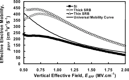
The effective electron mobility was measured on 1 µm (LG) by 10 µm (W) nMOSFETs
using the split CV technique [13]. The results of the measurement are shown in Fig. 1 where 100% mobility enhancement is observed in the strained Si nMOSFETs compared with the Si control device. The drain conductances (gDS) of 100 nm gate length MOSFETs are measured
using an impedance analyzer with a 10 MHz signal at the drain while biasing the gate. The measurement set-up can be used to extract the thermal resistance (RTH) of the MOSFET by
comparing the high frequency and DC gDS. Applying a high frequency drain-source signal
suppresses the effect of self heating, hence the intrinsic performance of the MOSFET can be measured. Details of the experimental set up are in the literature [5, 14-16]. The measured gDS
is integrated with respect to the drain voltage (VDS) so as to extract the output characteristics.
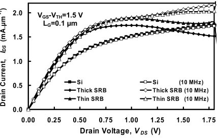
The resulting output characteristics of the 100 nm gate length nMOSFETs are shown in Fig. 2, where the drain currents (IDS) are shown as functions of VDS at 10 MHz and DC. It can be seen
in Fig. 2 that the strained Si nMOSFETs exhibit the negative gDS characteristic at high VDS due
to self heating at DC. This negative gDS characteristic is more severe in the strained Si
nMOSFET on the thick SiGe SRB. Fig. 2 also shows that the negative gDS characteristic
disappears at 10 MHz and the IDS enhancement compared with the Si control is restored. A
semi-empirical MOSFET model is used to calculate the temperature rise in the MOSFET channel by comparing the gDS at 10 MHz and DC [5, 14-16]. The RTH is then calculated by
dividing the temperature rise by the DC power, which is calculated as IDS.VDS. The RTH
extracted on the strained Si nMOSFET on the thick and thin SiGe SRB was calculated as 30.5
square-root of the buried oxide thickness. This model was subsequently applied to strained Si MOSFETs on SiGe SRBs in the work of Jenkin et al [18] and Agaiby et al [5]. Hence, by reducing the SRB thickness from 4 µm to 425 nm, the RTH is expected to reduce by 67%
whereas experimental measurements here show a reduction by 50%. This variation between the calculated and measured RTH percentage improvement in the thin SRB is due to the fact
that RTH is determined not only by the SRB thickness but also by other parameters like
phonon scattering from the Si/SiGe heterointerface, defects from strain relaxation in the virtual substrate as well as thermal boundary conditions around the channel (oxide interface, source/drain metal contacts, length of the Si3N4 sidewall spacer). In the work of Jenkin et al
[18], the RTH extracted for a 100 nm gate length strained Si nMOSFET on a 1.5 µm
Si0.85Ge0.15 SRB with a 15 nm strained Si channel layer was 13.4 K.mW-1. In the work of
Olsen et al [11], a RTH of 18.9 K.mW-1 and 4.5 K.mW-1was extracted from 0.4 µm gate length
strained Si nMOSFETs fabricated on 2 µm and 200 nm Si0.8Ge0.2 SRBs respectively with strained Si channel layers of 15 nm. The RTH values calculated here are comparable to what
has been published in literature for strained Si MOSFETs on SiGe SRBs [11, 18].
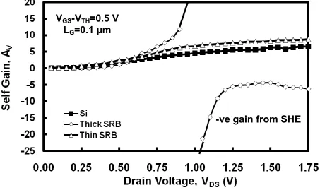
The self gain (AV) of the MOSFETs were calculated and shown as functions of VDS in
Fig. 3. The discontinuity in the AV characteristic of the strained Si nMOSFET on the thick
SiGe SRB in Fig. 3 is due to the change in polarity of the gDS, as it crosses to zero mark, due
to self heating. That this discontinuity in the AV vs. VDS characteristics does not occur in the
strained Si nMOSFET on the thin SiGe SRB is indicative of the fact that self heating is
reduced with buffer scaling. The equation of the MOSFET self gain taking self heating into account can be expressed as [12, 19]
DSN TH DSN
mN V
I R g
g A
θ
+
where gmN is the transconductance, gDSN is the drain conductance, IDSN is the drain current and
θ is the temperature sensitivity of the mobility. The discontinuity in the AV characteristic of
Fig. 3 occurs when the denominator in (1) is equal to zero.
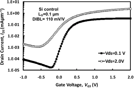
It can be seen from the DC output characteristics in Fig. 2 that drain induced barrier lowering (DIBL) is highest in the Si control device where a positive gDS is observable at high
VDS i.e. IDS does not fully saturate. DIBL can be calculated by measuring the change in the
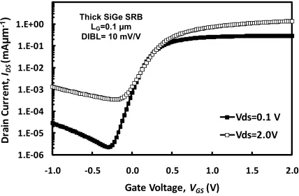
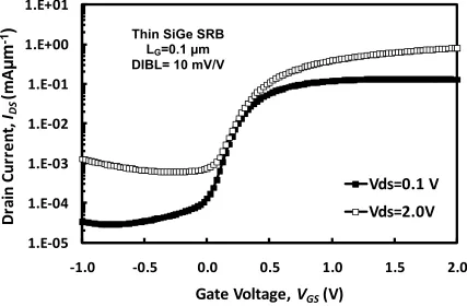
threshold voltage, VTH as VDS is increased. The gate transfer characteristics (IDS vs. VGS) for
the 100 nm gate length Si control, strained Si nMOSFET on the thick and thin SiGe SRB are
shown in Fig. 4(a), Fig. 4(b) and Fig. 4(c) respectively. The VGS spacing between the low VDS
and high VDS gate transfer characteristics in Fig. 4 is indicative of the extent of DIBL. DIBL is
calculated to be 110 mV/V for the 100 nm Si control nMOSFET whereas it is approximately 10 mV/V for the strained Si nMOSFETs on the thin and thick SiGe SRB. Self heating reduces the effect of DIBL in the strained Si devices since its impact on gDS is opposite to that of
DIBL.
III. TCAD MODEL
Electrothermal modeling of MOSFETs is traditionally done by solving the electron-hole drift-diffusion equations coupled with the heat flow equation. In the J.E
approach, the heat generated from current flow is calculated by taking the dot product of the
electric field, E, and current density, J (J.E) [7]. The total heat generated in the MOSFET is the sum of the heat generated from Joule heating and that from non-radiative electron-hole
become important. If the electrical carriers transit from the source to the drain before undergoing enough inelastic collisions to dissipate heat into the lattice, i.e. if there is insufficient time to thermalize, the J.E approach becomes less accurate since it assumes that
the carriers are in thermal equilibrium with the lattice. Non-local effects occur because carriers thermalize at distances several mean free paths away from the electric field peak, hence, in nanometer scale length devices, the peak of the electric field does not coincide with
the temperature peak. Furthermore, the Fourier heat diffusion law cannot accurately model heat flow at time scales on the order of magnitude of the phonon relaxation time [20]. Due to the limitations of the drift-diffusion approach for nanometer scale MOSFETs, heat conduction
is most accurately simulated by solving the Boltzmann transport equation for phonons [21]. These advanced simulation techniques are required for modeling nanoscale hot-electron
effects, temperature sensitive breakdown effects, impact ionization in nanoscale devices, device hot-spots and carrier velocity overshoot. Since the purpose of this study is limited to understanding the impact of self heating and –gDS on the circuit performance of 100 nm gate
length strained Si MOSFETs, the commercial device simulation software from Synopsys, MEDICI, is sufficient. The “lattice temperature advanced application” module in MEDICI was invoked to simulate self heating. To account for non-local effects, the hydrodynamic
carrier transport model is used to decouple the lattice temperature from the carrier temperature. The hydrodynamic model involves solving the energy balance equations coupled with the Poisson equation and the electron/hole continuity equations.
The strained Si MOSFETs are simulated in MEDICI by incorporating the values of the extracted and measured experimental parameters into the model. An average low field
extracted value is incorporated into the MEDICI model as a contact resistance in the electrode statement. An effective channel length of 85 nm, also extracted from the “shift and ratio” method, was incorporated into the MEDICI model by extending the source/drain regions into
the channel. The effective substrate doping is calculated from capacitance-voltage measurements [23] and incorporated into the MEDICI model. Table 1 shows lists the parameters measured or calculated and used in the MEDICI model. The thickness of the
strained silicon channel layer is defined as 10 nm in the mesh and the substrate terminal is defined as the thermal heat sink and set to 300 K. A lumped RTH element is defined and
connected to the 300 K heat sink as the thermal boundary condition. Setting appropriate and
realistic thermal boundary conditions for the source, drain and gate terminals are important because it affects the temperatures calculated. Setting no thermal boundary conditions
assumes adiabatic conditions in the MOSFET and hence represents the worst-case scenario of self heating since no heat flows out of the device. However the lumped RTH element
connected to the substrate will approximate the combined thermal boundary conditions for all
the terminals. The RTH is used as the variable for matching the measured data with the
simulated data. It is expected to be higher for the strained Si nMOSFET on the thick SiGe SRB because higher RTH values have been extracted experimentally.
IV. RESULTS AND DISCUSSION
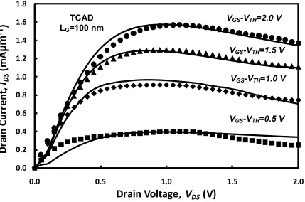
Fig. 5(a) shows the output characteristics simulated in MEDICI together with the
measured output characteristics where it can be seen that there is a good match for
VGS-VTH=0.5 V, 1 V, 1.5 V and 2 V. A lumped RTH of 1.4 x 10⁵ Kµm/W and 1 x 10⁵ Kµm/W
nMOSFET on the thick and thin SiGe SRB by 50% and 40% respectively. The RTH
determined by the simulations are smaller than those measured experimentally because the simulations assume no heat dissipation through the source, gate and drain terminals. Hence,
for the simulator to match the measured output characteristics, a substrate with a lower RTH is
required. Fig. 5(b) shows the measured and simulated output characteristics for the strained Si nMOSFETs and the Si control device at VGS-VTH=1.5 V where good matching can be
observed.
The MOSFET models were used in the “circuit analysis advanced application” module in MEDICI where the terminals were connected in an inverter configuration. Since
the mechanism of heat generation is similar for holes and electrons and the low thermal conductivity SiGe buffer is common to both devices, self heating also occurs in strained Si
pMOSFETs on SiGe SRBs [24, 25]. The pMOSFETs in the simulated inverter were not calibrated by measured data hence, the same self heating parameters defined for the nMOSFETs were used. Assuming the same RTH for the nMOSFET and pMOSFET is
reasonable since both devices will typically be fabricated on the same wafer. It was reported in the work of Rim et al [26] that hole mobility in tensile strained Si is slightly degraded compared with the Si control for low strain magnitudes and that high strain magnitudes are
required for hole mobility enhancement. The impact of low hole mobility on the output characteristics of the CMOS inverter will be to cause asymmetry in the switching characteristics by reducing the switching voltage. For symmetrical inverter operation, the gate
width of the pMOSFET used in the inverter simulations was set to 2.5 times that of the nMOSFET to compensate for lower carrier mobility. The voltage transfer characteristic
voltage gain equation can be expressed as
(
TH N DSN TH P DSP)
DSP DSN mP mN V I R I R g g g g A
θ
θ
+ − + + −= (2)
where gmP is the transconductance of the pMOSFET, gDSP is the output (drain)
conductance of the pMOSFET,
θ
N is the temperature sensitivity of the electron mobility,P
θ
is the temperature sensitivity of the hole mobility and IDSP is the pMOSFET draincurrent. The terms in the parenthesis in (2) account for self heating hence, setting RTH to zero
reduces (2) to the recognizable equation for the voltage gain of the CMOS inverting amplifier. The negative sign in (2) indicates that the amplifier inverts the input signal i.e. introduces a phase shift of 180˚ [16]. If the self heating terms in the parenthesis become larger than the
sum of the drain conductances, then the negative sign becomes positive thereby causing anomalous operation. It was reported in the work of Fox et al [19] that self heating causes
non-linear phase shifts and anomalous behavior in CMOS analog amplifiers.
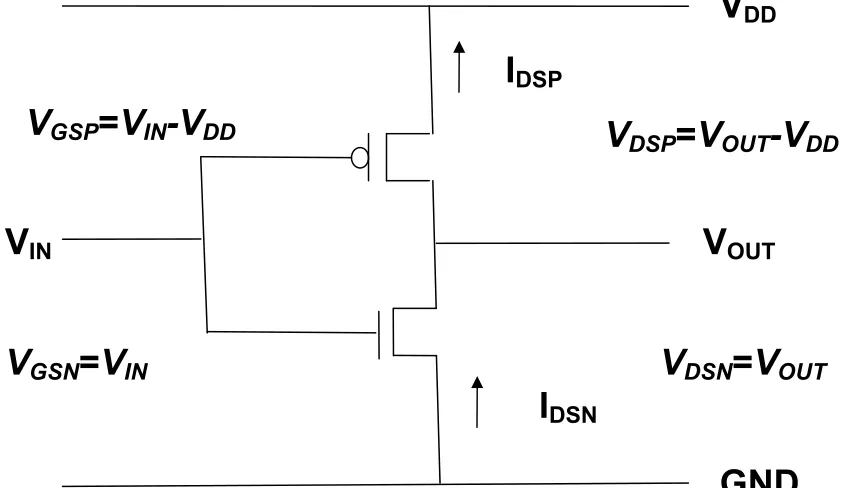
The VTC of the CMOS inverters were simulated for the Si control and strained Si devices with a power supply (VDD) of 2 V. The schematic of the inverter is shown in Fig. 6(a)
with the terminal voltages and currents labeled. In Fig. 6(a), VGSN is the gate-source voltage of
the nMOSFET, VGSP is the gate-source voltage of the pMOSFET, VDSN is the drain source
voltage for the nMOSFET, VDSP is the drain source voltage for the pMOSFET, VTHN is the
threshold voltage for the nMOSFET, VTHP is the threshold voltage of the pMOSFET and IDSP
is the drain source voltage of the pMOSFET. Fig. 6(b) shows the full VTC of the simulated CMOS inverters for the Si control and the strained Si nMOSFET on the thin SiGe SRB and
switching voltage, VS, is defined as the point on the VTC where the input voltage, VIN is equal
to the output voltage VOUT and is labeled in Fig. 6(b) as the intersection point between the
VTC and a 45° line from the graph origin. For a perfectly symmetrical inverter with identical
nMOS and pMOS characteristics, the inverter switches at VS=VDD/2. In the case of an inverter
with a relatively poorer pMOS performance (compared to nMOS) due to lower hole mobility in tensile strained Si (compared to electron mobility), the VS will be less than VDD/2 .i.e. the
VTC is shifted leftwards. It can be observed in Fig. 6(b) that the switching characteristic of the inverter with the thin SiGe SRB MOSFET is the most ideal because it has the highest switching slope. The voltage gain of the inverter is calculated by differentiating VOUT with
respect to VIN and is shown as a function of VIN in Fig. 7. The voltage gain of the inverter
simulated with the thin SiGe SRB MOSFET parameters is 300% higher than that of the Si
control. As in Fig. 6(b), the results of the thick SiGe SRB in Fig. 7 are inconclusive due to the inability of the simulator to converge. The impact of self heating on the output characteristics of the MOSFET is to reduce the gDS, whereas other short channel effects like drain induced
barrier lowering (DIBL) increase gDS. DIBL causes a positive gDS slope in IDS-VDS saturation
characteristics whereas self heating causes a negative gDS slope. Hence, balancing the
opposing effects of DIBL and self heating is key for optimal analog operation. For maximum
gain amplification, the gDS should be as little as possible especially for short channel devices
where high DIBL degrades the voltage gain [27]. The switching slope and voltage gain of CMOS inverters reduces as subthreshold conduction from DIBL increases. The interplay
between DIBL and self heating is responsible for the different voltage transfer characteristics shown in Fig. 6(b).
Fig. 8 shows how the VTCs are derived from the output characteristics of the respective devices. VOUT is the intersection point between the nMOSFET and pMOSFET
there can be only 1 solution for VOUT for any VIN. When VIN is zero, the nMOSFET is off
(VGSN=0 V and VDSN=VDD) and the pMOSFET is in the linear mode (VGSP=-VDD and VDSP=0
V). Since the pMOSFET is conducting, VOUT is equal to VDD and this is labeled in Fig. 8(a),
8(b) and 8(c) for the Si control, strained Si on thick SiGe SRB and strained Si on thin SiGe SRB respectively. As VIN increases towards VS, the nMOSFET goes into saturation (VGSN -
VTHN < VDSN) while the pMOSFET remains in the linear mode (VGSP - VTHP > VDSP). This part
of the VTC is labeled as VOUT1 in Fig. 8(a), 8(b) and 8(c). The VIN at which the nMOSFET
goes into saturation is a function of VTHN, which is strongly dependent on DIBL for short
channel devices. As shown in Fig. 4, DIBL is higher in the Si control nMOSFET due to the
absence of self heating hence the Si control inverter VTC shows “early switching” as labeled in Fig. 6(b). Because DIBL is low in the strained Si nMOSFETs, there is no early switching in
the VTC shown in Fig. 6. In this case, self heating is an advantage for the strained Si nMOSFETs on the thin SiGe SRB. The inverter switches state (VIN=VS) when both MOSFETs
go into saturation, which is labeled as VOUT2 in Fig. 8(a), 8(b) and 8(c). In the case of the
inverter VTC of the strained Si on thick SiGe SRB, (Fig. 8(b)), there is more than one intersection point between IDSN and IDSP, hence there is more than one solution for VOUT.
These multiple intersection points are due to the -gDS characteristics in Fig. 8(b) and are the
reasons why the simulator is unable to converge to a solution for VOUT in the thick SiGe SRB
VTC as shown in Fig. 6(b). This anomalous behavior due to self heating has previously been reported in analog silicon-on-insulator (SOI) circuits where non linear behavior was observed
in the output characteristics of inverters and CMOS amplifiers [19]. The output characteristics of the strained Si nMOSFET on the thin SiGe SRB (Fig. 8(c)) do not show multiple
intersection points and hence the simulator can converge to a solution for VOUT since there is
only one intersection point between IDSN and IDSP. As VIN is increased beyond VS, the
saturation (VGSP - VTHP < VDSP). This is labeled as VOUT3 in the respective characteristics of Fig.
8. Finally, VOUT reduces to zero as VIN reaches VDD.
The inverter VTC of the strained Si nMOSFET on the thin SiGe SRB exhibits the
highest voltage gain and best switching characteristics because DIBL is cancelled out by self heating. DIBL degrades the VTC of the Si control whereas self heating degrades the VTC of the thick SRB. Since both self heating and DIBL reduce as the gate length is increased, this
mutual cancellation becomes less critical for longer channel MOSFETs. It is hard to predict which effect will dominate at a specific gate length since DIBL depends on halo implants, channel implants, oxide thickness, junction depth, effective channel length, dopant
out-diffusion etc. On the other hand, self-heating depends on the Ge composition, layer thicknesses, physical dimensions, thermal boundaries, material quality etc. Although DIBL
and self heating are individually detrimental to the output characteristics of short channel MOSFETs, careful design of strained Si MOSFETs on SiGe SRBs can yield optimum analog performance if the effects are mutually cancelled out.
V. CONCLUSIONS
TCAD models have been calibrated by measured data, used to simulate the voltage transfer
characteristics of CMOS inverters and calculate the voltage gain of push-pull inverting amplifiers. Measured data and simulation results show that the thermal resistance is reduced by approximately 50% when the thickness of the SiGe SRB is reduced from 4 µm to 425 nm.
The voltage gain of the inverter simulated for the strained Si nMOSFET on the thin SiGe SRB exhibits 300% enhancement compared with the Si control inverter. This significant
strained Si nMOSFET on the thick SiGe SRB cause multiple solutions for the inverter output voltage, hence the simulator is unable to converge. The case is due to multiple intersection points between the drain currents due to negative conductance. This anomalous behavior is in
agreement with what has previously been reported in literature for analog SOI circuits. In the case of the Si control CMOS inverter, the voltage gain is limited by DIBL, which manifests itself in the voltage transfer characteristics as early switching. Although self heating and DIBL
are individually deleterious to the analog performance of MOSFETs, balancing their effects for maximizing voltage gain can yield positive results. The thickness of the SiGe SRB can therefore be used to control DIBL and optimize the voltage gain.
ACKNOWLEDGEMENT
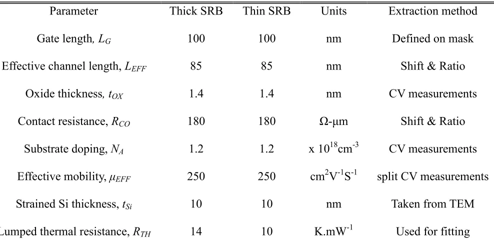
TABLE. 1. MOSFET PARAMETERS USED TO CALIBRATE MEDICI MODELS
Parameter Thick SRB Thin SRB Units Extraction method
Gate length, LG 100 100 nm Defined on mask
Effective channel length, LEFF 85 85 nm Shift & Ratio
Oxide thickness, tOX 1.4 1.4 nm CV measurements
Contact resistance, RCO 180 180 Ω-µm Shift & Ratio
Substrate doping, NA 1.2 1.2 x 1018cm-3 CV measurements
Effective mobility, µEFF 250 250 cm2V-1S-1 split CV measurements
Strained Si thickness, tSi 10 10 nm Taken from TEM
REFERENCES
[1] S. H. Olsen, A. G. O'Neill, S. Chattopadhyay, L. S. Driscoll, K. S. K. Kwa, D. Norris, A. Cullis, and D. J. Paul, "Study of single and dual channel designs of high performance strained Si/SiGe n-MOSFETs," IEEE Trans. Electron Devices, vol. 51, pp. 1245-1253, 2004.
[2] K. Rim, J. Hoyt, and J. Gibbons, "Analysis and fabrication deep submicron strained Si n-MOSFETs," IEEE Trans. Electron Devices, vol. 47, pp. 1406-1415, 2000.
[3] J. Dismukes, L. Ekstrom, E. Steigmeier, I. Kudman, and D. Beers, "Thermal and electrical properties of heavily doped Ge-Si alloys up to 1300 K," J. Appl. Phys., vol. 35, pp. 2899-2907, 1964.
[4] D. Cahill, F. Watanabe, A. Rockett, and C. Vining, "Thermal conductivity of epitaxial Layers of dilute SiGe alloys," Physical Rev. B, vol. 71, 2005.
[5] R. Agaiby, Y. Yang, S. H. Olsen, A. G. O'Neill, G. Eneman, P. Verheyen, R. Loo, and C. Claeys, "Quantifying Self-Heating Effects with Scaling in Globally Strained Si MOSFETs," Solid-State Electron., vol. 51, pp. 1473-1478, 2007.
[6] A. O'Neill, R. Agaiby, S. Olsen, Y. ang, P. Hellstrom, M. Ostling, M. Oehme, K. Lyutovich, E. Kasper, G. Eneman, P. Verheyen, R. Loo, C. Claeys, C. Fiegna, and E. Sangiorgi, "Reduced self heating by strained silicon substrate engineering," Appl. Surf. Sci, vol. 254, pp. 6182-6185, 2008.
[7] C. Fiegna, Y. Yang, E. Sangiorgi, and A. O'Neill, "Analysis of self heating effects in ultrathin-body SOI MOSFETs by device simulation," IEEE Trans. Electron Devices,
vol. 55, pp. 233-244, 2008.
[8] H. Herzog, T. Hackbarth, U. Seiler, U. Konig, M. Luysberg, B. Hollander, and S. Mantl, "Si/SiGe nMODFETs on thin SiGe virtual substrates prepared by means of He implantation," IEEE Electron Device Lett., vol. 23, pp. 485-487, 2002.
[9] T. Hackbarth, H. Herzog, F. Rinaldi, T. Soares, B. Hollander, S. Mantl, M. Luysberg, and P. Fichtner, "High frequency n-type MODFETs on ultra-thin virtual SiGe substrates," Solid-State Electron., vol. 47, pp. 1179-1182, 2003.
[10] K. Lyutovich, J. Werner, M. Oehme, E. Kasper, and T. Perova, "Characterisation of virtual substrates with ultra-thin Si0.6Ge0.4 strain relaxed buffers," Mat. Sci. Semicond.
Proc., vol. 8, pp. 149-153, 2005.
[11] S Olsen, E Cousin, J Varzgar, R Agaiby, J Seger, P Dobrosz, S Chattopadhyay, S Bull, A O'Neill, P Hellstrom, J Edholm, M Ostling, K Lyutovich, M Oehme, and E. Kasper., "Control of self heating in thin virtual substrate strained Si MOSFETs," IEEE Trans. Electron Devices, vol. 53, pp. 2296-2305, 2006.
[12] O. Alatise, K. Kwa, S. Olsen, and A. O'Neill, "Improved Analog Performance of Strained Si nMOSFETs on Thin Silicon-Germanium Strain Relaxed Buffers," In Proc. ESSDERC, pp. 99-102, 2008.
[13] D. Schroeder, "Semiconductor material and device characterization," Wiley, 1998. [14] B. Tenbroek, M. Lee, W. White, J. Bunyan, and M. Uren, "Impact of self heating and
thermal coupling on analog circuits in SOI CMOS," J. Solid-State Circuits., vol. 33, pp. 1037-1046, 1998.
[15] B Tenbroek, M Lee, W White, J Bunyan, and M. Uren, "Self heating effects in SOI MOSFETs and their measurement by small signal conductance technique," IEEE Trans. Electron Devices, vol. 43, pp. 2240-2248, 1996.
modeling of self heating in SOI MOSFETs," IEEE Trans. Electron Devices, vol. 41, pp. 69-65, 1994.
[18] K Jenkin and K. Rim, "Measurement of the effect of self heating in strained silicon MOSFETs," IEEE Electron Device Lett., vol. 23, pp. 360-362, 2002.
[19] M Fox and S. Brodsky, "Effects of self heating induced negative output conductance in SOI circuits," Proceedings in SOI Conference, pp. 152-153, 1993.
[20] E. Pop, "Self Heating in Scaled Thin Body Transistors," PhD Thesis, 2004.
[21] W. Liu and M. Asheghi, "Thermal modelling of self heating in strained silicon MOSFETs," Inter Society Conference on Thermal Phenomena, pp. 605-609, 2004. [22] Y. Taur, "MOSFET channel length: extraction and interpretation," IEEE Trans.
Electron Devices, vol. 47, pp. 160-169, 2000.
[23] S. Chattopadhyay, K. Kwa, S. Olsen, and A. O'Neill, "C-V characterization of strained Si/SiGe multiple heterojunction capacitors as a tool for heterojunction MOSFET channel design," Semicond. Sci. and Technol., vol. 18, 2003.
[24] M. Lei, Y. Hua, L. Chun, Y. Qi, Z. Jing, X. Jing, and T. Zhou, "Fabrication of strained Si channel pMOSFET on thin relaxed Si1-xGex virtual substrate," Proc. 7th
International Conference on Solid State and Integrated Circuits Technology, vol. 1, pp. 325-327, 2004.
[25] G Nicholas, T Grasby, E Parker, T Whall, and T. Stotnicki, "Evidence of reduced self heating in strained Si MOSFETs," IEEE Electron Device Lett., vol. 26, pp. 684-686, 2005.
[26] K Rim, J Chu, H Chen, K Jenkins, T Kanarsky, A Mocuta, H Zhou, R Roy, J Newbury, J Ott, K Petrarca, P Mooney, D Lacey, K Chan, D Boyd, M Ioeng, and H. Wong, "Characteristics and Device Design of Sub 100 nm Strained Si N and P MOSFETs," in Symp. VLSI Tech. Dig., pp. 98-100, 2002.
Fig. 1. The effective electron mobility as a function of the vertical effective field for the Si control and strained Si devices on the thin and thick SiGe SRBs. There is 100% mobility
enhancement in the strained Si devices compared with the Si control.
O Alatise
0
50
100
150
200
250
300
350
400
450
500
0.50
0.75
1.00
1.25
1.50
1.75
2.00
Vertical Effectiv e Field, E
EFF(MV.cm
-1
)
E
ff
e
c
ti
v
e
E
le
c
tr
o
n
M
o
b
il
it
y
,
µ
E F F(
c
m
2V
-1S
-1)
Si Thick SRB Thin SRB [image:20.595.82.517.82.354.2]Fig. 2. IDS vs. VDS characteristics with and without self heating effects on 0.1 µm gate length
MOSFETs at a gate overdrive VGS-VTH of 1.5 V.
O Alatise
0.0
0.5
1.0
1.5
2.0
0.00
0.25
0.50
0.75
1.00
1.25
1.50
1.75
Drain Voltage, V
DS(V)
D
ra
in
C
u
rr
e
n
t,
I
DS(
m
A
.µ
m
-1
)
Si Si (10 MHz ) Thick SRB Thick SRB (10 MHz ) Thin SRB Thin SRB (10 MHz )
V
GS-V
TH=1.5 V
Fig. 3. AV vs. VDS characteristics for the 100 nm gate length strained Si and bulk Si MOSFETs
measured at VGS-VTH=500 mV. Negative gDS due to self heating effects (SHE) causes negative
self-gain for the thick SiGe SRB devices at high VDS. This problem is eliminated by the thin
SRBs.
O Alatise
-ve gain from SHE
V
GS-V
TH=0.5 V
Fig. 4(a). IDS vs. VGS characteristics for the 100 nm gate length silicon control nMOSFET.
DIBL is calculated to be 110 mV/V. The separation between the 2 drain current curves shows
the impact of DIBL.
O Alatise
1.E-05
1.E-04
1.E-03
1.E-02
1.E-01
1.E+00
1.E+01
-1.0
-0.5
0.0
0.5
1.0
1.5
2.0
D
ra
in
C
u
rr
e
n
t,
I
DS(m
A
µ
m
-1
)
Gate Voltage,
V
GS(V)
Vds=0.1 V
Vds=2.0V
Si control
L
G=0.1 µm
[image:23.595.78.520.82.378.2]Fig. 4(b). IDS vs. VGS characteristics for the 100 nm gate length strained Si nMOSFET on the
thick SiGe SRB. DIBL is calculated to be 10 mV/V. The smaller separation between the drain current characteristics shows that the effect of DIBL is minimal.
O Alatise
1.E-06
1.E-05
1.E-04
1.E-03
1.E-02
1.E-01
1.E+00
-1.0
-0.5
0.0
0.5
1.0
1.5
2.0
D
ra
in
C
u
rr
e
n
t,
I
DS
(m
A
µ
m
-1
)
Gate Voltage,
V
GS(V)
Vds=0.1 V
Vds=2.0V
Thick SiGe SRB LG=0.1 µm
[image:24.595.77.505.84.364.2]Fig. 4(c). IDS vs. VGS characteristics for the 100 nm gate length strained Si nMOSFET on the
thin SiGe SRB. DIBL is calculated to be 10 mV/V. The smaller separation between the drain current characteristics shows that the effect of |DIBL is minimal.
O Alatise
1.E-05
1.E-04
1.E-03
1.E-02
1.E-01
1.E+00
1.E+01
-1.0
-0.5
0.0
0.5
1.0
1.5
2.0
D
ra
in
C
u
rr
e
n
t,
I
DS
(m
A
µ
m
-1
)
Gate Voltage,
V
GS(V)
Vds=0.1 V
Vds=2.0V
Thin SiGe SRB LG=0.1 µm
[image:25.595.77.504.83.363.2]Fig. 5(a). The simulated and measured output characteristics of the 100 nm gate length strained Si nMOSFET on the thick SiGe SRB. The results show good matching between the measured and simulated data.
O Alatise 0.0 0.2 0.4 0.6 0.8 1.0 1.2 1.4 1.6 1.8
0.0 0.5 1.0 1.5 2.0
D
ra
in
C
u
rr
e
n
t,
I
DS(m
A
µ
m
-1
)
Drain Voltage,
V
DS(V)
VGS-VTH=2.0 V
VGS-VTH=1.5 V
VGS-VTH=1.0 V
VGS-VTH=0.5 V
[image:26.595.80.509.78.362.2]Fig. 5(b). Simulated and measured output characteristics of the 100 nm gate length Si control
and strained Si nMOSFETs on the thick and thin SiGe SRBs. A lumped RTH of 1.4 x 10⁵
Kµm/W and 1.0 x 10⁵ Kµm/W was required to match the simulated output characteristics of the strained Si nMOSFET on the thick and thin SiGe SRB respectively.
O Alatise
0.0
0.2
0.4
0.6
0.8
1.0
1.2
1.4
1.6
1.8
0.00
0.25
0.50
0.75
1.00
1.25
1.50
1.75
D
ra
in
C
u
rr
e
n
t,
I
DS(m
A
.µ
m
-1
)
Drain Voltage,
V
DS(V)
Si
Thick SRB
Thin SRB
VGS-VTH=1.5 V
LG=100 nm
[image:27.595.79.533.82.369.2]Fig. 6(a). The schematic of the CMOS inverter with the currents and voltages labeled.
O Alatise
V
OUTV
DDV
DSP=V
OUT-V
DDV
DSN=V
OUTGND
V
INI
DSPI
DSNV
GSP=V
IN-V
DD [image:28.595.86.510.84.328.2]Fig. 6(b). The simulated voltage transfer characteristics of CMOS inverters for Si control and
strained Si nMOSFETs on thin and thick SiGe SRBs. Early switching due to DIBL is evident in the VTC of the Si control inverter. The simulator is unable to converge for the VTC of the strained Si nMOSFET on the thick SiGe SRB due to non-linear operation from self heating.
O Alatise
0.0
0.4
0.8
1.2
1.6
2.0
0.0
0.5
1.0
1.5
2.0
O
u
tp
u
t
v
o
lt
a
g
e
,
V
OU
T
(V
)
Input voltage,
V
IN(V)
Si
Thin SRB Thick VS
Early switching in Si control due to DIBL
Switching voltage, VS
[image:29.595.81.533.83.364.2]Fig. 7. The voltage gain of the push-pull inverting amplifier as a function of the input voltage for the Si control and strained Si on thin SiGe SRB inverters. There is 300% enhancement in
the voltage gain of the strained Si inverter compared with the Si control due to better switching characteristics.
O Alatise
-16
-14
-12
-10
-8
-6
-4
-2
0
0.0
0.5
1.0
1.5
2.0
In
v
e
rt
e
r
G
a
in
,
A
VInput voltage, V
IN(V)
Si
Thin SRB
Fig. 8(a). The simulated IDS vs. VDS characteristics of the inverter nMOSFET and pMOSFET
using models calibrated with the Si control nMOSFET parameters. The points of intersection
between IDSN and IDSP for VIN1, VIN2 and VIN3 are used to determine VOUT1, VOUT2 and VOUT3
respectively.
O Alatise
0.0
0.5
1.0
1.5
2.0
2.5
3.0
0.00
0.25
0.50
0.75
1.00
1.25
1.50
1.75
2.00
D
ra
in
C
u
rr
e
n
t,
I
DS(m
A
µ
m
-1
)
Output Voltage,
V
OUT(V)
VIN1 VIN2 VIN3 VIN1
VIN2
VIN3 VOUT1
VOUT2
VOUT3
VDD VOFF
[image:31.595.73.524.79.330.2]Fig. 8(b). The simulated IDS vs. VDS characteristics of the inverter nMOSFETs and pMOSFETs
using models calibrated with the strained Si nMOSFET on the thick SiGe SRB. Due to the negative gDS from self heating, there is more than one intersection point between IDSN and IDSP
for VIN2, hence the simulation fails to converge for a solution for VOUT2.
O Alatise
0.0
0.2
0.4
0.6
0.8
1.0
1.2
1.4
1.6
1.8
0.00
0.25
0.50
0.75
1.00
1.25
1.50
1.75
2.00
D
ra
in
C
u
rr
e
n
t,
I
DS(m
A
µ
m
-1
)
Output Voltage,
V
OUT(V)
VIN1 VIN2 VIN3 VIN1
VIN2
VIN3 VOUT1
VOUT2
VOUT3
VDD VOFF
[image:32.595.74.528.80.330.2]Fig. 8(c). The simulated IDS vs. VDS characteristics of the inverter nMOSFETs and pMOSFETs
using models calibrated with the strained Si nMOSFET on the thin SiGe SRB. The self heating is not enough to cause multiple intersection points for VIN2, hence, there is a solution
for VOUT2. The mutual cancellation between self heating and DIBL enables high voltage gain
and good switching characteristics.
O Alatise
0.0
0.5
1.0
1.5
2.0
2.5
0.00
0.25
0.50
0.75
1.00
1.25
1.50
1.75
2.00
D
ra
in
C
u
rr
e
n
t,
I
DS(m
A
µ
m
-1
)
Output Voltage,
V
OUT(V)
VIN1 VIN2 VIN3 VIN1
VIN2
VIN3 VOUT1
VOUT2
VOUT3
VDD VOFF
[image:33.595.77.536.80.331.2]Fig. 1. The effective electron mobility as a function of the vertical effective field for the Si control and strained Si devices on the thin and thick SiGe SRBs. There is 100% mobility enhancement in the strained Si devices compared with the Si control.
Fig. 2. IDS vs. VDS characteristics with and without self heating effects on 0.1 µm gate length
MOSFETs at a gate overdrive VGS-VTH of 1.5 V.
Fig. 3. AV vs. VDS characteristics for the 100 nm gate length strained Si and bulk Si MOSFETs
measured at VGS-VTH=500 mV. Negative gDS due to self heating effects (SHE) causes negative
self-gain for the thick SiGe SRB devices at high VDS. This problem is eliminated by the thin
SRBs.
Fig. 4(a). IDS vs. VGS characteristics for the 100 nm gate length silicon control nMOSFET.
DIBL is calculated to be 110 mV/V. The separation between the 2 drain current curves shows
the impact of DIBL.
Fig. 4(b). IDS vs. VGS characteristics for the 100 nm gate length strained Si nMOSFET on the
thick SiGe SRB. DIBL is calculated to be 10 mV/V. The smaller separation between the drain current characteristics shows that the effect of DIBL is minimal.
Fig. 4(c). IDS vs. VGS characteristics for the 100 nm gate length strained Si nMOSFET on the
thin SiGe SRB. DIBL is calculated to be 10 mV/V. The smaller separation between the drain
current characteristics shows that the effect of DIBL is minimal.
strained Si nMOSFET on the thick SiGe SRB. The results show good matching between the measured and simulated data.
Fig. 5(b). Simulated and measured output characteristics of the 100 nm gate length Si control and strained Si nMOSFETs on the thick and thin SiGe SRBs. A lumped RTH of 1.4 x 10⁵
Kµm/W and 1.0 x 10⁵ Kµm/W was required to match the simulated output characteristics of
the strained Si nMOSFET on the thick and thin SiGe SRB respectively.
Fig. 6(a). The schematic of the CMOS inverter with the currents and voltages labeled.
Fig. 6(b). The simulated voltage transfer characteristics of CMOS inverters for Si control and
strained Si nMOSFETs on thin and thick SiGe SRBs. Early switching due to DIBL is evident in the VTC of the Si control inverter. The simulator is unable to converge for the VTC of the strained Si nMOSFET on the thick SiGe SRB due to non-linear operation from self heating.
Fig. 7. The voltage gain of the push-pull inverting amplifier as a function of the input voltage for the Si control and strained Si on thin SiGe SRB inverters. There is 300% enhancement in
the voltage gain of the strained Si inverter compared with the Si control due to better switching characteristics.
Fig. 8(a). The simulated IDS vs. VDS characteristics of the inverter nMOSFET and pMOSFET
using models calibrated with the Si control nMOSFET parameters. The points of intersection
between IDSN and IDSP for VIN1, VIN2 and VIN3 are used to determine VOUT1, VOUT2 and VOUT3
Fig. 8(b). The simulated IDS vs. VDS characteristics of the inverter nMOSFETs and pMOSFETs
using models calibrated with the strained Si nMOSFET on the thick SiGe SRB. Due to the
negative gDS from self heating, there is more than one intersection point between IDSN and IDSP
for VIN2, hence the simulation fails to converge for a solution for VOUT2.
Fig. 8(c). The simulated IDS vs. VDS characteristics of the inverter nMOSFETs and pMOSFETs
using models calibrated with the strained Si nMOSFET on the thin SiGe SRB. The self heating is not enough to cause multiple intersection points for VIN2, hence, there is a solution
for VOUT2. The mutual cancellation between self heating and DIBL enables high voltage gain