Abstract—This paper investigates nature-inspired metaheuristics for optimized sizing of a CMOS comparator with PMOS input driver. The aim is to minimize MOS transistor area using two nature-inspired metaheuristics, differential evolution and harmony search. Simulation results demonstrate that design specifications are closely met and required functionalities are accommodated in short computational time while area optimization criterion is satisfied.
Index Terms—constrained optimization, analog integrated circuits, automated design, transistor sizing, metaheuristics
I. INTRODUCTION
OGETHER with the increase in integrated circuit (IC) complexity, the design and optimization complexity of analog integrated circuits has increased drastically [1]. Even, the design of an analog circuit consists of a few transistors may be more challenging than designing a fairly complex digital circuit. This is mainly due to the lack of predefined libraries of analog standard cells contrary to digital systems [2]. Moreover, characterization of complex tradeoffs between nonlinear objectives while satisfying required specifications and constraints makes analog circuit design a long and tedious process [3,4].
Transistor sizing is a constrained optimization problem and resides between topology selection and actual circuit layout of analog design problem. Considering CMOS IC sizing process, several relations should be hold between width/length ratio of MOS transistors to ensure that constraints and specifications are satisfied. Besides, design parameters such as MOS dimension ratios should be adjusted in order to meet optimization objectives. These complicated and time consuming processes should be automated with high accuracy in a reasonable operation time which requires efficient optimization methods.
Heuristics are proposed to solve high dimensional problems with many criteria. They can be adapted to suit specific problem requirements [5, 6, 7]. Heuristics can be divided into two classes: on the one hand, there are algorithms which are specific to a given problem and, on the other hand, there are generic algorithms, i.e., metaheuristics
Dr. Revna Acar Vural is with Yildiz Technical University, Department of Electronics and Communication Engineering, Davutpasa Campus, 34220, Turkey. (corresponding author; phone: +902123835919; e-mail: racar@ yildiz.edu.tr).
Ufuk Bozkurt and Prof. Dr. Tulay Yildirim is with Yildiz Technical University, Department of Electronics and Communication Engineering, Davutpasa Campus, 34220, Turkey.
[8]. Metaheuristics designate a computational method that optimizes a problem by iteratively trying to improve a candidate solution with regard to a given measure of quality. Notable examples of metaheuristics include genetic algorithm (GA), simulated annealing (SA), particle swarm optimization (PSO), genetic programming (GP), ant colony optimization (ACO), differential evolution (DE) and harmony search (HS). A detailed investigation of metaheuristics based analog circuit sizing is reviewed in [9,10].
Much research work has been devoted to metaheuristics based transistor sizing of basic analog building blocks such as operational amplifiers [2-4,11-18], differential amplifiers [3,19] and operational transconductance amplifiers [20-24]. This is mainly due to the fact that they are at the heart of many interface circuit, in particular digital-to-analog converters (DAC), analog-to-digital converters (ADC) and filters. An efficient design of optimal basic analog blocks is thus a cornerstone of a design environment for many applications.
Among those researches, PSO is used for CMOS transistor area minimization of a two-stage operational amplifier [3,4] and maximizing both gain and unity gain bandwidth of a complementary folded cascade operational amplifier [11]. In [12], SA is combined with gm/ID characteristics and ACM MOSFET model for both area and power minimization of a two- stage Miller operational amplifier. A heuristic method is proposed for area optimization of a telescopic cascade amplifier and two-stage operational amplifier [2,13]. ACO is utilized for minimization of both area and power consumption of a two-stage operational amplifier [14]. Competitive co-evolutionary DE method is proposed to minimize power consumption in operational amplifiers [15]. DE method is also used for operational transconductance amplifier (OTA) sizing considering power minimization and gain maximization in [20]. In [21], together with DE, HS is applied to automated sizing of folded cascode OTA. A very detailed operational amplifier synthesis method based on GP is given in [16]. GP is also proposed for minimizing power consumption in different OTA structures [22,23]. GA is probably the most widely used metaheuristics in automation of analog IC transistor sizing. Noise minimization [17] and gain maximization [17,18] objectives of a two-stage operational amplifier are accomplished with GA method. Power consumption of a differential amplifier is minimized using GA based transistor sizing in [19]. In [20], results obtained with DE are compared to that of canonical nondominated sorting GA (NSGA-II). NSGA-II based sizing
Metaheuristics Based CMOS Two-Stage
Comparator Optimization
Revna Acar Vural, Ufuk Bozkurt and Tulay Yildirim
methodology proves its efficiency in optimization of Miller OTA by minimizing power consumption and maximizing gain.
Different from abovementioned studies, this work focuses on optimal sizing of a CMOS comparator with metaheuristics based synthesis methodology. Here, MOS transistor area is aimed to be minimized in short computation time while satisfying design specifications and design constraints. Section II describes metaheuristics used in this study. Design procedure of CMOS comparator is given in section III. Following, simulation results of proposed methods are provided in section IV. Finally, section V concludes with a discussion of metaheuristics based design results and suggests possible extensions.
II. METAHEURISTICS
Metaheuristics are iterative in nature and may move to not necessarily improving solutions which avoids being stuck at local minima [5,6,25]. DE and HS are two nature inspired metaheuristics used for CMOS comparator sizing. Details of those are provided in the following subsections.
A. Differential Evolution
DE is a real coded population-based optimization method based on parallel direct search method and diverges from GA by adding the weighted difference between two chromosomes to the third in order to generate new ones [26].
DE uses a population P having NP individuals that evolves over G generations to reach the optimal solution. Each individual X is a vector that features a dimension size of D. Each vector in population matrix is assigned follows.
Xj=Xjmin+Șj(Xjmax-Xjmin), j= 1,…,D (1) where Xjmax, Xjmin are the upper, lower bounds, respectively and Șj is a uniformly distributed random number within [0,1] of the jth feature. The optimization process in DE is carried out using three basic operators; mutation, crossover and selection. The mutation operator generates mutant vectors (X’) as in (2).
Xi’(G) = Xa(G)+F(Xb(G) – Xc(G)), abcI (2) where Xa, Xb and Xc are randomly selected vectors among population matrix including NP different vectors. F is the scaling constant used to improve algorithm convergence. The crossover operation is employed to create trial vectors (X’’) by mixing the individuals of the mutant vectors (X’) with the target vector (X) according to (3).
(3)
where q is a randomly chosen index within [1,NP], guaranteeing that trail vector employs at least one individual from the mutant vector. CR is the crossover constant within [0,1] that controls the population diversity. Finally selection operator compares the fitness values of trial vectors and
target vectors. If trial vectors yield better fitness values then they replace the target vectors with which they were compared, otherwise predetermined population member is retained. The above procedure restarts until the chromosomes have been successfully updated to improve their fitness values to a specified value [26, 27].
B. Harmony Search
HS is a metaheuristics method based on the improvisation process of jazz musicians [28]. HS searches an optimal combination of inputs by usage of harmony memory, pitch adjusting and randomization just as musicians seek a fantastic harmony by playing any known tune from their memory, playing a similar tune or composing new and random notes.
Initial population structure of HS is very similar to that of DE as explained in the previous subsection. Here, the total number of individuals is equal to harmony memory size (HMS) and individuals are stored in harmony memory (HM). Following, a new solution is improvised according to harmony memory considering rate (HMCR). A stored value is chosen from HM with probability of HCMR (0HCMR
1) and 1-HCMR is the probability of generating it randomly. If the solution is picked from HM, it is mutated according to the pitch adjust rate (0PAR 1). After HM is updated the fitness values are evaluated. If the improvised solution yields a better fitness than that of the worst member in HM, it replaces the worst one. Otherwise the improvised one is eliminated. The above procedure is repeated until a preset termination criterion (maximum iterations or a target fitness value) is met [21, 28].
III. DESIGN PROCEDURE FOR CMOSCOMPARATOR
[image:2.595.313.555.542.768.2]A comparator is a device that compares two voltages or currents and switches its output to indicate which is larger. They are commonly used in analog-to-digital converters (ADCs), data transmission, switching power regulators, and many other applications [29,30].
Fig. 1. Comparator with PMOS input driver [29]
°¯ ° ®
≤ =
=
otherwise X
q j or CR if
X X
G j i
j G j i G j i
,
) ( ) (
,
) (
,
' ) ( '
, ) ( '' ,
(
)
(
)
2) ( 6 6 6
2
/
SAT DS P DSV
K
I
L
W
=
¸¸ ¹ · ¨¨ © § + − = 7 6 6 2 ds ds m V g g g AThe problem considered here is the optimal selection of CMOS transistor dimensions for comparator with PMOS input driver (Fig.1), which is only a part of a complete analog circuit CAD tool. It can be characterized by a number of specifications as given below.
• Common Mode Rejection Ratio (CMRR) • Slew Rate (SR)
• Power Dissipation (Pdiss)
• Small Signal Characteristics (Av, f-3dB) • Input Common Mode Range (ICMR) • Power Supply Rejection Ratio (PSRR)
These performance metrics as well as design objective(s) have to be formulated in terms of the design variables. Here, design objective which can be defined as CF is the minimization of the occupied MOS transistor area as in (4).
CF
¦
(
)
= = T i i i xL W 1 ) ( )
( (4)
Providing limits for design constraints of small-signal differential voltage gain (Av), cutoff frequency (f-3dB), maximum and minimum input common mode voltages (VIC(max), VIC(min)), slew rate (SR), power dissipation (Pdiss) and design variables of external resistor (Rb) and MOS device sizes, general design procedure can be summarized below [30].
•Determine the current drive requirement of (W/L)7 to
satisfy the SR specification.
( )
SR C dt dV CID L ¸¸= L
¹ · ¨¨ © § = 7 (5)
•Determine the size of (W/L)6 and (W/L)7 to satisfy the
output-voltage swing requirement.
(6)
(
)
(
)
2) ( 7 7 7
2
/
SAT DS P DSV
K
I
L
W
=
(7)•Calculate the gain of the second stage.
(8)
•Calculate the gain of the first stage to satisfy the overall gain.
10000
2
1
≥
=
V VV
A
A
A
(9)
•Determine the first stage biasing current using the minimum allowable size of 1
•Consider (W/L)4 and (W/L)6; using the minimum size
for (W/L)4, determine the current ISD4 that mirror with
(W/L)6.
(
)
(
)
66 4 4 / / DS DS I L W L W I = (10) 4
5
2
DSSD
I
I
=
(11)
•Consider (W/L)5 and (W/L)7; using the minimum size
for (W/L)5, determine the current IDS5 that mirror with
(W/L)7.
(
)
(
)
77 5 5 / / SD SD I L W L W I = (12) 3 5
4 SD
/
2
DSDS
I
I
I
=
=
(13)
2
/
5 1
2 SD SD
SD
I
I
I
=
=
(14)
•Select the larger of the two ISD4 and adjust the size of
(W/L)4 if necessary.
•Determine the size of (W/L)1 to satisfy the gain
requirement. The minimum size of (W/L)5 can be adjusted to
satisfy the positive ICMR.
(
)
[
(
)
]
1 2 1 1 1 2 / SD P P N SD V I K I A LW = λ +λ
(15)
(
)
11 1 (max) 1 ) ( 5 / 2 T P SD G DD SAT SD V L W K I V V
V = − − −
(16)
(
)
(
)
2) ( 5 5 5 2 / SAT DS P SD V K I L W = (17)
•Select the larger of the two, (W/L)5 and adjust the size
of (W/L)7 for proper mirroring with (W/L)5. The size of
(W/L)3 or (W/L)4 can be adjusted to meet the negative input
CMR.
(
)
(
)
55 7
7 /
/ W L
I I L W = (18)
(
)
(
)
21 3 (min) 1 3 3 2 / T T SS G P DS V V V V K I L W + − − = (19)
•Select the larger of the two (W/L)3.
•Determine the size of (W/L)8 to provide as the main
current mirror for the comparator.
(
)
(
)
28 8 8
2
/
TP SG P SDV
V
K
I
L
W
−
=
(20)•The external resistor Rb connected between VG8 and
ground must be chosen to provide the required current for (W/L)8. 8 8
0
DS G bI
V
R
=
−
IV. SIMULATION RESULTS
In this work, by establishing design parameters and specifications to metaheuristics, the optimal sizing is aimed to be automated by DE and HS. The aim is to minimize total MOS transistor area while satisfying design specifications and design parameter constraints.
First of all, a certain range is determined for both design specifications and design parameters by human designer. The inputs to the DE and HS based design schemes are those abovementioned ranges for each design parameter and specification as well as preferential technology parameters and supply voltage values. Metaheuristics should minimize given CF and obtain design criteria and design parameter values for the given range which provides minimum CF value.
Considering CMOS comparator, DE and HS are utilized for design specifications of VDD=2.5V, VSS=-2.5V,
AV>10000, -1.65V<ICMR<1.65V, Pdiss<1000µW and
SR>10V/us considering an output capacitance of 10pF. Simulations are carried out using TSMC 0.35µm technology parameters. In order to minimize the channel modulation effect, all MOSFET length values are chosen as 2µm. Target value of CF is aimed to be smaller than 500µm2.
Design scheme is implemented with the relationships that describe design specifications to solve for DC currents and dimension ratios of all MOS transistors. Algorithms are constructed using MATLAB R2008a. Here, cost function evaluation and design parameter/specification range control are processed in separate procedural loops. Thereby, updates will not be carried out unless specified ranges are satisfied and better CF values are obtained. Instead of using penalty functions we choose that kind of a “fail” strategy. Flowchart of metaheuristics based design scheme is provided in Fig. 2.
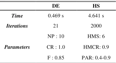
DE based comparator design is concluded in 0.469 s which is approximately ten times faster compared to HS based design method. Computational performance and algorithm parameters of each method are given in Table I.
TABLEI
COMPARISON OF COMPUTATIONAL PERFORMANCE
DE HS
Time 0.469 s 4.641 s
Iterations 21 2000
Parameters
NP : 10 HMS: 6
CR : 1.0 HMCR: 0.9
F : 0.85 PAR: 0.4-0.9
Design variables obtained with DE and HS methods are tabulated in Table II. Total MOS transistor area and resistor values obtained with both methods are approximately same. Area and resistor value obtained with HS is slightly smaller than the ones obtained with DE. However, DE based design achieves a better ICMR than HS based method.
In order to validate metaheuristics based design is satisfying desired specifications comparator with PMOS input driver is redesigned using the resulting design
[image:4.595.73.266.553.658.2]parameters (Table II) in SPICE simulator. SPICE simulations (Figs 3-8) demonstrate that DE and HS based designs not only satisfy all specifications but also minimize total MOS area as given in Table III. Simulations are run on Intel Core 2 Duo CPU, T7300 @ 2.00GHz.
Fig. 2. Flowchart of metaheuristics based design scheme
TABLEII
DESIGN VARIABLES OBTAINED WITH METAHEURISTICS
Comparator
Design Parameters DE HS
W1/L1, W2/L2 (µm/µm) 20.057/2 24.230/2
W3/L3, W4/L4 (µm/µm) 2/2 2/2
W5/L5 (µm/µm) 6.899/2 6.386/2
W6/L6 (µm/µm) 58.396/2 58.182/2
W7/L7 (µm/µm) 100.72/2 92.894/2
W8/L8 (µm/µm) 20.071/2 18.579/2
Rb(kȍ) 68.383 67.827
TABLEIII
COMPARISON OF DE AND HS BY MEANS OF DESIGN CRITERIA
Comparator
Design Criteria Specifications DE HS
Slew Rate (V/µs)
≥
10 160 160 Power Dissipation(µW)
≤
1000 511 508Unity Gain
Bandwidth (MHz)
≥
10 16.055 17.255 Gain (dB) > 80 82.424 82.932Vicmin (V)
≥
-1.65 -1.6042 -1.6146Vicmax (V)
≤
1.65 1.6458 1.5938CMRR (dB) > 85 87.4715 87.8223
Propagation Delay
(us) < 2 1.165 1.111
Total Area
Fig. 3. Gain of DE based comparator design
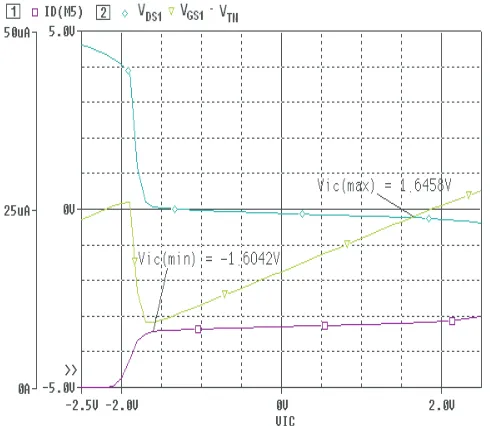
[image:5.595.46.291.258.471.2]Fig. 4. ICMR of DE based comparator design
Fig. 5. Propagation delay of DE based comparator design
[image:5.595.310.546.259.472.2]Fig. 6. Gain of HS based comparator design
Fig. 7. ICMR of HS based comparator design
[image:5.595.51.292.505.718.2] [image:5.595.303.550.506.716.2]V. CONCLUSION
The problem considered here is the optimal selection of MOS transistor sizes of a comparator structure considering area minimization as the design objective. In addition, particular specifications are aimed to be met by adjusting design variables such as device sizes and resistor. In order to automate those design tasks, metaheuristics are proposed. Simulations demonstrate that DE based design requires very few iterations and is ten times faster than HS. Resulting design variables are utilized for redesign in SPICE simulator in order to validate the exact values of design specifications obtained with metaheuristics. Simulation results proved that DE and HS based design meets all design specifications and also minimizes total MOS area. As further work, performance of other heuristic methods could be investigated by utilizing EKV modeling in analog sizing issues.
REFERENCES
[1] G.Gielen, R.A. Rutenbar, “Computer-aided design of analog and mixed signal integrated circuits”, Proc. of IEEE, vol. 88, 2000, pp. 1825-1852.
[2] J. Puhan, A. Burmen, T. Tuma, “Analogue integrated circuit sizing with several optimization runs using heuristics for setting initial points”, Canadian J. of Electrical and Computer Eng., vol.28, 2003, pp.105-111.
[3] R. A. Vural, T. Yildirim, “Analog circuit sizing via swarm intelligence”, AEU Int. J. of Electronics and Comm, vol.66, 2012, pp. 732-740.
[4] R. A. Vural, T. Yildirim, “Swarm intelligence based sizing methodology for CMOS operational amplifier”, Proc. of 12th IEEE Symp. on Computational Intelligence and Informatics, 2011, pp.525-528.
[5] E.G. Talbi, “A Taxonomy of Hybrid Metaheuristics”, Journal of Heuristics, 2002, pp. 541-564.
[6] M. Basseur, E.G. Talbi, A. Nebro, E. Alba, “Metaheuristics for Multiobjective Combinatorial Optimization Problems: Review and Recent Issues”, National Institute of Research in Informatics and Control (INRIA), report no.5978, September 2006.
[7] M. Fakhfakh, M. Loulou and N. Masmoudi, “A novel heuristic for multiobjective optimization of analog circuit performance”, Analog Integrated Circuits and Signal Processing, vol. 61, 2009, pp. 47-64. [8] M. Fakhfakh et. al, “Analog Circuit Design Optimization Through
the Particle Swarm Optimization Technique”, Analog Integrated Circuits Signal Processing, vol. 63, 2010, pp.71-82.
[9] E. Roca, M. Fakhfakh, R. Castro-López, F. V. Fernández, ”Applications of evolutionary computation techniques to analog, mixed-signal and RF circuit design - an overview”, Proc. of 16th IEEE Int. Conf. on Electronics, Circuits and Systems, 2009, pp. 251-254.
[10] E. Tlelo-Cuautle et. al,“Applications of evolutionary algorithms in the design automation of analog integrated circuits”, Journal of Applied Sciences, vol.10, 2010, pp. 1859-1872.
[11] V. Ceperic, Z. Butkovic and A. Baric, “Design and optimization of self-biased complementary folded cascode”, Proc. of IEEE Mediterranean Electrotechnical Conference (MELECON), 2006, pp. 145-148.
[12] A. Girardi, and S. Bampi, “Power constrained design optimization of analog circuits based on physical gm/Id characteristics”, Journal of Integrated Circuits and Systems, vol. 2, 2007, pp. 22-28.
[13] P.K. Meduri, “A novel methodology for design automation of CMOS operational amplifiers”, Proc. of Int. Symp. on Electronic System Design (ISED), 2010, pp.181-186.
[14] B. Bachir , A. Ali and M. Abdellah, “Multiobjective optimization of an operational amplifier by the ant colony optimisation algorithm”,
Electrical and Electronic Engineering, vol.2, 2012, pp. 230-235. [15] B. Liu et. al., “Analog circuit optimization system based on hybrid
evolutionary algorithms”, Integration VLSI J., vol.42, 2009, pp.137-148.
[16] M. Hershenson, S.P. Boyd and T.H. Lee, “Optimal design of a CMOS op-amp via geometric programming”, IEEE Trans. CAD Integrated Circuits Systems, vol. 20, 2001, pp. 1–21.
[17] J. Yu and Z. Mao, "Automated design method for parameters optimization of CMOS analog circuits based on adaptive genetic algorithm", Proc. of 7th Int. Conf. on ASIC, 2007, pp: 1217-1220.
[18] P.P. Kumar, K. Duraiswamy and A.J. Anand, “An optimized device sizing of analog circuits using genetic algorithm”, European Journal of Scientific Research, vol.69, 2012, pp. 441-448.
[19] L. C. Severo and A. Girardi, “Automatic synthesis of analog integrated circuits using genetic algorithms and electrical simulations”, Proc. of 24th South Symp. on Microelectronics, 2009, pp.1-5.
[20] A.M. Anile et. al. “Comparison among evolutionary algorithms and classical optimization methods for circuit design problems”, Proc. of IEEE Cong. on Evolutionary Computation, 2005, pp. 765–772. [21] S. Kudikala, S. L. Sabat and S. K. Udgata, “Performance study of
harmony search algorithm for analog circuit sizing”, Proc. of Int. Symp. on Electronic System Design, 2011, pp.12-17.
[22] J. Oliveros, D. Cabrera, E. Roa and W. V. Noije, “An improved and automated design tool for the optimization of CMOS OTAs using geometric programming”, Proc. of 21st Annual Symp. on Integrated Circuits and System Design, 2008, pp.146-151.
[23] W. Gao and R. Hornsey, “A power optimization method for CMOS op-amps using sub-space based geometric programming”, Proc. of IEEE Design Automation and Test in Europe, 2010, pp. 508-513. [24] C. Goh, Y. Li, “Multi-objective synthesis of CMOS operational
Amplifiers using a hybrid genetic algorithm”, Proc.of 4th Asia-Pacific Conf. on Simulated Evolution and Learning, 2002, pp. 214– 218.
[25] M. Gendreau and J.Y. Potvin, Handbook of Metaheuristics, International Series in Operations Research and Management Science, Springer, 2010.
[26] R. Storn, K. Price, “Differential Evolution: A simple and Efficient Adaptive Scheme for Global Optimization over Continuous Spaces”, Journal of Global Optimization, vol. 11,1997, pp. 341-359.
[27] J. Olensek, A. Burmen, J. Puhan and T. Tuma, Automated Analog Electronic Circuits Sizing, Differential Evolution:Fundamentals and Applications in Electrical Engineering, Chap.13, John Wiley & Sons, 2009, pp. 353-367.
[28] Z.W.Geem, J. H. Kim ,G. V. Loganathan, “A new heuristic optimization algorithm: harmony search”, Simulation, vol. 76, 2001, pp. 60-68.
[29] S. Kale and R. S. Gamad, “Design of a CMOS comparator for low power and high speed”, Internationl Journal of Electronic Engineering Research, vol. 2, 2010, pp. 29-34.
![Fig. 1. Comparator with PMOS input driver [29]](https://thumb-us.123doks.com/thumbv2/123dok_us/470974.545286/2.595.313.555.542.768/fig-comparator-pmos-input-driver.webp)