AN-17
DDR SDRAM Memory Termination
AN-17
USING THE LX1672 AND LX1673
FOR DDR SDRAM MEMORY
TERMINATION
LX1672 Protected by US Patents: 6,285,571 & 6,292,378
Copyright © 2002
Microsemi
Revision 1.2b, 3/8/2006 Integrated Products
11861 Western Avenue, Garden Grove, CA. 92841, 714-898-8121, Fax:: 714-893-2570
AN-17
DDR SDRAM Memory Termination
Page 2
T
ABLE OFC
ONTENTS 1.0 INTRODUCTION... 3 2.0 SDR vs DDR SDRAM ... 4 3.0 TERMINATION METHODS ... 5 4.0 SSTL_2 TERMINATION ... 55.0 SSTL_2 DRIVERS and RECEIVERS ... 7
6.0 SSTL_2 VOLTAGES... 7
7.0 VTT and VREF... 8
8.0 LX1672 CONTROLLER ... 9
AN-17
DDR SDRAM Memory Termination
1.0
I
NTRODUCTIONThe demand for higher memory speeds has resulted in evolution of the established PC100 / PC133 SDRAM to the newer Double Data Rate (DDR) SDRAM which clocks data on both positive and negative transitions of the clock, two data transfers per clock cycle result in a data rate of 266 MHz while the command and address lines only transition on the positive clock edges for a 133 MHz rate, speed grades for DDR allow for both 200 MHz and 266 MHz data transfer rates.
At higher data rates it is necessary to terminate the bus accurately to manage ringing and reflections. Stub Series Terminated Logic (SSTL) has been developed to allow data rates of 266MHz as required for DDR SDRAMs. JEDEC has released a specification (EIA/JESD8-9A) that defines I/O levels and conditions for operation with SSTL_2 , for 2.5 volt levels vs. the 3.3 volts used in PC133.
A new terminating voltage (VTT) is required as a supply for the terminating resistors and the line driver / receiver supply ( VDDQ)
is a second new supply voltage required by DDR SDRAM.
The LX167X family of synchronous buck controllers can supply the power required for the termination voltage. The three members of this family LX1671,72,73 have either three, two, or one PWM controllers and one linear regulator controller. Power requirements in addition to VTT can be met with the additional controllers. The LX1672 can supply both VDDQ and VTT using
Copyright © 2002
Microsemi
Revision 1.2b, 3/8/2006 Integrated Products
11861 Western Avenue, Garden Grove, CA. 92841, 714-898-8121, Fax:: 714-893-2570
AN-17
DDR SDRAM Memory Termination
Page 4
2.0
SDR
VSDDR
SDRAM
DDR memory systems are configured in the same way as the PC133 SDRAM with many similarities in the DIMM packaging and communication protocols, however significant differences exist. The internal addressing , command control interface, and refresh requirements are identical.
Some key differences are the reduction in VDD and VDDQ voltages to 2.5 volts and the requirement for a terminating voltage (VTT), there is also a reference voltage
(VREF) that is used on one side of the differential line
receiver. The new voltages VREF and VTT must meet the
JEDEC standard to insure proper data transmission. VTT
has a unique feature in that it must source and sink current.
The DDR clock is a differential signal and allows data transfer on both positive and negative transitions, all other lines are single ended, DDR also uses a new bi-directional data strobe. SDR memory employed a fixed voltage level for signal interface and while DDR data is still single ended the addition of VREF on the negative side of the line
receiver allows symmetrical data transfer with superior noise immunity, lower voltage swings on the signal lines, and less jitter.
Table 1 shows some of the key differences between SDR and DDR memory systems with emphasis on DC voltages since memory commands are not the focus of this document.
PARAMETER SDR DDR COMMENTS
VDD and VDDQ 3.3 V 2.5V Lower power requirements for DDR VREF N/A 1/2 VDDQ Used on line receiver negative input
VTT N/A = VREF Supply for terminating resistors
Data Rate 1X Clock 2X Clock DDR has a Differential Clock
Signal Interface LVTTL SSTL_2 DDR --- JEDEC standard EIA/JESD8-9A
Table 1 – SDR vs DDR Key Differences (Partial List)
AN-17
DDR SDRAM Memory Termination
3.0
TERMINATION
METHODS
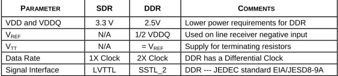
Several methods shown in Figure 1 can be used to terminate a transmission line into its characteristic impedance to minimize ringing and reflections. From the power dissipation point of view there are significant differences that must be taken into account when a large number of lines are being terminated.
(Fig 1a) Shows a simple resistor to ground with no power dissipation when data is low, dissipation is VDD2 / RT+RS) for a high signal. Although this works well for single ended lines power consumption is data dependant. The open circuit voltage is zero which will not work with the line receiver used for SSTL.
The second method (Fig 1b) uses two resistors on each line. The Thevenin equivalent is a terminating resistor of RTΩ and an open circuit voltage of VDD/2. For RS=RT power dissipation for both high and low signals is (3 VDD)2 / 8RT. If the data line is floating there is a constant power dissipation of VDD2/4RT.
A third method (Fig 1c) uses a single resistor connected to a terminating voltage VDD/2. For either a high or low signal the dissipation is (VDD/2)2 / (RT+RS). There is no power dissipated when the line is floating. This offers a three to one power dissipation advantage over the Thevenin termination with only one termination resistor and also has an open circuit voltage of VDD/2.
RS RT VDD VSS VDD VSS RS 2RT VDD VSS VDD VSS 2RT VDD RS VDD VSS VDD VSS RT VDD/2
a - Grounded Termination resistor
b - Thevinin Termination
c - Termination Resistor Connected To VDD / 2
Figure 1 – Three Bus Termination Methods
4.0
SSTL_2
TERMINATION
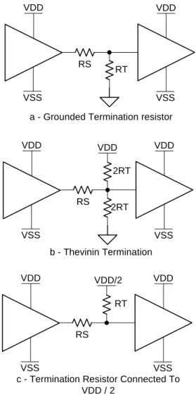
Some key differences between SSTL_2 and Figure 1c are the addition of a different supply voltage for the line driver (VDDQ), a termination voltage (VTT), and the
reference voltage (VREF) on the negative input of the line
receiver .
The SSTL_2 specification requires a minimum signal level, at the input of the line receiver, of 380 mV above and below VREF with the line driver Vout at its maximum
high and low voltages. Two classes of termination (Class I and II), Figures 2 and 3, are specified and are intended for different line drivers
Power dissipation in RT and RS is determined by the current output of the line driver which will determine the magnitude of the signal swing. With worst case conditions for a Class II line driver the maximum current in RT could be 31.8 mA ( see section 7.0).
There are several other termination methods allowed by the SSTL_2 specification that are not in wide spread use and are not shown here.
Copyright © 2002
Microsemi
Revision 1.2b, 3/8/2006 Integrated Products
11861 Western Avenue, Garden Grove, CA. 92841, 714-898-8121, Fax:: 714-893-2570
AN-17
DDR SDRAM Memory Termination
Page 6 RS 25Ω RT 50Ω VDDQ VSS VDD VSS VREF = VREF + -VTT
Figure 2 – SSTL_2 Class I Termination
RS 25Ω RT 50Ω VDDQ VSS VDD VSS VREF = VREF RT 50Ω = VREF +
-V
TTV
TTFigure 3 – SSTL _2 Class II Termination
SSTL_2 Class I is used with line drivers having a minimum of 7.6 mA sink or source capability and Class II is used with line drivers having a minimum of 15.2 mA sink and source capability. A variation of Class II is to
use a single 25Ω termination resistor at the line receiver. In either case the effective RT is 25Ω resulting in the same current demand on the VTT supply.
AN-17
DDR SDRAM Memory Termination
5.0
SSTL_2
D
RIVERS ANDR
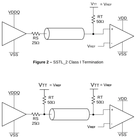
ECEIVERSFigure 4 shows the basic configuration for the driver and receiver used with SSTL_2. The driver in Fig 4a is not much different from line drivers used in PC133 but has greater drive capability. The receiver in Fig 4b has a differential input and a reference voltage on one side. The data is single ended but must be centered on the VREF
voltage for best noise margins, this gives very good performance since the two transistors are matched and the threshold voltage can be tightly controlled by VREF.
Figure 4a
OUT VDDQ VSSQ VSS DATA INPUT VOUT VDDQ = 2.5V VREF Figure 4BFigure 4 – SSTL_2 Line Driver and Receiver
6.0
SSTL_2
V
OLTAGESJEDEC standard JESD8-9A contains values for the key voltages which are summarized in Table 2
SYMBOL PARAMETER MIN NOMINAL MAX UNITS
VDD Device Supply Voltage VDDQ
VDDQ Output Supply Voltage 2.3 2.5 2.7 V VREF Input Reference Voltage 1.15 1.25 1.35 V
VTT Termination Voltage VREF -.04 VREF VREF +.04 V
Copyright © 2002
Microsemi
Revision 1.2b, 3/8/2006 Integrated Products
11861 Western Avenue, Garden Grove, CA. 92841, 714-898-8121, Fax:: 714-893-2570
Page 8
AN-17
DDR SDRAM Memory Termination
Some points to keep in mind when working with these values.
1 VDD is not specified but must be greater than or equal to VDDQ (3.3 V is allowed although the DDR SDRAM specification JESD79 calls for a migration to 2.5 V)
2 VREF is one half of VDDQ (plus or minus 8%) and
must track it at all times. (The JEDEC specification allows deviation from VDDQ/2 but most designers will stay with nominal values.)
3 VTT must be within 3.2% of VREF.
4 VTT must track any changes in VREF over all
operating conditions.
5 The peak to peak noise on the VREF line must not
exceed +/-2% of the VREF DC value. This only
allows 25mV of noise.
6 There is no specification for noise on the VTT
voltage.
7.0
VTT
ANDVREF
VREF is only used as an input to devices with very lowinput current so does not need a low source impedance except for the requirement to keep noise within the 25mV limit. VREF can be supplied by the output of an operational
amplifier with appropriate bypassing but this may cause stability problems with the amplifier. A simple and easy VREF source is to use a resistive divider from VDDQ and
bypass it at a number of locations with capacitors to the VDDQ and VSSQ rails. The balanced bypassing helps to insure that VREF is kept midway between VDDQ and
VSSQ even in the presence of transients.
10K Ω 10K Ω VDDQ VDDQ VDDQ VSSQ VSSQ VSSQ VREF .1 uF .1 uF .1 uF .1 uF
Figure 5 – VREF Divider and Bypassing
The receiver uses VREF as one side of the its input so any
noise or deviation in VREF voltage will result in timing
errors and jitter. A number of bypass capacitors (ceramic multilayer) located at each DIMM will keep the noise within specification. As always good layout techniques are essential.
Since VTT is used to supply current to the terminating
resistors it must have a low source impedance and be able to supply enough current for the number of lines to be terminated.
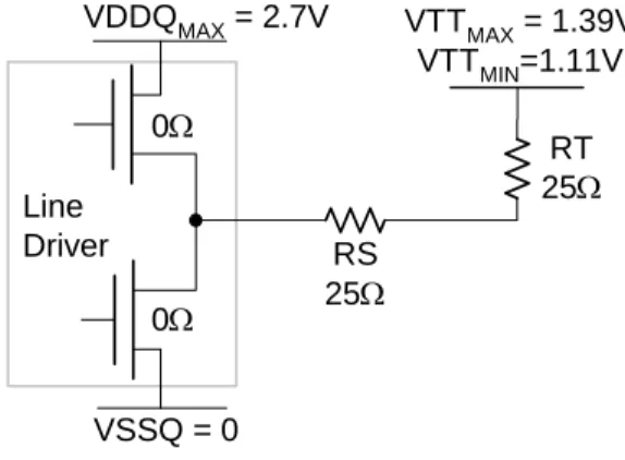
Using worst case conditions (VDDQ max = 2.7V, VTT min
= 1.11V, VTT max = 1.39 V and 0 Ω driver output
resistance) but nominal 25 Ω RS and RT.
A driver could source (Figure 10)
(VDDQ max-VTT min) / (RT+RS) = 31.8 mA of VTT
current when high, or sink
VTT max / (RT+ RS) = 27.8 mA when low.
The assumption of a 0 Ω driver is made because SSTL-2 specifies only the minimum output driver current.
RS 25Ω RT 25Ω VSSQ = 0 VDDQMAX = 2.7V VTTMAX = 1.39V VTTMIN=1.11V Line Driver 0Ω 0Ω
Figure10 – Worst Case RT current
Under nominal conditions (VDDQ=2.5 V and VTT = 1.25
V) the line driver can source or sink 25 mA per line with a 0 Ω output impedance line driver. A bus with equal distribution of high and low signals would place no demand on the VTT supply, however a bus that had all
high or all low signals could source or sink currents of several amperes, even with nominal values. VTT must be
supplied by a low output impedance source to remain within specification as the loads change.
AN-17
DDR SDRAM Memory Termination
8.0
LX1672
CONTROLLER
With a number of DIMMs operating from 2.5 volts and the need to generate VTT at a significant amount of current
two new voltages are now required on the motherboard. The LX1672 is a dual PWM that can supply both voltages and output current can be scaled to suit the specific board requirements. The LX1671 with three PWMs and the LX1673 with one PWM can be substituted if applicable. The PWM controllers are nearly identical on all devices. The VTT voltage must track VREF and be able to source and
sink current depending on the state of the data. A supply topology that meets this requirement is a synchronous buck regulator with an error amplifier input that can be connected to an external reference voltage. The LX1672 has one PWM with the error amplifier inputs pinned out. VREF can be connected directly to the positive error
amplifier input to insure that VTT will be at one half of
VDDQ and stay within tolerance over changes in the VDDQ voltage as required by the SSTL_2 specification. Due to the relatively high currents required for a large number of terminating resistors, 2A to 6 A, the VTT supply
should be as close as possible to the terminating resistors
and use wide etch in both the VTT and return paths, a
number of bypass capacitors (.1uf ceramic multilayer) should located at the terminating resistors.
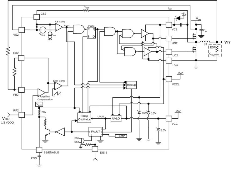
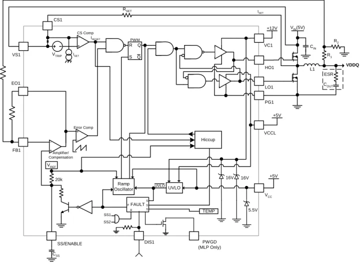
Figures 6 and 7 are block diagrams showing the LX1672 developing both VTT and VDDQ from a 3.3 volt input,
Figure 8 is a schematic of the same configuration showing the complete solution to develop both voltages. The LDO is not shown but could be connected if a third output is required.
When an external reference is used the connection between the error amplifier positive input and the Soft Start pin is lost and Soft Start will not function. It is recommended that the external reference voltage have an R-C time constant that will be long enough to allow the output capacitor to charge slowly.
For details on circuit operation, component selection , and other circuit configurations see the Microsemi LX1672 Data Sheet and LX1672 Product Design Guide or equivalent documents for the LX1671 and LX1673.
Copyright © 2002
Microsemi
Revision 1.2b, 3/8/2006 Integrated Products
11861 Western Avenue, Garden Grove, CA. 92841, 714-898-8121, Fax:: 714-893-2570
Page 10
AN-17
DDR SDRAM Memory Termination
CS Comp + -Amplifier/ Compensation + -Error Comp + -IRESET R S Q Q VTRIP 20k VREF Hiccup Ramp Oscillator UVLO L3 ESR COUT CIN VIN +5V VTT RSET VCC LO2 HO2 VC2 CS2 FB2 SS/ENABLE ISET PWM ISET +5V EO2 VS2 VCCL PG2 UVLO RF2 FAULT TEMP SS1 SS2 F R S S S +5V CSS DIS 2 16V 16V 5.5V VREF = 1/2 VDDQ
AN-17
DDR SDRAM Memory Termination
CS Comp + -Amplifier/ Compensation + -Error Comp + -IRESET R S Q Q VTRIP 20k VREF Ramp Oscillator UVLO L1 R1 ESR COUT R2 CIN +12V VIN(5V) +5V VDDQ RSET CSS VCC LO1 HO1 VC1 CS1 FB1 SS/ENABLE ISET PWM ISET +5V EO1 VS1 VCCL PG1 UVLO Hiccup FAULT TEMP SS1 SS2 F R S S S 5.5V DIS1 PWGD (MLP Only) 16V 16VCopyright © 2002
Microsemi
Revision 1.2b, 3/8/2006 Integrated Products
11861 Western Avenue, Garden Grove, CA. 92841, 714-898-8121, Fax:: 714-893-2570
Page 12
AN-17
DDR SDRAM Memory Termination
R5 Q1 L1 + Q2 C10 C4 +5V +3.3V + R4 R3 R2 R1 C5 Q3 Q4 + +3.3V L2 + R8 R6 R7 VTT 1.25V VDDQ 2.5V
HO2
LO2
PG2
LDGD
LDFB
LDDIS
DGND
AGND
DIS2
SS2
RF2
FB1
EO1
CS1
VS1
VCC
VCCL
PG1
LO1
HO1
VC1
VC2
FB2
SS1
EO2
DIS1
CS2
VS2
VREF =1/2 VDDQ CR2 C12 +5V CR1 C11 +5V C9 C6 C1 C7 + + C2 C8AN-17
DDR SDRAM Memory Termination
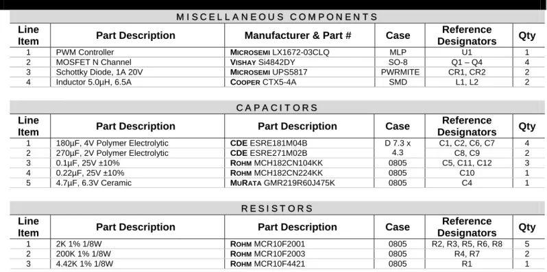
M I S C E L L A N E O U S C O M P O N E N T S
Line
Item Part Description Manufacturer & Part # Case
Reference Designators Qty
1 PWM Controller MICROSEMI LX1672-03CLQ MLP U1 1
2 MOSFET N Channel VISHAY Si4842DY SO-8 Q1 – Q4 4
3 Schottky Diode, 1A 20V MICROSEMI UPS5817 PWRMITE CR1, CR2 2
4 Inductor 5.0µH, 6.5A COOPER CTX5-4A SMD L1, L2 2
C A P A C I T O R S
Line
Item Part Description Part Description Case
Reference Designators Qty
1 180µF, 4V Polymer Electrolytic CDE ESRE181M04B C1, C2, C6, C7 4
2 270µF, 2V Polymer Electrolytic CDE ESRE271M02B
D 7.3 x 4.3 C8, C9 2 3 0.1µF, 25V ±10% ROHM MCH182CN104KK 0805 C5, C11, C12 3 4 0.22µF, 25V ±10% ROHM MCH182CN224KK 0805 C10 1 5 4.7µF, 6.3V Ceramic MURATA GMR219R60J475K 0805 C4 1 R E S I S T O R S Line
Item Part Description Part Description Case
Reference Designators Qty
1 2K 1% 1/8W ROHM MCR10F2001 0805 R2, R3, R5, R6, R8 5
2 200K 1% 1/8W ROHM MCR10F2003 0805 R4, R7 2
3 4.42K 1% 1/8W ROHM MCR10F4421 0805 R1 1
Copyright © 2002
Microsemi
Revision 1.2b, 3/8/2006 Integrated Products
11861 Western Avenue, Garden Grove, CA. 92841, 714-898-8121, Fax:: 714-893-2570
Page 14
AN-17
DDR SDRAM Memory Termination
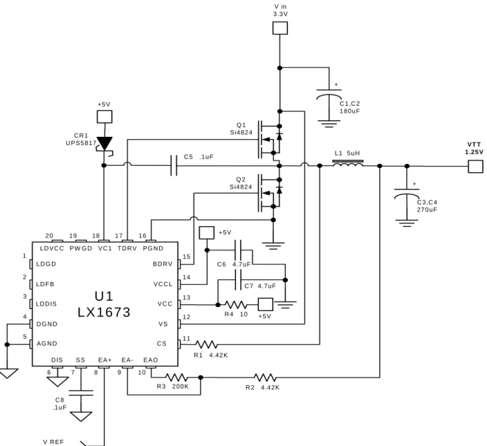
9.0 LX1673 CONTROLLER
The LX1673 single phase PWM controller may be used to generate two output voltages if the internal LDO controller is used. Figure 10 is a block diagram of the LX1673 showing its use as a single output VTT supply. Figure 11 is a schematic of
the LX1673 configured for a VTT supply with the LDO feature
not being used.
When an external reference is used the connection between the error amplifier positive input and the Soft Start pin is lost and Soft Start will not function. It is recommended that the external reference voltage have an R-C time constant that will be long enough to allow the output capacitor to charge slowly.
CS Comp + -Amplifier/ Compensation + -Error Comp + -IRESET R S Q Q VTRIP 20k VREF Hiccup Ramp Oscillator UVLO L1 ESR COUT CIN +5V VTT 1.25V RSET VCC BDRV TDRV VC1 CS EA-SS ISET PWM ISET +5V EAO VS VCCL PGND UVLO EA+ FAULT TEMP F R S S S +5V CSS 5.5V 16V 16V VREF =1/2 VDDQ SS1 DIS 3.3V
AN-17
DDR SDRAM Memory Termination
U 1
L X 1 6 7 3
L D G D L D F B L D D IS D G N D A G N D L D V C C P W G D V C 1 T D R V P G N D B D R V V C C L V C C V S C S E A O E A -E A + S S D IS + 5 V + 5 V + 5 V 1 2 3 4 5 6 7 8 9 1 0 1 1 1 2 1 3 1 4 1 5 1 6 1 7 1 8 1 9 2 0 C 8 .1 u F R 3 2 0 0 K R 2 4 .4 2 K R 1 4 .4 2 K C 6 4 .7 u F C 7 4 .7 u F C 5 .1 u F C R 1 U P S 5 8 1 7 Q 1 S i4 8 2 4 C 1 ,C 2 1 8 0 u F C 3 ,C 4 2 7 0 u F L 1 5 u H V R E F = 1 /2 V D D Q Q 2 S i4 8 2 4 V in 3 .3 V + + R 4 1 0 V T T 1 .2 5 VCopyright © 2002
Microsemi
Revision 1.2b, 3/8/2006 Integrated Products
11861 Western Avenue, Garden Grove, CA. 92841, 714-898-8121, Fax:: 714-893-2570
Page 16
AN-17
DDR SDRAM Memory Termination
M I S C E L L A N E O U S C O M P O N E N T S
Line
Item Part Description Manufacturer & Part # Case
Reference Designators Qty
1 PWM Controller MICROSEMI LX1672-03CLQ MLP U1 1
2 MOSFET N Channel VISHAY Si4842DY SO-8 Q1 – Q2 2
3 Schottky Diode, 1A 20V MICROSEMI UPS5817 PWRMITE CR1 1
4 Inductor 5.0µH, 6.5A COOPER CTX5-4A SMD L1 1
C A P A C I T O R S
Line
Item Part Description Part Description Case
Reference Designators Qty
1 180µF, 4V Polymer Electrolytic CDE ESRE181M04B C1, C2 2
2 270µF, 2V Polymer Electrolytic CDE ESRE271M02B
D 7.3 x 4.3 C3, C4 2 3 0.1µF, 25V ±10% ROHM MCH182CN104KK 0805 C5, C8 2 4 4.7µF, 6.3V Ceramic MURATA GMR219R60J475K 0805 C6, C7 2 R E S I S T O R S Line
Item Part Description Part Description Case
Reference Designators Qty
1 10 Ohm, 1% 1/8W ROHM MCR10F10R0 0805 R4 1
2 200K 1% 1/8W ROHM MCR10F2003 0805 R3 1
3 4.42K 1% 1/8W ROHM MCR10F4421 0805 R1, R2 2