Abstract—The Ion-Sensitive Field-Effect Transistor (ISFET) has traditionally been used to measure hydrogen ion concentration (pH) of a solution. Its performance depends mainly on its sensitivity to pH change of the electrolyte in contact with its gate. This sensitivity is usually calculated by examining the effect of pH value on the charge and potential distributions above gate insulator, which is translated into a shift in the threshold voltage. In this work, we propose a methodology to extract the sensitivity of ISFET by linking electrolyte charge and potential equations with a device simulation tool to calculate the ISFET’s drain current, thus, taking into account the underlying structure’s physical properties. Using the proposed methodology, the sensitivity of ISFET is compared for various pH values and gate-insulator thicknesses searching for the optimum conditions that give the highest sensitivity.
Index Terms—ISFET, pH-sensor, biosensors, device simulation.
I. INTRODUCTION
Ion-Sensitive Field-Effect Transistor (ISFET) has been used for detection of the ionic activity in an electrolyte solution attached to the gate oxide of a Metal-Oxide-Semiconductor (MOS) structure. One of the most useful parameters to be measured in biochemistry is the hydrogen concentration, or pH. ISFET is one of the leading pH sensors using semiconductor technologies [1]. It has recently attracted more interest because of many advantages compared to other pH sensing methods such as litmus papers and glass pH electrodes [2], [3]. It has a relatively high sensitivity, smaller size, and it can be used at high temperature. Moreover, it suits continuous monitoring, has potential for large-scale integration, and may be fabricated using conventional CMOS process. ISFETs have been adopted in various lab-on-chip and health-care applications [4]. It found use also in agriculture, environmental monitoring, and food industries [2].
Manuscript received September 25, 2014; revised January 10, 2015. Sponsor and financial support acknowledgment: This work was supported by the Deanship of Scientific Research, Umm Al-Qura University, Makkah, Saudi Arabia under Grant 43408011”.
Tarek M. Abdolkader and A. G. Alahdal are with the Electrical Engineering Department, Faculty of Engineering, Umm Al-Qura University, Saudi Arabia, on leave from Benha University, Benha, Egypt (e-mail: tmhasan@ uqu.edu.sa, [email protected]).
A. Shaker and W. Fikry are with the Engineering Physics Department, Ain Shams University, Egypt (email: [email protected], [email protected]).
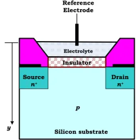
metal gate of the latter is replaced by an electrolyte solution to be tested, with a reference metal electrode immersed in this electrolyte. A change in the hydrogen ion concentration of the electrolyte (pH change) induces a change in the charge distribution on the surface of the gate insulator and this will in turn change the drain current ID in the MOSFET [5]. pH
measurement may be done by relating it to the change in drain current ID at a fixed reference electrode voltage (Vref).
In this case, the sensitivity is expressed as ID change per pH
unit change. Alternatively, pH may be measured by finding the required Vref shift to maintain fixed ID value. [2]. Here, it
becomes the change in Vref per pH unit change.
Source Drain
Reference Electrode
Electrolyte
Insulator
Silicon substrate y
n+ n+
p
Fig. 1. Schematic diagram of ISFET structure.
As the sensitivity of an ISFET is an important parameter determining its performance, many attempts for modeling it were reported [3], [6]-[8]. All these attempts use an approximate analytical expression to describe the electrostatics of the underlying MOSFET.
Although ISFETs have been fabricated in CMOS for a variety of physical geometries, it has not yet been reported how design dimensions impact sensor characteristics [6]. In this work, we propose a methodology for extracting the sensitivity of the ISFET using full numerical simulation of its underlying MOSFET, and thus, include the effect of MOSFET structure parameters more accurately. The proposed methodology is used to compare the ISFET sensitivity at the whole pH range, and for various current levels and reference voltage values. In addition, the effect of the gate-insulator thickness is also examined. This helps to optimize the ISFET performance by choosing the most suitable conditions of operation.
Section II reviews ISFET theory depicting its electrostatic equations. Section III presents the new proposed
ISFET pH-Sensor Sensitivity Extraction Using
Conventional MOSFET Simulation Tools
Tarek M. Abdolkader, Abdurrahman G. Alahdal, Ahmed Shaker, and Wael Fikry
Protonated Positively charged site Electrolyte
O O O O O O O H
H H
Deprotonated Negatively charged site Insulator
IHP OHP
+
+
+ +
+
Helmholtz Layer Diffuse Layer
+
Fig. 2. Binding sites and double electrical layer at electrolyte-insulator interface.
II. ISFET THEORY
ISFET operation is explained using site-binding theory [9]. The insulating surface of the ISFET’s gate contains hydroxyl groups (OH) that forms binding sites. They can be positively charged (by acquiring H+) or negatively charged (by losing H+) depending on the concentration of the hydrogen ions in the electrolyte. Accordingly, the insulating surface is charged with surface charge density that depends on the solution’s pH.
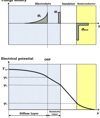
According to Gouy–Chapman–Stern theory [9], electrolyte ions (anions and cations) form three regions ( Fig. 2). The first extends from the Insulator-Electrolyte interface to the Inner Helmholtz Plane (IHP), which is the plane passing through the centers of the specifically adsorbed ions. Next, the region from IHP to the Outer Helmholtz Plane (OHP)that passes through the centers of the hydrated ions at their distance of closest approach to the solid. The third region consists of a diffuse charge region extending from the OHP into the electrolyte bulk, which is referred to as the Gouy-Chapman layer [7].
As shown in Fig. 3(a), the charge distribution along the
y-direction (the direction normal to the interface) can be divided into three parts: 1) the inversion/depletion charge in the semiconductor channel, σMOS, 2) the surface charge on the
Insulator-Electrolyte interface resulting from ion adsorbing,
σo, and 3) the continuous charge distribution through the
diffuse layer, σd. The corresponding potential distribution is
depicted in Fig. 3(b), in which, Vref, ψd, ψo, and ψs are the
electric potentials at the reference gate electrode, the edge of diffuse layer (OHP), the electrolyte-insulator interface, and the semiconductor-insulator interface, respectively.
Applying Gauss Law using a Gaussian surface which encompasses the whole structure, we can write [5], [8],
0
d o MOS
(1)Electrolyte Insulator
OHP
Semiconductor
σd
Helmholtz Layer Diffuse Layer
ψs
ψo
ψd
Vref
σo
σMOS
Charge density
y
y Electrical potential
Fig. 3. (a) Surface charge density and (b) potential distribution in an Electrolyte-Insulator-Semiconductor (EIS) system along y-direction (the
direction normal to the interface).
0
(
)
8
sinh
2
ref d
d o w
q V
kTc
kT
(3)where w is dielectric constant of water, c0 is the solution ion
concentration.
Second, the surface charge density of the binding sites on the insulator interface, σo, is given by [5], [8],
2
2
[
]
[
]
[
]
[
]
[
]
s
o sil
s s
s nit
s N
K K
qN
K
K K
qN
K
H
H
H
H
H
(4)
where Nsil and Nnit are the number of silanol sites and primary
amine sites per unit area, respectively; K+, K-, and KN+ are the
dissociation constants for positively charged silanol sites, negatively charged silanol sites, and positively charged amine sites, respectively; [H+]s is the concentration of
protons at the insulator surface.
The first term in the above equation, σd, can be related to ψd
and ψousing a Gaussian surface that encompasses the diffuse
layer charge and passing through the Helmholtz layer
(
)
d
C
h d o
(2)where Chis the capacitance of the Helmholtz layer.
In addition, solving Poisson equation in the diffuse layer results in an expression for σdin terms of ψdwhich is given as
It should be noted that [H+]s is related to the concentration
of protons inside the electrolyte bulk, [H+]b by [8]
(
)
[
]
[
] exp
ref os b
q V
kT
H
H
(5)where the pH of the solution is –log([H+]b).
The third type of charge density, σMOS, is related to ψo and
ψs through Gauss law
(
)
MOS
C
ins s o
(6)where Cins is the capacitance of the insulator.
Another equation that is needed to solve the system is the relation representing the effect of underlying MOSFET structure on the surface potential and charge density [8]
0
1/ 2
2
1 exp
1 exp
MOS o Si
s s
o s s
o
kTp
q
q
kT
kT
n
q
q
p
kT
kT
(7)
where Si is dielectric constant of silicon; no and po are the
equilibrium electron and hole concentrations within silicon. The seven equations (1)-(7) has seven unknowns: three charge densities, three surface potentials, and [H+]s, so, they
can be solved simultaneously to get all potentials. Once ψo is
known, the shift in the threshold voltage is determined by (Vref – ψo) [9], so, the new threshold voltage will be,
'
(
)
T T ref o
V
V
V
(8)where VT is the threshold voltage of the basic MOSFET
structure. Once VT'is known, the drain to source current can be found analytically using any of the standard MOSFET models [10]. For example, simple charge control model can be used to get the drain current [3],
' '
' 2 '
( / 2) ( )
( ) / 2 ( )
n ins D
G T D D D G T
G T D G T
W C
I
L
V V V V V V V
V V V V V
(9)
Two ways can be used to express ISFET sensitivity: the first is using S1 defined as the absolute value of change in ID
per unit change in pH with Vref fixed, so
1
(constant)
ref
D
V
I
S
pH
(10)The second is using S2 defined as the absolute value of
change in Vref per unit change in pH that is required to
maintain ID fixed
2
(constant)
D
ref
I
V
S
pH
(11)Once the drain current ID is calculated for a certain
reference voltage Vref at a certain pH, ID is found again for a
neighboring pH value, and S1 is found from (10). Similar
procedure can be used for S2.
III. PROPOSED SIMULATION METHOD
Calculation of ISFET sensitivity presented in the last section uses approximate modeling equations to describe MOSFET electrical properties. This is represented by equations (6)-(9) which are based on simplifying assumptions to reach closed-form analytical formulae. On the other hand, numerical device simulation of MOSFET represents device physics more accurately and takes into account process effects more deeply. So, in this work, we replace these modeling equations by linking ISFET charge and potential equations (1)-(5) to the numerical device simulation tool, Silvaco [11] in order to find a complete solution of the system. The methodology is shown in the flow chart in Fig. 4 and explained hereinafter.
pH = pH(initial)
Assume a value for ψo
Use MOSFET simulator to find
ψs, σMOS and ID
Solve equations (1) – (8) to find
Vref(cal)
|δ| < tol
δ = Vref(cal)–Vref ψo = ψo - δ
Output ID
pH = pH(final) pH = pH+δpH
End No
Yes
No
Yes
Fig. 4. Flow chart for the methodology proposed for the extraction of ISFET sensitivity.
certain reference electrode voltage Vref, a value of ψo is
assumed (roughly half of the reference electrode voltage,
Vref). Then, a device simulation using Silvaco tools is
performed for a conventional metal-gated MOSFET with its gate bias equals ψo. From the simulation results we can
calculate ψs, σMOS, and ID. Now, equations (1)-(5) can be
solved for the unknowns: σo, σd, ψd, Vref, and [H+]s and,
consequently, a new value of Vref is found which we call it
Vref(cal).The calculated Vref(cal) is compared to the real value of
the reference electrode voltage, Vref, and the difference is
subtracted from the firstly assumed ψo. Now, the new
updated value of ψo is used to perform a new simulation run.
The whole process is repeated until the difference between the calculated and real values of Vref is within a certain
tolerance. After reaching a consistent solution for both ψo and
Vref, the drain current output from simulation is stored for the
corresponding value of pH and Vref.
If, conversely, the drain current ID is predetermined and it
is required to find the corresponding reference voltage Vref
that produces this current at certain pH, simulation runs are repeated with ψo incremented until it produces the
predetermined current, then, equations (1)-(5) are solved only once to get Vref.
All calculations are repeated for different pH values. Once
ID and Vref are known for each value of pH, (10) and (11) can
be used to calculate ISFET sensitivities S1 and S2.
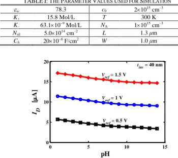
The method described in the last section was used to study the effect of various properties of ISFET pH sensor on the output current and on the two types of sensitivity defined in (10) and (11). The drain to source voltage is set to 0.2V. The other parameter values used for simulation are shown in Table I, in which, NA is the substrate doping, L is the gate
length, and W is the device width.
TABLEI:THE PARAMETER VALUES USED FOR SIMULATION
w 78.3 c0 21015 cm–3
K+ 15.8 Mol/L T 300 K
K– 63.1109 Mol/L N
A 11015 cm–3
Nsil 5.01014 cm–2 L 1.3 μm
Ch 20106 F/cm2 W 1.0 μm
0 5 10 15
0 5 10 15 20
Vref = 0.5 V
V
ref = 1 V
Vref = 1.5 V
pH
I D
[
A]
tins = 40 nm
Fig. 5. Drain current variation with pH value for an ISFET with gate insulator thickness tins = 40 nm at three different values of reference electrode voltage,
Vref = 0.5, 1, and 1.5 V .
Fig. 5 shows the variation of the drain current versus pH value for SiO2 gate-insulator of thickness tins = 40 nm at three
values of reference electrode voltage Vref, 0.5, 1, and 1.5 V.
The change in the drain current is seen to be relatively larger for small pH compared to high pH range. On the other hand, in Fig. 6, Vref is plotted against pH at three current levels of 10,
13, and 15 μA. The change in Vref is also larger at low pH
values. More quantitatively, in Fig. 7, the sensitivity S1 is
plotted versus pH for the same device at Vref, = 0.5, 1, and 1.5
V. Although the sensitivity generally decreases with increasing pH, however, it increases again for large pH, especially for small Vref. The use of large Vref satisfies higher
maximum sensitivity (attained at very low pH), but on the other hand, the use of small Vref gives better sensitivity at very
high pH. The same conclusion can be extracted from Fig. 8, in which, the other type of sensitivity S2 is plotted versus pH
for three level of drain currents, ID = 3, 10, and 17 μA.
Another design factor, which is the level of output drain current, can be viewed from Fig. 8. Small current levels are suitable for large pH solutions while large current levels are better for small pH solutions.
2 4 6 8 10 12 14
0.8 1 1.2 1.4 1.6
ID = 10 A
ID = 13 A
ID = 15 A
pH
V re
f
[
V
]
t
ins = 40 nm
Fig. 6. Reference electrode voltage versus pH for an ISFET with gate insulator thickness tins = 40 nm at three fixed current levels, ID = 10, 13, and
15 μA.
Fig. 7. ISFET sensitivity, S1 versus pH value at three values of Vref, 0.5, 1 and 1.5 V for a device of gate-insulator thickness tins = 40 nm. Sensitivity
deteriorates for large values of pH.
0 5 10 15 0
0.05 0.1 0.15 0.2 0.25 0.3 0.35
pH
S 1
=
dI
D
/dpH
[
A]
Vref = 0.7 V
tins =20 nm
tins =40 nm
tins =60 nm
tins =80 nm
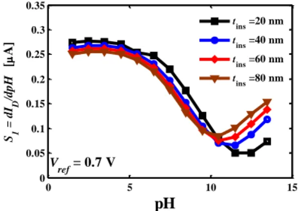
Fig. 9. ISFET sensitivity, S1 versus pH value at Vref = 0.7 V and for four gate-insulator thicknesses tins = 20, 40, 60, and 80 nm.
2 4 6 8 10 12 14
0 5 10 15 20 25
pH
S 2
=
V ref
/
(pH)
[mV]
I
D = 3 A
tins 20 nm
tins 40 nm
tins 60 nm
tins 80 nm
Fig. 10. ISFET sensitivity, S2 versus pH value at ID = 3 A and for four gate-insulator thicknesses tins = 20, 40, 60, and 80 nm.
Regarding the effect of gate-insulator thickness, Fig. 9 and 10 shows S1 at Vref = 0.7 V, and S2 at ID = 3 μA, versus pH for
four values of gate-insulator, tins = 20, 40, 60, 80 nm. It
should be noted that increasing tins has two conflicting effects,
the first is to lower the sensitivity at low pH (< 10), and the other is to increase the sensitivity at high pH (> 10). On the average, increasing tins will improve the sensitivity of the
device as a whole and guarantees a higher lower limit on the whole pH range. This will be on the expense of the decrease of output drain current.
V. CONCLUSION
A new methodology was proposed to extract the sensitivity of ISFET pH sensor. The methodology links charge and potential equations in the tested solution with a device simulation tool to account for MOSFET electrical properties. An initial guess for the potential at the insulator surface is assumed, then, simulation is performed to find the corresponding value of the external reference electrode voltage. The process is repeated until the calculated value is consistent with the real applied reference voltage. Various effects on ISFET sensitivity were investigated such as drain current level, reference voltage, pH range, and gate insulator thickness. It is found that the sensitivity is generally higher for low pH values. It is also found that working at low current levels and larger gate insulator thicknesses decreases the maximum sensitivity (at low pH), but on the other hand it gives the advantage of increasing the minimum sensitivity (at high pH).
ACKNOWLEDGMENT
The authors would like to thank Deanship of Scientific Research at Umm Al-Qura University for the financial support of this project under the grant number 43408011.
Tarek M. Abdolkader was born in Cairo, Egypt, in 1970. He received two B.S. degrees one in electrical engineering (electronics and communications) from the faculty of engineering, and the other in physics from the faculty of science, both from Ain-Shams University, Cairo, Egypt, in 1992 and 1996, respectively. He received M.S. and Ph.D. degrees in engineering physics from the faculty of Engineering, Ain-Shams University, Cairo, Egypt, in 2001 and 2005, respectively. He joined Faculty of Engineering, Benha University as an assistant professor in 2005 and worked as a post-doctoral research associate in the School of Electrical and Computer Engineering, Purdue University, USA between 2009 and 2010. He is currently in a leave with Electrical Engineering Department, Faculty of Engineering, Umm Al-Qura University, Holy Makka, Saudi Arabia. His research interests are modeling and simulation of Nano-electronic devices including MOSFETs, CNFETs, and ISFETs.
Abdulrahman Al-Ahdal received his BSc. degree in electrical engineering from KFUPM in 1989. After working for Saudi Electronics, he received his MSc degree in analogue and digital IC design in 1999 from Imperial College London. He spent few years in industry then joined the Electrical Engineering Department of Umm Al-Qura University as a lecturer in 2004. He gained his PhD at the Electrical Engineering Department of Imperial College London in 2012. His research interests include integrated circuits and systems for biomedical applications. He is currently an assistant professor at EE department, UQU, Makkah, Saudi Arabia. He is the vice dean of the Institute of Consultancy Research and Studies (ICRS), and head of the Engineering Research Center of the Research Deanship.
REFERENCES
[1] H. Nakazawa, R. Otake, M. Futagawa, F. Dasai, M. Ishida, and K. Sawada, “High-sensitivity charge-transfer-type ph sensor with quasi-signal removal structure,” IEEE Transactions on Electron Devices, vol. 61, pp. 136-140, 2014.
[2] U. Hashim, C. S. Weng, and L. W. Wen, “Fabrication of silicon nitride ion sensitive field-effect transistor (ISFET),” in Proc. Micro and 2013 IEEE Regional Symposium on Nanoelectronics (RSM), 2013, pp. 204-207.
[3] J. Dutta, “Modeling ion sensitive field effect transistors for biosensor applications,” International Journal of Advanced Research in Engineering and Technology (IJARET), vol. 1, pp. 38-57, June 2010. [4] Y. Hu and P. Georgiou, “A robust ISFET pH-measuring front-end for
chemical reaction monitoring,” IEEE Transactions on Biomedical Circuits and Systems, vol. 8, issue 2, pp. 1-11, 2014.
[5] A. V. Surmalyan, “Surface potential behavior in ISFET based bio-(chemical) sensors,” Armenian Journal of Physics, vol. 5, pp. 194-202, December 2012.
[6] Y. Liu, P. Georgiou, T. Prodromakis, T. G. Constandinou, and C. Toumazou, “An extended CMOS ISFET model incorporating the physical design geometry and the effects on performance and offset variation,” IEEE Transactions on Electron Devices, vol. 58, pp. 4414-4422, 2011.
[7] W. M. Siu and R. S. C. Cobbold, “Basic properties of the electrolyte-SiO2-Si system: Physical and theoretical aspects,”IEEE
Transactions on Electron Devices, vol. 26, pp. 1805-1815, 1979. [8] M. Grattarola, G. Massobrio, and S. Martinoia, “Modeling
H+-sensitive FETs with SPICE,” IEEE Transactions on Electron Devices, vol. 39, pp. 813-819, 1992.
[9] J. C. Dutta, “Ion sensitive field effect transistor for applications in bioelectronic sensors: A research review,” inProc. 2012 2nd National Conference on Computational Intelligence and Signal Processing (CISP), 2012, pp. 185-191.
[10] T. Ytterdal, Y. Cheng, and T. A. Fjeldly, Device Modeling for Analog and RF CMOS Circuit Design, John Wiley & Sons Ltd, 2003. [11] Silvaco. Technology Computer Aided Design (TCAD) software.
Ahmed Shaker received B.S. degree in electronics and communications from Electrical Engineering Department at Faculty of Engineering, Ain Shams University, Cairo, Egypt, in 1996. He received M.S. and Ph.D. from Engineering Physics Department, Faculty of Engineering, Ain Shams University, Cairo, Egypt, in 2003 and 2010, respectively. He is currently an assistant professor, Engineering Physics & Mathematics Department Faculty of Engineering, Ain Shams University, Cairo, Egypt. His fields of research are semiconductor physics, simulation and modeling of semiconductor power devices, nanoscale devices, and photovoltaics.